
Chapter 10
Combinational Logic Design
10.1 Introduction
Using the previous ideas, combinational logic circuits can be combined using either the first canonical form (sum of products) or the second canonical form (product of sums). However, in this text only the first canonical form will be considered, taking into account logic level 0 or 1 and propagation (time) delays in the cells.
Within a logic gate is an analog circuit consisting of transistors—either bipolar, using NPN and PNP bipolar junction transistors, or CMOS (complementary metal-oxide semiconductor), using N-channel MOS and P-channel MOS transistors. Logic gates in CMOS are of three different circuit architectures at the transistor level [Ref. 10.1]: static CMOS, dynamic CMOS, and pass transistor logic CMOS. Today, static CMOS logic is by far the dominant type used. It is built on a network of pMOS and nMOS transistors connected between the power supplies, as shown in Figure 10.1.
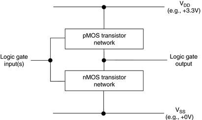
Figure 10.1 Static CMOS logic gate architecture
The input signals are connected to the gates of the transistors, and the output is taken from the common connection between the transistor networks. The transistors will act as switches, with the switch connections between the drain and source of the transistor. Switch control is via a gate voltage:
• An nMOS transistor will be switched ON when high voltage (logic 1) is applied to the transistor gate. Low voltage (logic 0) will turn the switch OFF.
• A pMOS transistor will be switched ON when low voltage (logic 0) is applied to the transistor gate. High voltage (logic 1) will turn the switch OFF.
In the transistor network, a series connection of nMOS transistors will produce an AND effect (i.e., both transistors must be switched ON for the combined effect to be ON). A parallel connection of nMOS transistors will produce an OR effect (i.e., any single transistor must be switched ON for the combined effect to be ON). For the pMOS transistor network, a series connection of nMOS transistors requires a parallel connection of pMOS transistors. A parallel connection of nMOS transistors requires a series connection of pMOS transistors.
The inverter is the most basic logic gate and, in static CMOS, consists of one nMOS and one pMOS transistor. The basic arrangement is shown in Figure 10.2.

Figure 10.2 Static CMOS inverter
The logic gate has both static (DC) and dynamic (time-related) characteristics. Both the voltage (at the different points in the circuit with reference to the common, 0V, node) and the currents (in particular the power supply current) must be considered.
The static characteristics of the inverter are shown in Figure 10.3; in this case, the static (DC) voltages are not time related. Two graphs are shown. The top graph plots the input voltage (VIN) against the output voltage (VOUT). This shows the operating regions (off, saturation, linear) that each transistor will go through during the input and output voltage changes. A logic 0 is a voltage level of VSS, and a logic 1 is a voltage level of VDD. The bottom graph plots the input voltage (VIN) against the current drawn from the power supply (IDD), showing that the current drawn from the power supply peaks during changes in the input and output voltages.

Figure 10.3 Static CMOS inverter—static characteristics
The dynamic characteristics of the inverter are shown in Figure 10.4. These show the operation of the inverter to changes of the inputs and outputs in time. The top graph shows the input test signal, which in this case is a step change for a 0-1-0 logic level change with an instantaneous change in logic value in time. The two voltage levels are VOL and VOH:
• VOL defines the maximum output voltage from the logic gate that would produce a logic 0 output.
• VOH defines the minimum output voltage from the logic gate that would produce a logic 1 output.
• The middle graph shows the output, which changes from a 1 to a 0 and a 0 to a 1 in a finite time. Two values for the propagation time delay are defined, tPHL and tPLH:
![]() tPHL defines a propagation time delay from a high level (1) to a low level (0) between the start of the input signal change and the 50% change in output.
tPHL defines a propagation time delay from a high level (1) to a low level (0) between the start of the input signal change and the 50% change in output.
![]() tPLH defines a propagation time delay from a low level (0) to a high level (1) between the start of the input signal change and the 50% change in output.
tPLH defines a propagation time delay from a low level (0) to a high level (1) between the start of the input signal change and the 50% change in output.
• The bottom graph shows the output, which changes from a 1 to a 0 and a 0 to a 1 in a finite time. Two values for the rise and fall times are defined, tFALL and tRISE:
![]() tFALL defines a fall time from a high level (1) to a low level (0) between the 90% and 10% levels between the high and low levels.
tFALL defines a fall time from a high level (1) to a low level (0) between the 90% and 10% levels between the high and low levels.
![]() tRISE defines a rise time from a low level (0) to a high level (1) between the 10% and 90% levels between the low and high levels.
tRISE defines a rise time from a low level (0) to a high level (1) between the 10% and 90% levels between the low and high levels.
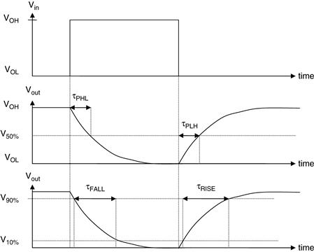
Figure 10.4 Static CMOS inverter—dynamic characteristics
Having considered the static CMOS inverter operation, the logical operation of more complex logic gates will be considered through the following four examples:
Example 10.1 Two-Input Multiplexer
Consider a circuit that has two data inputs (A and B) and one data output (Z). An additional control input, Select, is used to select which input appears at the output, such that:
This circuit is the multiplexer, and the circuit symbol is shown in Figure 10.5.
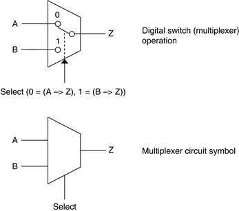
Figure 10.5 Two-input multiplexer
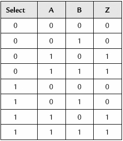
In general, the multiplexer can have as many data inputs as required, and the number of control signals required will reflect the number of data inputs. For the two-input multiplexer, the truth table has three inputs (for eight possible combinations) and the output as shown in Table 10.1. The Boolean expression can be created for this and a reduced form would be:
![]()
Table 10.1 Two-input multiplexer truth table
Although the multiplexer is normally available as a single logic gate in an ASIC or PLD reference library, the circuit could be created using discrete logic gates. The circuit schematic for this is shown in Figure 10.6. The inverse operation of the multiplexer (mux) is the demultiplexer (demux). This has one data input and multiple data outputs. The additional control inputs will select one output to be active and will pass the input data logic value to the particular output. As there are multiple outputs in the demultiplexer, the remaining outputs (those outputs which have not been selected) will output a logic “0” value.

Figure 10.6 Two-input multiplexer using discrete logic gates
Example 10.2 One-Bit Half-Adder
The half-adder is an important logic design created from basic logic gates, as shown in Figure 10.7. This is a design with two inputs (A and B) and two outputs (Sum and Carry-out, Cout). This cell adds the two binary input numbers to produce sum and carry-out terms.

Figure 10.7 One-bit half-adder cell
The truth table for this design is shown in Table 10.2.
Table 10.2 One-bit half-adder cell truth table

From viewing the truth table, the Sum output is only a logic 1 when either but not both inputs are logic 1:
![]()
This is actually the EX-OR function, so:
![]()
From viewing the Cout output in the truth table, the output is logic 1 only when both inputs are logic 1 (i.e., A AND B):
![]()
This can be drawn as a circuit schematic as shown in Figure 10.8.

Figure 10.8 One-bit half-adder circuit schematic
Example 10.3 One-Bit Full-Adder
The full-adder extends the concept of the half-adder by providing an additional carry-in (Cin) input, as shown in Figure 10.9. This is a design with three inputs (A, B, and Cin) and two outputs (Sum and Cout). This cell adds the three binary input numbers to produce sum and carry-out terms.

Figure 10.9 One-bit full-adder cell
The truth table for this design is shown in Table 10.3.
Table 10.3 One-bit full-adder cell truth table

From viewing the truth table, the Sum output is only a logic 1 when one or three (but not two) of the inputs is logic 1. The Boolean expression for this is (in reduced form):
![]()
From viewing the truth table, the Cout output is only a logic 1 when two or three of the inputs is logic 1. The Boolean expression for this is (in reduced form):
![]()
This can be drawn as a circuit schematic as shown in Figure 10.10.

Figure 10.10 One-bit full-adder circuit schematic
Any number of half- and full-adder cells can be connected together to form an n-bit addition. Figure 10.11 shows the connections for a four-bit binary adder. In this design, there is no Cin input. Inputs A and B are four bits wide, and bit 0 (A(0) and B(0)) are the LSBs.

Figure 10.11 Four-bit binary adder
Example 10.4 Partial Odd/Even Number Detector
Consider a circuit that receives a three-bit unsigned binary number (A, B, and C where A is the MSB and C is the LSB) and is to detect when the number is ODD or EVEN. The circuit will have two outputs (Odd and Even), as shown in Figure 10.12. The Odd output is a logic 1 when the input number (in decimal) is 1, 3, or 5 but not 7. The input 7 is to be considered a forbidden input in this circuit. The Even output is a logic 1 when the input number (in decimal) is 0, 2, 4, 6.
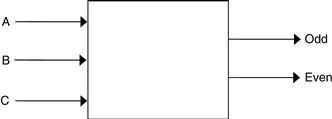
Figure 10.12 Number detector circuit block diagram
The truth table for this circuit is shown in Table 10.4.
Table 10.4 Three-input logic circuit truth table

A Boolean expression for each of the outputs can be created. However, because the Odd and Even outputs are inversions of each other (except in the forbidden state), a circuit can be created whereby the Boolean expression for one output is created and the second output is the inverse (NOT) of this output. Considering the Odd output (with three 1s, compared to four in the Even output, making it a smaller Boolean expression), then the Boolean expression for the Odd and Even outputs would be:


The circuit schematic for this design is shown in Figure 10.13.

Figure 10.13 Circuit schematic for odd/even number detector
A problem with this circuit is that when the odd number input 7 is applied, the circuit produces a logic 0 on Odd and a logic 1 on Even, which is incorrect. If this circuit is to be used, then the input 7 must be taken into account and the circuit redesigned, or the input 7 must never be applied by design.
If the input 7 is considered in the creation of the Boolean logic expression for the Odd output, then the logic for the Odd output simply becomes the value for the C input.
The basic arrangement is shown in Figure 10.14. Here, the CoolrunnerTM-II CPLD on the CPLD development board is configured with the digital logic circuit, and the digital I/O board is interfaced to external test and measurement equipment. The CPLD is configured using the pins identified in Table 10.5.

Figure 10.14 Odd/even number detector implementation using the CPLD development board
Table 10.5 Odd/even number detector CPLD pin assignment

Here, the five design I/Os are defined and are connected to the relevant CPLD pins to connect to Header A for the digital I/O board. In addition, the CPLD design must also incorporate two additional outputs to enable the tristate buffers used on the digital I/O board. Here, the enable (OE, output enable) pins on the tristate buffers must be tied to logic 0 to enable the buffers.
External circuitry is connected to the digital I/O board to provide the logic levels for inputs A, B, and C and to monitor the outputs Odd and Even where:
The CPLD is programmed from using an appropriate JTAG (Joint Test Action Group) programmer.
10.2 NAND and NOR Logic
Logical operations using AND, OR, and NOT logic gates can also be undertaken using either NAND or NOR logic gates. A Boolean expression using AND, OR, and NOT logic can be manipulated to produce NAND and NOR logic. For example, the Boolean expression:
![]()
can also be expressed as:
![]()
Figure 10.15 shows the two logic gate implementations for these Boolean expressions. Similarly, the Boolean expression:
![]()
can also be expressed as:
![]()
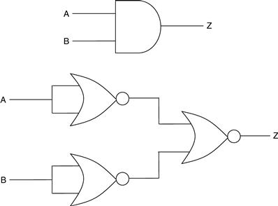
Figure 10.15 NOR implementation for the AND gate
Figure 10.16 shows the two logic gate implementations for these Boolean expressions.
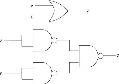
Figure 10.16 NAND implementation for the OR gate
If only NAND and NOR gates are available, any Boolean logic expression can be implemented through such manipulation.
10.3 Karnaugh Maps
The Karnaugh map (or K-map) provides a means to display logical operations on input signals as a map showing the output values for each of the input values. This allows groups of logic values to be looped together with suitably sized loops to minimize the resulting Boolean logic expression. The size of the Karnaugh map depends on the number of inputs to the combinational logic circuit. Karnaugh maps for two-, three-, and four-input circuits are shown in Figure 10.17:
• A two-input Karnaugh map contains four cells, one cell for each possible input combination (2n where n is the number of inputs). Here, the inputs are named A and B.
• A three-input Karnaugh map contains eight cells, one cell for each possible input combination (2n where n is the number of inputs). Here, the inputs are named A, B, and C.
• A four-input Karnaugh map contains sixteen cells, one cell for each possible input combination (2n where n is the number of inputs). Here, the inputs are named A, B, C, and D.

Figure 10.17 Two-, three-, and four-input Karnaugh maps
The Karnaugh map has a direct correspondence with the truth table for a Boolean logic expression. Each K-map cell is filled with the logic value of the output (0 or 1) for the corresponding input combination. In Figure 10.17, the cells are filled with (for reference purposes) the decimal number equivalent for the unsigned binary value of the input combination (A is the MSB of the binary input value). Note the values and locations of the values within the cells.
The Karnaugh maps for the two-input logic gates in Figure 9.4 are shown in Figure 10.18.
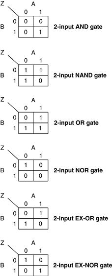
Figure 10.18 Truth table for two-input logic gates
The Karnaugh map can then be analyzed, and loops of output logic levels within the cells can be created. In the first canonical form, logic 1s are grouped together. In the second canonical form, logic 0s are grouped together. In this text, the first canonical form will be considered, so in the Karnaugh map, logic 1s are grouped together.
The larger the loop, the smaller the resulting Boolean logic expression (with fewer variables to be considered). The variables in the loop will be ANDed together, and each group will be ORed together.
For a two-input Karnaugh map, then:
• A group of one logic 1 will result in the ANDing of two variables.
• A group of two logic 1s will result in one variable.
• A group of four logic 1s will result in a constant logic 1.
For a three-input Karnaugh map, then:
• A group of one logic 1 will result in the ANDing of three variables.
• A group of two logic 1s will result in the ANDing of two variables.
• A group of four logic 1s will result in one variable.
• A group of eight logic 1s will result in a constant logic 1.
For a four-input Karnaugh map, then:
• A group of one logic 1 will result in the ANDing of four variables.
• A group of two logic 1s will result in the ANDing of three variables.
• A group of four logic 1s will result in the ANDing of two variables.
• A group of eight logic 1s will result in one variable.
• A group of sixteen logic 1s will result in a constant logic 1.
Consider the two-input AND gate: it has only one logic 1, so only a loop of 1 can be created, as shown in Figure 10.19. Where the input variable is a logic 1, the variable is used. When the input variable is a logic 0, the inverse (NOT) of the variable is used.

Figure 10.19 Two-input AND gate
Consider now the two-input OR gate: it has three logic 1s, two loops of two can be created, as shown in Figure 10.20. Where the input variable is a logic 1, the variable is used. When the input variable is a logic 0, the inverse (NOT) of the variable is used.

Figure 10.20 Two-input OR gate
When a group of two is created, one of the variables can be a logic 0 or a logic 1 and so can be dropped from the resulting Boolean logic expression. The vertical group of two retains the variable A but drops the variable B. The horizontal group of two retains the variable B but drops the variable A.
The grouping of logic 1s follows the following rules:
1. Loops of 2n adjacent cells can be made where n is an integer number starting at 0.
2. All cells containing a 1 (first canonical form; or 0 in the second canonical form) must be covered.
3. Loops can overlap provided they contain at least one unlooped cell.
4. Loops must be square or rectangular (diagonal or L-shaped loops are not permitted).
5. Any loop that has all of its cells included in other loops is redundant.
6. The edges of a map are considered to be adjacent—a loop can leave the side of the Karnaugh map and re-enter at the other side, or leave from the top of the Karnaugh map and return at the bottom, as shown in Figure 10.21.

Figure 10.21 Adjacent cells in a Karnaugh map
One potential problem with combinational logic arises from hazards. Here, because of the finite time for a signal change to propagate through the combinational logic (due to any logic gate delays and interconnect delays), there is potential for erroneous output during the time that the change occurs. This results from different time delays in different paths within the combinational logic. Although the final output would be correct, an erroneous output (i.e., wrong logic level) can occur during the change, which would cause problems if detected and used.
If the digital circuit or system can be designed so that the output from the combinational logic with a hazard is only used after it is guaranteed correct, then the hazard, although not eliminated, will not cause a problem in the design.
A way to eliminate hazards using the Karnaugh map is to ensure that all loops are joined together. Although this will introduce a redundant term (see Figure 10.22), the hazard will be removed. However, this is at the expense of using additional logic and introducing potential problems with testing the design [Ref. 10.2].

Figure 10.22 Eliminating hazards
Two important points to note with logic gates are:
1. No input to a logic gate may be left unconnected. If an input to a logic gate is not required, then it must be tied to logic level (0 or 1). This is usually achieved by connecting a high-resistance value resistor (typically 10 to 100 kΩ) between the unused input and one of the power supply connections (VDD for logic 1, VSS or GND for logic 0). In some ICs, specific inputs might be designed for use only under specific circumstances and with a pull-up (to logic 1) or pull-down (to logic 0) component integrated into the IC circuitry. Such integrated pull-up or pull-down components alleviate the need for the designer to place resistors on the PCB and so reduce the PCB design requirements.
2. Where a logic gate only produces a logic 0 or 1 output, then no two or more logic gate outputs are to be connected unless the implementation technology (circuitry within the logic gate) allows it. Certain logic gate outputs can be put into a high-impedance state, which stops the output from producing a logic output and instead turns the output into a high-impedance electrical load. Circuits with a high-impedance output are used where multiple devices are to be connected to a common set of signals (a bus) such as a microprocessor data bus.
Whereas the previous logic gates considered in the design of digital circuits using Boolean logic expressions, truth tables, and Karnaugh maps provided only a logic 0 or 1 output, in many computer architectures, multiple devices share a common set of signals—control signals, address lines, and data lines. In a computer architecture where multiple devices share a common set of data lines, these devices can either receive or provide logic levels when the device is enabled (and all other devices are disabled). However, multiple devices could, when enabled, provide logic levels at the same time; these logic levels typically conflict with the logic levels provided by the other devices. To prevent this, rather than producing a logic level when disabled, a device would be put in a high-impedance state (denoted by the character Z). The tristate buffer, when enabled, passes the logic input level to the output; when disabled, it blocks the input, and the output is seen by the circuit that it is connected to as a high-impedance electrical load. This operation is shown in Figure 10.23, in which the enable signal may be active high (top, 1 to enable the buffer) or active low (bottom, 0 to enable the buffer).
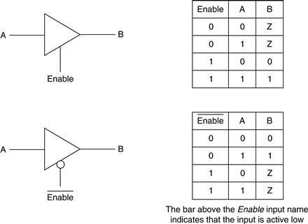
Figure 10.23 Tristate buffer symbol
10.4 Don’t Care Conditions
In some situations, certain combinations of input might not occur, so the designer could consider that these conditions are not important. They are referred to as Don’t care conditions. As such, the output in these conditions could be either a logic 0 or a logic 1, so the designer is free to choose the output value that results in the simpler output logic (i.e., using fewer logic gates).
REFERENCES
[10.1] Kang S, Leblebici Y. CMOS Digital Integrated Circuits Analysis and Design Singapore: McGraw-Hill International Editions; 1996; ISBN 0-07-114423-4.
[10.2] Grout IA. Integrated Circuit Test Engineering Modern Techniques Springer 2006; ISBN 1-84628-023-0.