
Chapter 9
Binary Data Manipulation
9.1 Introduction
A digital circuit or system utilizes and manipulates binary data to perform a required operation. Essentially, groups of bits of data are converted from one value to another at a particular point in time. Software-programmed processors typically manipulate groups of 8, 16, 32, 64, or 128 bits of data, although a custom design could manipulate as many bits as required.
Binary data is manipulated using the following:
• Boolean logic provides a means to display the operations on input signals and produce a result in mathematical terms using AND, NAND, OR, NOR, EXOR, EX-NOR, and NOT logical operations.
• Truth tables provide a means to display the operations on input signals and produce a result in table format.
• Karnaugh maps provide a means to display the operations on input signals and produce a result on a K-map, which allows logic values to be grouped together with loops.
• Circuit schematics provide a graphical representation of the Boolean logic expression using logic gate symbols for the logical operations and the connections between the terminals.
Boolean logic, truth tables, Karnaugh maps, and circuit schematics are used in the design and analysis of digital circuits and systems, and the designer must move between these different representations of circuit and system operation many times during the design process. However, these tools are really only suited for design by hand (as it were) for small circuits; for more complex circuits and systems, hardware description languages (HDL) are more commonly used. Understanding Boolean logic, truth tables, and Karnaugh maps, however, will provide the designer with the necessary skills to design, develop, and debug circuit and system designs of any size and complexity.
9.2 Logical Operations
A digital circuit or system will consist of a number of operations on logic values. The basic logical operators are the:
Considering two inputs (here called A and B) to a logical operator, the AND, OR, and EX-OR operators provide different results:
• The AND operator provides an output when both A and B are at the required values.
• The NAND operator provides an output that is the inverse of the AND operator.
• The OR operator provides an output when either or both A and B are at the required values.
• The NOR operator provides an output that is the inverse of the OR operator
• The EX-OR operator provides an output when either but not both A and B are at the required values.
• The EX-NOR (or equivalence) operator provides an output that is the inverse of the EX-OR operator.
The NOT operator provides an output that is the logical inverse of the input.
In addition, the BUFFER will provide an output that is the same logic level value as the input. The BUFFER is essentially two NOT gates in series.
These logical operators function in electronic hardware as logic gates. Two inputs (A and B) to the logic gate were considered above, but more inputs are possible to certain logic gates.
9.3 Boolean Algebra
Boolean algebra (developed by George Boole and Augustus De Morgan) forms the basic set of rules that regulate the relationship between true-false statements in logic. Applied to digital logic circuits and systems, the true-false statements regulate the relationship between the logic levels (logic 0 and 1) in digital logic circuits and systems. The relationships are based on variables and constants:
• The identifier for the AND logical operator is . (the dot).
• The identifier for the OR logical operator is + (the mathematical addition symbol).
• The identifier for the NOT logical operator is ¯¯ (a bar across the expression).
• The identifier for the EX-OR logical operator is ⊕ (an encircled addition symbol).
Figure 9.1 shows the Boolean logic expression for each of these operators.

Figure 9.1 Boolean expressions for the basic logic operators
Each of the operators can be combined to create more complex Boolean logic expressions. For example, if a circuit has four inputs (A, B, C, and D) and one output (Z), then if Z is a logic 1 when (A and B) is a logic 1 or when (C and D) is a logic 1, the Boolean expression is:
![]()
Here, parentheses are used to group the ANDed variables and to indicate precedence among various operations—similar to their use in other mathematical expressions. The AND logical operator has a higher precedence than the OR logical operator and so would be naturally grouped together in this way.
A Boolean expression written using Boolean algebra can be manipulated according to a number of theorems to modify it into a form that uses the right logic operators (and therefore the right type of logic gate) and to minimize the number of logic gates. The theorems of Boolean algebra fall into three main categories:
Table 9.1 summarizes the logical operations on constants. Each constant value can be either a logic 0 or 1. The result is either a logic 0 or 1 according to the logic operator. A bar above the constant indicates a logical inversion of the constant.
Table 9.1 Logical operations on constants

Table 9.2 summarizes the logical operations on one variable (A). The operation is performed on the variable alone or on a variable and a constant value. Each variable and constant value can be either a logic 0 or 1. The result is either a logic 0 or 1 according to the logic operator.
Table 9.2 Logical operations on one variable

A bar above the variable indicates a logical inversion of the variable. A double bar indicates a logical inversion followed by another logical inversion. Using the circuit symbol for the NOT gate (the symbol is a triangle with a circle at the end—see Figure 9.4), this effect is shown in Figure 9.2. Logically, a double inversion of a signal has no logical effect.

Figure 9.2 Inverting a variable
In practice, the logic gates used to create each of the inversions would create a propagation delay of the value of the variable as it passes through each logic gate. However, a double inversion produces a logic buffer, as shown in Figure 9.3.

Figure 9.3 Logic buffer schematic symbol
The buffer can be used to allow for a signal to drive a large electrical load.
Table 9.3 summarizes the logical operations on two or more variables. Here, two (A and B) or three variables (A, B, and C) are considered. Each variable value can be either a logic 0 or 1. The result is either a logic 0 or 1 according to the logic operator.
Table 9.3 Logical operations on two or three variables
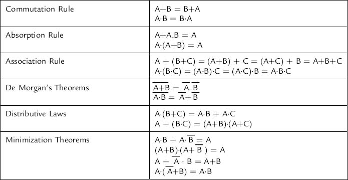
The commutation rule states that there is no significance in the order of placement of the variables in the expression. The absorption rule is useful for simplifying Boolean expressions, and the association rule allows variables to be grouped together in any order. De Morgan’s theorems are widely used in digital logic design as they allow for AND logical operators to be related to NOR logical operators and OR logical operators to be related to NAND logical operators, which allows Boolean expressions to take different forms and thereby be implemented using different logic gates. The distributive laws allow a process similar to factorization in arithmetic, and the minimization theorems allow Boolean expressions to be reduced to a simpler form.
9.4 Combinational Logic Gates
Each logic gate that implements the logical operators is represented by a circuit symbol. The commonly used symbols are shown in Figure 9.4. Here, for each logic gate, the inputs are A or A and B, and the output is Z.

Figure 9.4 Logical operator circuit symbols
An alternative set of logic symbols, IEEE/ANSI standard 91-1984 (Graphics Symbols for Logic Functions [Refs. 9.1, 9.2]), is shown in Figure 9.5.

Figure 9.5 Sample IEEE/ANSI standard logic symbols
Figures 9.4 and 9.5 use only two-input logic gates for the AND, NAND, OR, and NOR gates, but it is common to use these logic gates with more than two inputs. For example, up to six inputs are available for use in many PLD and ASIC design libraries.
9.5 Truth Tables
The truth table displays the logical operations on input signals in a table format. Every Boolean expression can be viewed as a truth table. The truth table identifies all possible input combinations and the output for each. It is common to create the table so that the input combinations produce an unsigned binary up-count.
The truth table for the AND gate is shown in Table 9.4. Here, the output Z is a logic 1 only when both inputs A and B are logic 1.
Table 9.4 AND gate truth table
| A | B | Z |
| 0 | 0 | 0 |
| 0 | 1 | 0 |
| 1 | 0 | 0 |
| 1 | 1 | 1 |
The truth table for the NAND gate is shown in Table 9.5. Here, the output Z is a logic 0 only when both inputs A and B are logic 1. This is the logical inverse of the AND gate.
Table 9.5 NAND gate truth table
| A | B | Z |
| 0 | 0 | 1 |
| 0 | 1 | 1 |
| 1 | 0 | 1 |
| 1 | 1 | 0 |
The truth table for the OR gate is shown in Table 9.6. Here, the output Z is a logic 1 when either or both inputs A and B are logic 1.
Table 9.6 OR gate truth table
| A | B | Z |
| 0 | 0 | 0 |
| 0 | 1 | 1 |
| 1 | 0 | 1 |
| 1 | 1 | 1 |
The truth table for the NOR gate is shown in Table 9.7. Here, the output Z is a logic 0 when either or both inputs A and B are logic 1. This is the logical inverse of the OR gate.
Table 9.7 NOR gate truth table
| A | B | Z |
| 0 | 0 | 1 |
| 0 | 1 | 0 |
| 1 | 0 | 0 |
| 1 | 1 | 0 |
The truth table for the EX-OR gate is shown in Table 9.8. Here, the output Z is a logic 1 when either but not both inputs A and B are logic 1.
Table 9.8 EX-OR gate truth table
| A | B | Z |
| 0 | 0 | 0 |
| 0 | 1 | 1 |
| 1 | 0 | 1 |
| 1 | 1 | 0 |
The truth table for the EX-NOR gate is shown in Table 9.9. Here, the output Z is a logic 0 when either but not both inputs A and B are logic 1. This is the logical inverse of the EX-OR gate.
Table 9.9 EX-NOR gate truth table
| A | B | Z |
| 0 | 0 | 1 |
| 0 | 1 | 0 |
| 1 | 0 | 0 |
| 1 | 1 | 1 |
The truth table for the NOT gate (inverter) is shown in Table 9.10. This gate has one input only. The output Z is the logical inverse of the input A.
Table 9.10 NOT gate truth table
| A | Z |
| 0 | 1 |
| 1 | 0 |
The truth table for the BUFFER is shown in Table 9.11. This gate has one input only. The output Z is the same logical value as that of the input A.
Table 9.11 BUFFER truth table
| A | Z |
| 0 | 0 |
| 1 | 1 |
Another way to describe a digital circuit or system is by using a suitable HDL such as VHDL [Refs. 9.3, 9.4]. This describes the operation of the circuit or system at different levels of design abstraction. An example VHDL description for each of the basic logic gates using the built-in logical operators in VHDL is shown in Figure 9.6. It is sufficient at this point to note that HDLs exist and for VHDL the basic structure of a VHDL text based description is of the form shown in Figure 9.6.


Figure 9.6 VHDL code examples for the logic gates in Figure 9.4
The EX-OR gate has the Boolean expression:
![]()
From the truth table for the EX-OR gate, then, a Boolean expression in the first canonical form (the first canonical from is a set of minterms that are AND logical operators on the variables within the expression with the output of the AND logical operators being logically ORed together) can be written as:
![]()
Therefore, the EX-OR gate can be made from AND, OR, and NOT gates as shown in Figure 9.7.

Figure 9.7 EX-OR gate using discrete logic gates
The truth table can be created to identify the input-output relationship for any logic circuit that consists of combinational logic gates and that can be expressed by Boolean logic. It is therefore possible to move between Boolean logic expressions and truth tables. Consider a three-input logic circuit (A, B, and C) with one output (Z), as shown in the truth table in Table 9.12. The inputs are written as a binary count starting at 010 and incrementing to 710. The output Z is only a logic 1 when inputs A, B, and C are logic 1. This can be written as a Boolean expression:
![]()
Table 9.12 Three-input logic circuit truth table: Z = A.B.C

Here, where the output Z is a logic 1, the values of inputs A, B, and C are ANDed together. Where a variable is a logic 1, then the variable is used. When the variable is a logic 0, then the inverse (NOT) of the variable is used.
Consider now another three-input logic circuit (inputs A, B, and C) with one output (Z), shown in Table 9.13. The inputs are written as a binary count starting at 010 and incrementing up to 710. The output Z is only a logic 1 when inputs A, B, and C are logic 0. This can be written as a Boolean expression:
![]()
Table 9.13 Three-input logic circuit truth table: Z = NOT (A + B + C)

Here, where the output Z is a logic 1, the values of inputs A, B, and C are ANDed together. Where a variable is a logic 1, then the variable is used. When the variable is a logic 0, then the inverse (NOT) of the variable is used. The expression identified for the truth table in Table 9.13 can be modified using rules and laws identified in Table 9.3:
The original expression was manipulated by first double-inverting the expression (which logically makes no change), then breaking one of the inversions (the inversion closest in space to the variables) and changing the AND operator to an OR operator (the second De Morgan theorem). This leaves a NOR expression with double-inverted variables. The double-inversion on each input is then dropped.
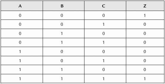
Now, combining the operations in Table 9.12 and Table 9.13 produces a more complex operation as shown in Table 9.14.
Table 9.14 Three-input logic circuit truth table: complex logic gate
The Boolean expression for this is:
![]()
Each of the ANDed expressions is ORed together. Parentheses group each expression to aid readability of the expression. In this form of expression, the first canonical form, a set of minterms (minimum terms) that are AND logical operators are created (one for each line of the truth table where the output is a logic 1). The outputs for each of the AND logical operators are ORed together. This is also referred to as a sum of products. A circuit schematic for this circuit is shown in Figure 9.8.

Figure 9.8 Circuit schematic for Boolean expression in Table 9.14
The second canonical form is an alternative to the first canonical form. In the second, a set of maxterms that are OR logical operators on the variables within the expression are created (one for each line of the truth table where the output is a logic 0). The outputs for each of the OR logical operators are ANDed together. This is also referred to as a product of sums.
Using these approaches, any Boolean logic expression can be described, analyzed, and possibly minimized.
REFERENCES
[9.1] The Institute of Electrical and Electronics Engineers, IEEE Standard, 91-1984, Graphics Symbols for Logic Functions, IEEE, USA.
[9.2] Overview of IEEE Standard 91-1984. Explanation of Logic Symbols USA: Texas Instruments; 1996.
[9.3] The Institute of Electrical and Electronics Engineers, IEEE Standard, 1076-2002, IEEE Standard VHDL Language Reference Manual, IEEE, USA.
[9.4] Zwolinski M. Digital System Design with VHDL England: Pearson Education Limited; 2000; ISBN 0-201-36063-2.