
Chapter 12
Memory
12.1 Introduction
Memory is used to store, provide access to, and allow modification of data and program code for use within a processor-based electronic circuit or system. The two basic types of memory are ROM (read-only memory, and RAM (random access memory). Memory can be considered for use for one of the following three data or program storage purposes:
1. Permanent storage for values that are normally only read within the application and can be changed (if at all) only by removing the memory from the application and reprogramming or replacing it.
2. Semi-permanent storage for values that can be read only within the application (as with permanent storage). However, stored values can be modified by reprogramming while the memory remains in the circuit.
3. Temporary storage for values needed only for temporary use and requiring fast access or modification (such as data and program code within a computer system that can be removed when no longer needed).
These memories are typically used within a computer architecture of the form shown in Figure 12.1. Here, the ROM and RAM are connected to the other computer functional blocks:
• ALU, arithmetic and logic unit;
• I/O, input/output to external circuitry; and
• controller to provide the necessary timing for the circuitry.
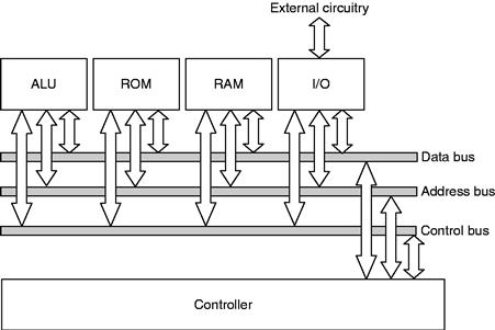
Figure 12.1 Basic computer architecture
Each of the functional blocks is connected to a common set of data, address, and control lines required to access and manipulate the digital data at specific points in time. Also needed is a power supply for each circuit to implement the functional blocks within the computer.
The key drivers for memory development are driven by the end-user, who is constantly demanding more functionality at a lower cost. Hence, the key drivers for memory development are:
1. increased capacity—the amount of data that can be stored within a single memory circuit;
2. increased operating speed—to reduce time to write data to and read data from the memory; and
Memory bandwidth, the amount of information that can be transferred to and from memory per unit time, is an increasingly important aspect to memory design and choice for use. This is driven by the increase in processor performance and demanding applications such as multimedia and communications.
12.2 Random Access Memory
RAM (also referred to as read-write memory, RWM) is considered volatile storage because its contents are lost when the power is removed. There are two main types of RAM, static RAM (SRAM) and dynamic RAM (DRAM). In addition, ferromagnetic RAM (FRAM) is also available.
A view of SRAM connections where the SRAM is provided in a dual in-line package (DIP) is shown in Figure 12.2. Here, the SRAM consists of the following connections:
• Address lines define the memory location to be selected for reading or writing.
• Input/output data lines define the data to write to or read from memory.
• Write enable (WE) is a control input that selects between the memory read and write operations (usually active low).
• Output enable (OE) is a control input that enables the output buffer for reading data from the memory (usually active low).
• Chip select (CS) selects the memory (usually active low).
• Power supply provides the necessary power to operate the circuit.

Figure 12.2 SRAM in a DIL package
Where the SRAM is provided as a discrete packaged device, a suitable power supply (VDD/VSS) along with power supply decoupling (capacitors) on the PCB will be needed. Increasingly, SRAMs are provided as macro cells within ICs (such as in the Xilinx® Spartan™-3 FPGA), in which the power supply has already been routed and the SRAM is ready for use.
In some RAM designs, the two write enable (WE) and output enable (OE) control signals identified above are combined into a single read/write (R/W) control signal. This reduces the pin count by one and the logic level of the R/W input will determine if the RAM is written to, or read from.
12.3 Read-Only Memory
ROM is used for holding program code that must be retained when the memory power is removed, so it is considered nonvolatile storage. The code can take one of three forms:
1. Fixed when the memory is fabricated—mask-programmable ROM.
2. Electrically programmed once—PROM, programmable ROM.
3. Electrically programmed multiple times—EPROM (electrically programmable ROM) erased using ultraviolet (UV) light; EEPROM or E2PROM (electrically erasable PROM); and Flash (also electrically erased).
PROM is sometimes considered in the same category of circuit as programmable logic, although in this text, PROM is discussed only in the memory category.
RAM is used for holding data and program code that must be accessed quickly and modified during normal operation. RAM differs from read-only memory (ROM) in that it can be both read from and written to in the normal circuit application. However, flash memory is also referred to as nonvolatile RAM (NVRAM).
A basic ROM design in which ROM is provided in a dual in-line package is shown in Figure 12.3. Here, the ROM consists of the following connections:
• Address lines define the memory location to be selected for reading or writing.
• Output data lines access the data from memory.
• Output enable (OE) is a control input that enables the output buffer for reading data from the memory (usually active low).
• Chip select (CS) selects the memory (usually active low).
• Power supply provides the necessary power to operate the circuit.
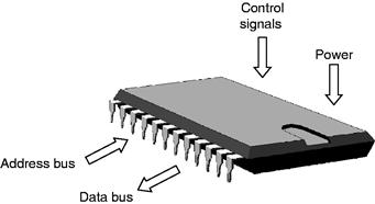
Figure 12.3 Basic ROM in a DIL package
In this view, the data bus is considered to be unidirectional (i.e., output only). Where the ROM may be electrically programmed, then the data and control line arrangement will be more complex.