
Chapter 28
Complex Programmable Logic Devices (CPLDs)
Complex programmable logic devices are exactly what they claim to be: logic devices that are complex and programmable. There are two main engineering features to understand about CPLDs that separate them from their cousins, FPGAs. One feature is the internal architecture of the device and how this architecture implements various logic functions. The second feature is the semiconductor technology that allows the devices to be programmed and allows various structures in the device to be connected.
28.1 CPLD Architectures
Essentially, CPLDs are designed to appear just like a large number of PALs in a single chip, connected to each other through a crosspoint switch. This architecture made them familiar to their target market—PC board designers who were already designing PALs in their boards. Many CPLDs were used to simply combine multiple PALs in order to save real estate on a PC board. CPLDs use the same development tools and programmers as PALs, and are based on the same technologies as PALs, but they can handle much more complex logic and more of it.
The diagram in Figure 28.1 shows the internal architecture of a typical CPLD. Although each manufacturer has a different variation, in general they are all similar in that they consist of function blocks, input/output blocks, and an interconnect matrix.

Figure 28.1 CPLD architecture
(courtesy of Altera Corporation)
28.2 Function Blocks
A typical function block is shown in Figure 28.3. Notice the similarity to the PAL architecture with its wide AND plane and fixed number of OR gates. The AND plane is shown by the crossing wires on the left. The AND plane can accept inputs from the I/O blocks, other function blocks, or feedback from the same function block. Programming elements at each intersection in the AND plane allow perpendicular traces to be connected or left open, creating “product terms,” which are multiple signals ANDed together, just like in a PAL. The product terms are then ORed together and sent straight out of the block, or through a clocked flip-flop. The Boolean equation in Figure 28.2 has four product terms.

Figure 28.2 Boolean equation with four product terms
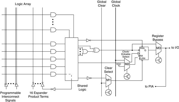
Figure 28.3 CPLD function block
(courtesy of Altera Corporation)
There are also multiplexers in the diagram, shown as boxes labeled M1, M2, and M3. Each mux has an FET transistor beneath it, representing a programmable element attached to the select line. In other words, the mux can be programmed to output one of the inputs. M1 is the “Clear Select” because it selects the signal that is used to clear the flip-flop. The M2 mux is labeled “Clock/Enable Select” because its two outputs are programmed to control the clock and clock enable input to the flip-flop. The M3 mux is labeled “Register Bypass” because it is programmed to determine whether the output of the functional block is a registered signal (i.e., is the output of a flip-flop) or a combinatorial signal (i.e., is the output of combinatorial logic).
Many CPLDs include additional, specialized logic. This particular block includes an exclusive OR, which can be effectively bypassed by programming one input to always be a 0. An XOR can be a nice gate to have because it is otherwise difficult to implement this function in a PAL. Exclusive ORs are used to easily generate parity in a bus for simple error detection.
Though not explicitly shown in Figure 28.3, each functional block would have many OR gates, logic gates, muxes, and flip-flops. Usually, the function blocks are designed to be similar to existing PAL architectures, such as the 22V10, so that the designer can use familiar tools to design them. They may even be able to fit older PAL designs into the CPLD without changing the design.
28.3 I/O Blocks
Figure 28.4 shows a typical I/O block of a CPLD. The I/O block is used to drive signals to the pins of the CPLD device at the appropriate voltage levels (e.g., TTL, CMOS, ECL, PECL, or LVDS). The I/O block typically allows each I/O pin to be individually configured for input, output, or bidirectional operation. The I/O pins have a tri-state output buffer that can be controlled by global output enable signals or directly connected to ground or VCC. Each output pin can also be configured to be open drain. In addition, outputs can often be programmed to drive different voltage levels, enabling the CPLD to be interfaced to many different devices.
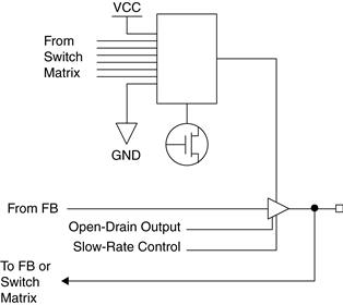
Figure 28.4 CPLD input/output block
(courtesy of Altera Corporation)
One particularly useful feature in high speed CPLDs is the ability to control the rise and fall rates of the output drivers by using a slew rate control. Designers can configure the output buffers for fast rise and fall times or for slow transition times. An advantage of the fast speed of these devices is less delay through the logic. A disadvantage of faster transition is times that they can cause overshoot and undershoot, which can potentially damage the device that the CPLD is driving. Also, fast transitions introduce noise, which can create problems. By programming the slew rate of the output buffer to a relatively slow transition, you can preserve the small logic delays of the device while avoiding undershoot, overshoot, and noise problems.
The input signal from the I/O block goes into the switch matrix in order to be routed to the appropriate functional block. In some architectures, particular inputs have direct paths to particular functional blocks in order to lower the delay on the input, reducing the signal setup time. In most architectures, specific pins of the device connect to specific I/O blocks that can drive global signals like reset and clock. This means that only certain pins of the device can be used to drive these global signals. This is particularly important for clock signals, as described in the next section.
28.4 Clock Drivers
Synchronous design is the only accepted design methodology that will ensure that a CPLD-based design is reliable over its lifetime. In order to design synchronous CPLDs, the clock signal must arrive at each flip-flop in the design at about the same time and with very little delay from the input pin. In order to accomplish this, special I/O blocks have clock drivers that use very fast input buffers and which drive the input clock signal onto an internal clock tree. The clock tree is so named because it resembles a tree, with each branch driving the clock input of a fixed number of flip-flops. The clock driver is designed to drive the entire tree very quickly. The trees are designed to minimize the skew between clock signals arriving at different flip-flops throughout the device. Each branch of the tree is of approximately equal length, or if not, internal buffers are used to balance the skew along the different branches. It is important that clock signals are only driven through the clock input pins that connect to these special drivers.
In large devices, there may be several clock input pins connected to different clock drivers. This feature helps in designs that use multiple clocks. You need to have at least as many clock drivers in the CPLD as you need clocks in your design. Also, the different clocks must be considered to be asynchronous with respect to each other, because the CPLD vendor does not typically guarantee skew between multiple clocks. Signals clocked by one clock will need to be synchronized with the other clock before use by any logic clocked by the second clock.
28.5 Interconnect
The CPLD interconnect is a very large programmable switch matrix that allows signals from all parts of the device to go to all other parts of the device. Figure 28.5 shows the architecture of the switch matrix. The switch matrix takes the outputs of the functional blocks and is programmed to send those outputs to functional blocks. This way, the designer can route any output signal to any destination.
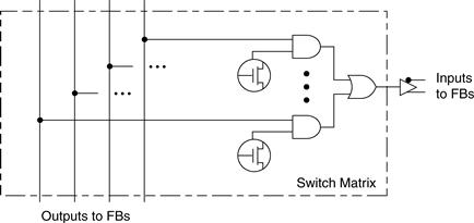
Figure 28.5 CPLD switch matrix
(courtesy of Altera Corporation)
One advantage of the CPLD switch matrix routing scheme is that delays through the chip are deterministic. Designers can determine the delay for any signal by computing the delay through functional blocks, I/O blocks, and the switch matrix. All of these delays are fixed, and delays due to routing the signal along the metal traces are negligible. If the logic for a particular function is complex, it may require several functional blocks, and thus several passes through the switch matrix, to implement.
Computing Parity without Exclusive OR
The Boolean expression for generating even parity for a bus is shown in the following equation:
parity = a0 ^ a1 ^ a2 ^ a3 ^ a4 ^ a5 ^ a6 ^ a7
If we implement this equation using AND and OR logic, the result is:
parity = a0 & !a1 & !a2 & !a3 & !a4 & !a5 & !a6 & !a7
| !a0 & a1 & !a2 & !a3 & !a4 & !a5 & !a6 & !a7
| a0 & a1 & a2 & !a3 & !a4 & !a5 & !a6 & !a7
| !a0 & !a1 & a2 & !a3 & !a4 & !a5 & !a6 & !a7
| a0 & !a1 & a2 & a3 & !a4 & !a5 & !a6 & !a7
| !a0 & a1 & a2 & a3 & !a4 & !a5 & !a6 & !a7
| a0 & a1 & !a2 & a3 & !a4 & !a5 & !a6 & !a7
| !a0 & !a1 & !a2 & a3 & !a4 & !a5 & !a6 & !a7
| a0 & !a1 & !a2 & a3 & a4 & !a5 & !a6 & !a7
| !a0 & a1 & !a2 & a3 & a4 & !a5 & !a6 & !a7
| a0 & a1 & a2 & a3 & a4 & !a5 & !a6 & !a7
| !a0 & !a1 & a2 & a3 & a4 & !a5 & !a6 & !a7
| a0 & !a1 & a2 & !a3 & a4 & !a5 & !a6 & !a7
| !a0 & a1 & a2 & !a3 & a4 & !a5 & !a6 & !a7
| a0 & a1 & !a2 & !a3 & a4 & !a5 & !a6 & !a7
| !a0 & !a1 & !a2 & !a3 & a4 & !a5 & !a6 & !a7
| a0 & !a1 & !a2 & !a3 & a4 & a5 & !a6 & !a7
| !a0 & a1 & !a2 & !a3 & a4 & a5 & !a6 & !a7
| a0 & a1 & a2 & !a3 & a4 & a5 & !a6 & !a7
| !a0 & !a1 & a2 & !a3 & a4 & a5 & !a6 & !a7
| a0 & !a1 & a2 & a3 & a4 & a5 & !a6 & !a7
| !a0 & a1 & a2 & a3 & a4 & a5 & !a6 & !a7
| a0 & a1 & !a2 & a3 & a4 & a5 & !a6 & !a7
| !a0 & !a1 & !a2 & a3 & a4 & a5 & !a6 & !a7
| a0 & !a1 & !a2 & a3 & !a4 & a5 & !a6 & !a7
| !a0 & a1 & !a2 & a3 & !a4 & a5 & !a6 & !a7
| a0 & a1 & a2 & a3 & !a4 & a5 & !a6 & !a7
| !a0 & !a1 & a2 & a3 & !a4 & a5 & !a6 & !a7
| a0 & !a1 & a2 & !a3 & !a4 & a5 & !a6 & !a7
| !a0 & a1 & a2 & !a3 & !a4 & a5 & !a6 & !a7
| a0 & a1 & !a2 & !a3 & !a4 & a5 & !a6 & !a7
| !a0 & !a1 & !a2 & !a3 & !a4 & a5 & !a6 & !a7
| a0 & !a1 & !a2 & !a3 & !a4 & a5 & a6 & !a7
| !a0 & a1 & !a2 & !a3 & !a4 & a5 & a6 & !a7
| a0 & a1 & a2 & !a3 & !a4 & a5 & a6 & !a7
| !a0 & !a1 & a2 & !a3 & !a4 & a5 & a6 & !a7
| a0 & !a1 & a2 & a3 & !a4 & a5 & a6 & !a7
| !a0 & a1 & a2 & a3 & !a4 & a5 & a6 & !a7
| a0 & a1 & !a2 & a3 & !a4 & a5 & a6 & !a7
| !a0 & !a1 & !a2 & a3 & !a4 & a5 & a6 & !a7
| a0 & !a1 & !a2 & a3 & a4 & a5 & a6 & !a7
| !a0 & a1 & !a2 & a3 & a4 & a5 & a6 & !a7
| a0 & a1 & a2 & a3 & a4 & a5 & a6 & !a7
| !a0 & !a1 & a2 & a3 & a4 & a5 & a6 & !a7
| a0 & !a1 & a2 & !a3 & a4 & a5 & a6 & !a7
| !a0 & a1 & a2 & !a3 & a4 & a5 & a6 & !a7
| a0 & a1 & !a2 & !a3 & a4 & a5 & a6 & !a7
| !a0 & !a1 & !a2 & !a3 & a4 & a5 & a6 & !a7
| a0 & !a1 & !a2 & !a3 & a4 & !a5 & a6 & !a7
| !a0 & a1 & !a2 & !a3 & a4 & !a5 & a6 & !a7
| a0 & a1 & a2 & !a3 & a4 & !a5 & a6 & !a7
| !a0 & !a1 & a2 & !a3 & a4 & !a5 & a6 & !a7
| a0 & !a1 & a2 & a3 & a4 & !a5 & a6 & !a7
| !a0 & a1 & a2 & a3 & a4 & !a5 & a6 & !a7
| a0 & a1 & !a2 & a3 & a4 & !a5 & a6 & !a7
| !a0 & !a1 & !a2 & a3 & a4 & !a5 & a6 & !a7
| a0 & !a1 & !a2 & a3 & !a4 & !a5 & a6 & !a7
| !a0 & a1 & !a2 & a3 & !a4 & !a5 & a6 & !a7
| a0 & a1 & a2 & a3 & !a4 & !a5 & a6 & !a7
| !a0 & !a1 & a2 & a3 & !a4 & !a5 & a6 & !a7
| a0 & !a1 & a2 & !a3 & !a4 & !a5 & a6 & !a7
| !a0 & a1 & a2 & !a3 & !a4 & !a5 & a6 & !a7
| a0 & a1 & !a2 & !a3 & !a4 & !a5 & a6 & !a7
| !a0 & !a1 & !a2 & !a3 & !a4 & !a5 & a6 & !a7
| a0 & !a1 & !a2 & !a3 & !a4 & !a5 & a6 & a7
| !a0 & a1 & !a2 & !a3 & !a4 & !a5 & a6 & a7
| a0 & a1 & a2 & !a3 & !a4 & !a5 & a6 & a7
| !a0 & !a1 & a2 & !a3 & !a4 & !a5 & a6 & a7
| a0 & !a1 & a2 & a3 & !a4 & !a5 & a6 & a7
| !a0 & a1 & a2 & a3 & !a4 & !a5 & a6 & a7
| a0 & a1 & !a2 & a3 & !a4 & !a5 & a6 & a7
| !a0 & !a1 & !a2 & a3 & !a4 & !a5 & a6 & a7
| a0 & !a1 & !a2 & a3 & a4 & !a5 & a6 & a7
| !a0 & a1 & !a2 & a3 & a4 & !a5 & a6 & a7
| a0 & a1 & a2 & a3 & a4 & !a5 & a6 & a7
| !a0 & !a1 & a2 & a3 & a4 & !a5 & a6 & a7
| a0 & !a1 & a2 & !a3 & a4 & !a5 & a6 & a7
| !a0 & a1 & a2 & !a3 & a4 & !a5 & a6 & a7
| a0 & a1 & !a2 & !a3 & a4 & !a5 & a6 & a7
| !a0 & !a1 & !a2 & !a3 & a4 & !a5 & a6 & a7
| a0 & !a1 & !a2 & !a3 & a4 & a5 & a6 & a7
| !a0 & a1 & !a2 & !a3 & a4 & a5 & a6 & a7
| a0 & a1 & a2 & !a3 & a4 & a5 & a6 & a7
| !a0 & !a1 & a2 & !a3 & a4 & a5 & a6 & a7
| a0 & !a1 & a2 & a3 & a4 & a5 & a6 & a7
| !a0 & a1 & a2 & a3 & a4 & a5 & a6 & a7
| a0 & a1 & !a2 & a3 & a4 & a5 & a6 & a7
| !a0 & !a1 & !a2 & a3 & a4 & a5 & a6 & a7
| a0 & !a1 & !a2 & a3 & !a4 & a5 & a6 & a7
| !a0 & a1 & !a2 & a3 & !a4 & a5 & a6 & a7
| a0 & a1 & a2 & a3 & !a4 & a5 & a6 & a7
| !a0 & !a1 & a2 & a3 & !a4 & a5 & a6 & a7
| a0 & !a1 & a2 & !a3 & !a4 & a5 & a6 & a7
| !a0 & a1 & a2 & !a3 & !a4 & a5 & a6 & a7
| a0 & a1 & !a2 & !a3 & !a4 & a5 & a6 & a7
| !a0 & !a1 & !a2 & !a3 & !a4 & a5 & a6 & a7
| a0 & !a1 & !a2 & !a3 & !a4 & a5 & !a6 & a7
| !a0 & a1 & !a2 & !a3 & !a4 & a5 & !a6 & a7
| a0 & a1 & a2 & !a3 & !a4 & a5 & !a6 & a7
| !a0 & !a1 & a2 & !a3 & !a4 & a5 & !a6 & a7
| a0 & !a1 & a2 & a3 & !a4 & a5 & !a6 & a7
| !a0 & a1 & a2 & a3 & !a4 & a5 & !a6 & a7
| a0 & a1 & !a2 & a3 & !a4 & a5 & !a6 & a7
| !a0 & !a1 & !a2 & a3 & !a4 & a5 & !a6 & a7
| a0 & !a1 & a2 & a3 & a4 & a5 & !a6 & a7
| !a0 & a1 & !a2 & a3 & a4 & a5 & !a6 & a7
| a0 & a1 & a2 & a3 & a4 & a5 & !a6 & a7
| !a0 & !a1 & a2 & a3 & a4 & a5 & !a6 & a7
| a0 & !a1 & a2 & !a3 & a4 & a5 & !a6 & a7
| !a0 & a1 & a2 & !a3 & a4 & a5 & !a6 & a7
| a0 & a1 & !a2 & !a3 & a4 & a5 & !a6 & a7
| !a0 & !a1 & !a2 & !a3 & a4 & a5 & !a6 & a7
| a0 & !a1 & !a2 & !a3 & a4 & !a5 & !a6 & a7
| !a0 & a1 & !a2 & !a3 & a4 & !a5 & !a6 & a7
| a0 & a1 & a2 & !a3 & a4 & !a5 & !a6 & a7
| !a0 & !a1 & a2 & !a3 & a4 & !a5 & !a6 & a7
| a0 & !a1 & a2 & a3 & a4 & !a5 & !a6 & a7
| !a0 & a1 & a2 & a3 & a4 & !a5 & !a6 & a7
| a0 & a1 & !a2 & a3 & a4 & !a5 & !a6 & a7
| !a0 & !a1 & !a2 & a3 & a4 & !a5 & !a6 & a7
| a0 & !a1 & !a2 & a3 & !a4 & !a5 & !a6 & a7
| !a0 & a1 & !a2 & a3 & !a4 & !a5 & !a6 & a7
| a0 & a1 & a2 & a3 & !a4 & !a5 & !a6 & a7
| !a0 & !a1 & a2 & a3 & !a4 & !a5 & !a6 & a7
| a0 & !a1 & a2 & !a3 & !a4 & !a5 & !a6 & a7
| !a0 & a1 & a2 & !a3 & !a4 & !a5 & !a6 & a7
| a0 & a1 & !a2 & !a3 & !a4 & !a5 & !a6 & a7
| !a0 & !a1 & !a2 & !a3 & !a4 & !a5 & !a6 & a7)
As you can see, this requires a large number of AND gates and OR gates. In a typical PAL or CPLD, there are many AND gates that can be used, through DeMorgan’s Law, as OR gates, but we do not have the resources for a large number of both AND and OR gates. Thus, including an XOR in the functional block makes implementation of parity practical.
Note that the flip-flop in this functional block has an asynchronous preset and a synchronous clear. The preset is controlled by the logic in the functional block, whereas the reset can be controlled by the logic of the functional block or by a global clear signal used to initialize each flip-flop in the entire device. The flip-flop clock can also be generated from the functional block logic as well as from a global clock line, as is the case for the clock enable input for the flip-flop. Note that not every CPLD from every manufacturer has all of these capabilities for the flip-flops. Also note that, for reliability reasons, clocks and asynchronous inputs should only be controlled by the global signal lines and not by any internal logic, even though the CPLD may give that ability.
Designers can very easily calculate delays from input pins to output pins of a CPLD by using a few worst-case timing numbers supplied by the CPLD vendor. This contrasts greatly with FPGAs, which have very unpredictable and design-dependent timing due to their routing mechanism.
28.6 CPLD Technology and Programmable Elements
Different manufacturers use different technologies to implement the programmable elements of a CPLD. The common technologies are EPROM, EEPROM, and Flash EPROM. These technologies are versions of the technologies that were used for the simplest programmable devices, PROMs, which we discussed earlier. In functional blocks and I/O blocks, single bits are programmed to turn specific functions on and off, Figure 28.3 and Figure 28.4 show. In the switch matrix, single bits are programmed to control connections between signals using a multiplexer, as shown in Figure 28.5.
When PROM technology is used for these devices, they can be programmed only once. More commonly these days, manufacturers use EPROM, EEPROM, or Flash EPROM, allowing the devices to be erased and reprogrammed.
Erasable technology can also allow in-system programmability of the device. For CPLDs with this capability, a serial interface on the chip is used to send new programming data into the chip after it is soldered into a PC board and while the system is operating. Typically this serial interface is the industry-standard 4-pin Joint Test Action Group (JTAG) interface (IEEE Std. 1149.1-1990).
28.7 Embedded Devices
A relatively recent addition to the architecture of many CPLD devices is embedded devices, which consists of large devices integrated into the CPLD. These devices can be connected to the rest of the CPLD via the switch matrix. The availability of embedded devices brings designers closer to the concept of a system on a programmable chip (SOPC). Engineers can now move the processors, memory, and other complex standard devices that would normally be on a circuit board along with a CPLD directly into the CPLD.
The main advantages of embedded devices are cost reduction, reduced circuit board space, and often lower power consumption. A disadvantage is that it tends to tie your design into a specific CPLD offered by a single CPLD vendor because different vendors supply different embedded devices in their CPLDs, if they offer them at all.
The number and kinds of embedded devices that are being integrated into CPLDs are increasing annually. Currently, these devices include:
NOTE: JTAG interface
The JTAG interface, IEEE Standard 1149.1, is a simple serial interface specification created by the Joint Test Action Group of the Institute of Electrical and Electronic Engineers. This interface is typically used for adding boundary scan testability to a chip. Recently, though, programmers have begun using JTAG for programming CPLDs and FPGAs while the chip is in an active system. This capability is called in-system programming, or ISP.
A JTAG interface is defined as having four pins, as described in Table 28.1. Extended JTAG includes a fifth reset pin. Instructions can be serially shifted into the chip on the TDI input. The TMS input controls the stepping through internal state machines to allow the programming of the device. Internal registers and the current state of the state machine can be shifted out via the TDO pin. The TRST pin is used to asynchronously initialize the internal state machine to prepare the chip for programming.
Table 28.1 JTAG signals
| Signal | Description |
| TCK | Test Clock Input A clock signal used to shift test instructions, test data, and control inputs into the chip on the rising edge and to shift the output data from the chip on the falling edge. |
| TMS | Test Mode Select Serial input for controlling the internal JTAG state machine. The state of this bit on the rising edge of each clock determines which actions the chip is to take. |
| TDI | Test Data Input Serial input for instructions and program data. Data is captured on the rising edge of the clock. |
| TDO | Test Data Output Serial output for test instruction and program data from the chip. Valid data is driven out on the falling edge of the clock. |
| TRST | Test Reset Input (Extended JTAG only) An asynchronous active low reset that is used to initialize the JTAG controller. |
28.8 Summary: CPLD Selection Criteria
The internal architecture and the semiconductor technology used to implement its programmable elements strongly influence how well it “fits” a particular application. When designing a CPLD you should take the following architectural and technological issues into account:
• The programming technology—PROM, EPROM, EEPROM, or Flash EPROM. This will determine the equipment you will need to program the devices and whether they can be programmed only once or many times. The ability to reprogram during development will reduce your cost for parts, though that’s not usually a significant part of the entire development cost.
• In-system programmability—This feature will allow engineers to update functionality in the field. This creates many options for upgrading existing customers, including network or Internet-based upgrades and fully automatic upgrades via software. Of course, developing the software to support an in-field upgrade for a system may require a lot of effort. Sending personnel out to upgrade hardware manually may or may not be cost effective for all applications. And the CPLDs in some systems simply cannot be disabled in the field, so in-system programmability may not be an option. Consider all of these factors before deciding whether this feature is useful for the design.
• The function block capability—Although most CPLDs have similar function blocks, there are differences, for example, in the number of flip-flops and the number of inputs to each block. Try to find a function block architecture that fits your design. If the design is dominated by combinatorial logic, you will prefer function blocks with large numbers of inputs. If the design performs a lot of parity checking, you will prefer function blocks with built-in XOR gates. If the design has many pipelined stages, you will prefer function blocks with several flip-flops.
• The number of function blocks in the device—This will determine how much logic the device can hold and how easily the design will fit into it.
• The kind of flip-flop controls available (e.g., clock enable, reset, preset, polarity control) and the number of global controls—CPLDs typically have global resets that simplify the design for initializing registers and state machines. Clock enables can often be useful in state machine design if you can take advantage of them.
• Embedded devices—Does the design interface with devices like a microcontroller or a PLL? Many CPLDs now incorporate specialized functions like these, which will make your job much easier and allow you to integrate more devices into a single CPLD.
• The number and type of I/O pins—Obviously, the CPLD will need to support the number of I/O pins in your design. Also, determine how many of these are general-purpose I/O and how many are reserved for special functions like clock input, master reset, etc.
• The number of clock input pins—Clock signals can be driven only into particular pins. If the design has several clock domains (i.e., sections driven by separate clocks), you will need a CPLD that has that many clock input pins.
References
1. Logic Design Manual for ASICs. Santa Clara, CA: LSI Logic Corporation; 1989.
2. Davenport Jr Wilbur B. Probability and Random Processes New York, NY: McGraw-Hill Book Company; 1970.
3. Dorf Richard C, ed. Electrical Engineering Handbook Boca Raton, FL: CRC Press, Inc., 1993.
4. EDA Industry Working Groups Web site, www.eda.org.
5. Maxfield Clive. Max. Designus Maximus Unleashed! Woburn, MA: Butter-worth-Heinemann; 1998.
6. Zeidman Bob. Introduction to Verilog Piscataway, NJ: Institute of Electrical and Electronic Engineers; 2000.
7. Zeidman Bob. Verilog Designer’s Library Upper Saddle River, NJ: Prentice-Hall, Inc., 1999.