
Chapter 29
Field-Programmable Gate Arrays (FPGAs)
Field-programmable gate arrays are given this name because they are structured very much like a gate array ASIC. Like an ASIC, the FPGA consists of a regular array of logic, an architecture that lends itself to very complex designs.
29.1 FPGA Architectures
Each FPGA vendor has its own FPGA architecture, but in general terms they are all a variation of that shown in Figure 29.1. The architecture consists of configurable logic blocks, configurable I/O blocks, and programmable interconnect to route signals between the logic blocks and I/O blocks. Also, there is clock circuitry for driving the clock signals to each flip-flop in each logic block. Additional logic resources such as ALUs, memory, and decoders may also be available. The two most common types of programmable elements for an FPGA are static RAM and antifuses. Antifuse technology is a cousin to the programmable fuses in EPROMs. You will learn about antifuses, along with these other aspects of FPGAs, in the following sections.
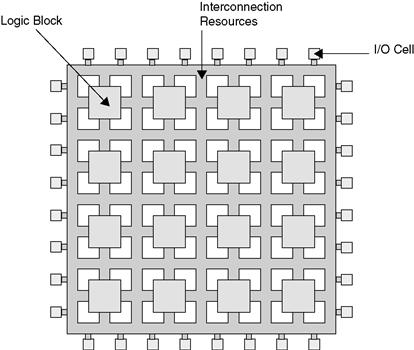
Figure 29.1 FPGA architecture
The important thing to note about the FPGA architecture is its regular, ASIC-like structure. This regular structure makes FPGAs useful for all kinds of logic designs.
29.2 Configurable Logic Blocks
Configurable logic blocks (CLBs) contain the programmable logic for the FPGA. The diagram in Figure 29.2 shows a typical CLB, containing RAM for creating arbitrary combinatorial logic functions. It also contains flip-flops for clocked storage elements and multiplexers in order to route the logic within the block and to route the logic to and from external resources. These muxes also allow polarity selection, reset input, and clear input selection.
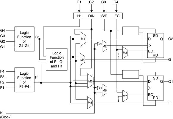
Figure 29.2 FPGA configurable logic block (CLB)
(courtesy of Xilinx Inc.)
On the left of the CLB are two 4-input memories, also known as 4-input lookup tables or 4-LUTs. As discussed in an earlier chapter, 4-input memories can produce any possible 4-input Boolean equation. Feeding the output of the two 4-LUTs into a 3-LUT, produces a wide variety of outputs (for up to nine inputs).
Four signals labeled C1 through C4 enter at the top of the CLB. These are inputs from other CLBs or I/O blocks on the chip, allowing outputs from other CLBs to be input to this particular CLB. These interconnect inputs allow designers to partition large logic functions among several CLBs. They also are the basis for connecting CLBs in order to create a large, functioning design.
The muxes throughout the CLB are programmed statically. In other words, when the FPGA is programmed, the select lines are set high or low and remain in that state. Some muxes allow signal paths through the chip to be programmed. For example, mux M1 is programmed so that the top right flip-flop data is either input C2, or the output of one of the two 4-LUTs or the output of the 3-LUT.
Some muxes are programmed to affect the operation of the CLB flip-flops. Mux M2 is programmed to allow the top flip-flop to transition on the rising or falling edge of the clock signal. Mux M3 is programmed to always enable the top flip-flop, or to enable only when input signal C4 is asserted to enable it.
Note that the clock input to the flip-flops must come only from the global clock signal. Earlier architectures allowed flip-flops to be clocked by the outputs of the combinatorial logic. This allowed asynchronous designs that created lots of problems, and FPGA vendors eventually took that capability out of their architectures, greatly reducing their headaches and greatly increasing the reliability of their customers’ designs.
Note that the logic outputs do not need to go through the flip-flops. Designers can use a CLB to create simple combinatorial logic. Because of this, multiple CLBs can, and often are, connected together to implement complex Boolean logic. This advantage of FPGAs over CPLDs means that designers can implement very complex logic by stringing together several CLBs. Unfortunately, routing delay in an FPGA is a significant amount of the overall delay. So this advantage also results in an overall decrease in the speed of the design.
Fine-Grained vs. Large-Grained CLBs
In theory, there are two types of CLBs, depending on the amount and type of logic that is contained within them. These two types are called large grain and fine grain.
In a large grain FPGA, the CLB contains larger functionality logic. For example, it can contain two or more flip-flops. A design that does not need many flip-flops will leave many of these flip-flops unused, poorly utilizing the logic resources in the CLBs and in the chip. A design that requires lots of combinatorial logic will be required to use up the LUTs in the CLBs while leaving the flip-flops untouched.
Fine grain FPGAs resemble ASIC gate arrays in that the CLBs contain only small, very basic elements such as NAND gates, NOR gates, etc. The philosophy is that small elements can be connected to make larger functions without wasting too much logic. If a flip-flop is needed, one can be constructed by connecting NAND gates. If it’s not needed, then the NAND gates can be used for other features. In theory, this apparent efficiency seemed to be an advantage. Also, because they more closely resembled ASICs, it seemed that any eventual conversion of the FPGA to ASIC would be easier.
However, one key fact renders the fine grain architecture less useful and less efficient. It turns out that routing resources are the bottleneck in any FPGA design in terms of utilization and speed. In other words, it is often difficult to connect CLBs together using the limited routing resources on the chip. Also, in an FPGA, unlike an ASIC, the majority of the delay comes from routing, not logic. Fine grain architectures require many more routing resources, which take up space and insert a large amount of delay, which can more than compensate for their better utilization. This is why all FPGA vendors currently use large grain architectures for their CLBs.
In the early days of the industry several FPGA manufacturers produced fine grain architectures for their devices. Thinking like ASIC vendors, they missed the significance of the routing issues. All of these vendors have either fallen by the wayside or have abandoned their fine grain architectures for large grain ones.
29.3 Configurable I/O Blocks
A configurable I/O block, shown in Figure 29.3, is used to bring signals onto the chip and send them back off again. The output buffer, B1, has programmable controls to make the buffer three-state or open collector and to control the slew rate. These controls allow the FPGA to output to most standard TTL or CMOS devices. The slew rate control is important in controlling noise, signal reflections, and overshoot and undershoot on today’s very fast parts. Slowing signal rise and fall times, reduces the noise in a system and reduces overshoot, undershoot, and reflections.
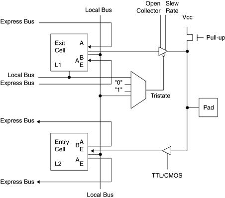
Figure 29.3 FPGA configurable I/O block
(courtesy of Xilinx Inc.)
The input buffer B2 can be programmed for different threshold voltages, typically TTL or CMOS level, in order to interface with TTL or CMOS devices. The combination of input and output buffers on each pin, and their programmability, means that each I/O block can be used for an input, an output, or a bidirectional signal.
The pull-up resistors in the I/O blocks are a nice feature. They take up little space in the FPGA and can be used to pull up three-state buses on a board. Floating buses increase the noise in a system, increase the power consumption, and have the potential to create metastability problems.
There are two small logic blocks in each I/O block, labeled L1 and L2 in the diagram. These blocks are there for two reasons. First, it always makes sense to stick logic wherever there is space for it. In the I/O block, there is space for it. Second, unlike an ASIC, the routing delay in an FPGA is much more significant than the logic delay. In an ASIC, signals are routed using metal layers, leading to RC delays that are insignificant with respect to the delay through logic gates. In an FPGA, the routing is done through programmed muxes in the case of SRAM-based devices and through conducting vias in the case of antifuse devices. Both of these structures add significant delay to a signal. The muxes have a gate delay associated with them. The conducting vias have a high resistance, causing an RC delay. I discuss this in further detail in Section 29.5.
Pull-Ups, Floating Buses, and Stubbornness
I would think it’s obvious to anyone who understands CMOS technology that floating buses are bad. CMOS devices dissipate power unnecessarily when the inputs are floating, and floating signals are more prone to noise. A pull-up resistor is a very simple, small, low-power, inexpensive solution to the problem of floating buses. In my career, though, I have encountered, on two occasions, a religious fervor about not putting pull-ups on potentially floating buses. I still don’t completely understand the reasons.
In one case, a career marketing manager at a large semiconductor company, who still prided himself on being a top-notch engineer, did a board design that I was asked to optimize, lay out, and debug. When I saw that he had omitted any pull-up resistors, I simply put them back in the schematic. When he saw this, he became angry. He told me that in all his years, he had never seen a problem, nor had he ever encountered a metastability problem. I replied that a reliability problem like metastability might only be seen once every year on a continually running board. It’s not something that can be measured. This manager went so far as to inform the layout designer to tell me that she couldn’t fit the pull-up resistor pack (nine pins on a small sliver of material) on the board. I could tell she felt ridiculous about this because she was telling me that she couldn’t do something that any fresh-out-of-school layout designer could accomplish with the cheapest layout software package available.
In the other case, I was brought in to do a sanity check of a board design that was nearing completion. A small startup had a contract to design some specialized network boards for Cisco Systems. A consultant had been hired to design the board, and the project manager then hired me to review the design. In my review, one of the potential problems I found was, yes, no pull-up resistors on the buses. I mentioned this casually, and the board designer became irate for the same reasons as the manager I had met. There was no reason for it. They were too expensive (actually about $.01 per resistor), and they took up too much space (a pack of ten resistors takes a few square millimeters). Finally he said, “We met with those guys at Cisco and they said the same thing. They wanted those stupid, unnecessary resistors on the buses. I just won’t waste my time doing it.” Later, in private, I talked with the project manager. “You may not think there’s a need for those resistors,” I said, “and you may not trust my judgment. But if I were selling boards to Cisco and they said to spread peanut butter on the boards, I’d break out the Skippy®.”
The point of these stories is that internal resistors on I/O pins of FPGAs make this problem go away. With internal resistors on the I/O pins, you can connect pull-ups to all of your buses, saving the tiny cost and area of a resistor pack, and no one will be the wiser.
Because of the large routing delays, if an input signal needed to be routed from an input buffer through internal interconnect to a flip-flop in a CLB inside the chip, as shown in Figure 29.4, there would be a large delay, labeled d, from the input pin to the data input of the flip-flop. In order to meet the hold time requirement of the internal flip-flop, labeled h, the hold time requirement for that signal with respect to the clock at the pins of the chip would be the sum of the delay d and hold time h which would be a large number and difficult to meet for devices interfacing with the FPGA. Instead, by placing flip-flops in the I/O blocks, the delay d is very small, resulting in a reasonable hold time at the pins of the chip.

Figure 29.4 Hold time issues in FPGAs
Similarly, if an output needed to be routed from a flip-flop in a CLB inside the device directly to an output buffer, as shown in Figure 29.5, there would be a large delay from the flip-flop output to the pin of the chip. This means that the clock-to-output delay for all signals would be the delay of the flip-flop, labeled c, plus the delay of the routing, labeled d. All chips interfacing with the FPGA would need to have a very small setup time requirement, or the clock speed of the system would need to be reduced. The solution is to have the output flip-flop inside the I/O block so that it is right next to the buffers. Then the routing delay is not significant. Having input and output flip-flops in the I/O blocks allows the FPGA and the system in which it is designed to be as fast as possible.

Figure 29.5 Setup time issues in FPGAs
29.4 Embedded Devices
Many newer FPGA architectures are incorporating complex devices inside their FPGAs. These devices can range from relatively simple functions, such as address decoders or multipliers, all the way through ALUs, DSPs, and microcontrollers and microprocessors. These embedded devices are optimized, and the FPGA devices that include them can offer you a very nice way of integrating an entire system onto a single chip, creating what is being called a system on a programmable chip or SOPC.
The advantage of FPGAs with embedded devices is that you can save board area and power consumption. You can usually save cost and increase system speed with these FPGAs. The embedded devices are already tested, just like a standalone chip, so that you don’t need to design the circuit from scratch and verify its functionality.
The disadvantage of these devices is that you tend to tie yourself into a single FPGA from a single FPGA vendor, losing some of the portability that engineers prefer. Each vendor has specific devices embedded into their FPGAs. In the case of embedded processors, each FPGA vendor usually licenses a specific processor core from a different processor manufacturer. This is good for the FPGA vendor because once they have a design win, that design is committed to their FPGA for some time. This is also a great way for the smaller FPGA vendors to differentiate themselves from the larger ones, by providing an embedded device that is in demand or soon will be, and can also produce a nice niche market for themselves that allows them to fend off eventual annihilation by the bigger vendors.
29.5 Programmable Interconnect
The interconnect of an FPGA is very different than that of a CPLD, but is rather similar to that of a gate array ASIC. Figure 29.6 shows the CLB’s hierarchy of interconnect resources. Each CLB is connected with the immediately neighboring CLBs, as shown in the top left. These connections are sometimes called short lines. (Note that for simplicity only the connections with CLB1 in the top left are shown. In reality, all four CLBs have connections to their nearest neighbors. These connections allow logic that is too complex to fit into a single CLB to be mapped to multiple CLBs.)

Figure 29.6 FPGA programmable interconnect
(courtesy of Xilinx Inc.)
Other routing resources consist of traces that pass by a number of CLBs before reaching switch matrices. These switch matrices allow a signal to be routed from one switch matrix to another to another, eventually connecting CLBs that can be relatively far from each other. The disadvantage to this method is that each trip through a switch matrix results in a significant delay. Often, in order to route signals through a chip, the routing delay becomes greater than the logic delay. This situation is unique to FPGAs and creates some design issues.
The third type of routing resource is the long line, which designers can use to connect critical CLBs that are physically far from each other on the chip without inducing much delay. These lines usually go from one end of the die to the other without connecting to a switch matrix. For critical path logic, long lines ensure that there will not be a significant delay.
The long line can also be used as buses within the chip. Three-state buffers are used to connect many CLBs to a long line, creating a bus. In an ASIC, three-state buses should be avoided because all three-state buses present a possible danger of contention or floating nodes, both of which can introduce long-term reliability problems if not designed carefully. Instead, muxes are used to combine many outputs because muxes are simple, easily expandable devices. In an ASIC, routing is not a significant problem. For an FPGA, though, muxes are not practical for connecting multiple outputs because this would require bringing outputs of different CLBs to a single CLB that contains the mux. Sometimes the CLBs producing the outputs are spread over a large section of the chip, requiring the signals to go through many switch matrices to reach the final destination. This introduces a very significant delay, slowing down the entire design.
Instead, CLBs near the long lines can directly drive the long lines with three-state drivers. The routing delay in this case is small. Of course, designers need to follow proper design techniques carefully to avoid any bus contention or floating buses.
Figure 29.7 shows a more detailed view of the routing for a single CLB. Note that the CLB has connections to local interconnect to connect it to neighboring CLBs. Also, it uses muxes to drive outputs onto the longer interconnects to connect it to devices at other parts of the chip. In this particular architecture, inputs from the interconnects go directly into the CLB, where the logic determines whether to use or ignore these signals.
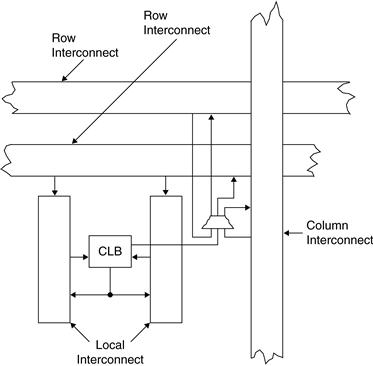
Figure 29.7 CLB programmable interconnect
(courtesy of Altera Corporation)
Note that CLBs themselves are often used for routing. In cases of high congestion on a chip, where routing resources are used up and not all signals and CLBs are connected, CLBs can be used for routing. In this case, the logic and muxes are set up so that a signal coming in simply goes out without any logical changes. This effectively increases routing resources in a densely packed design, but of course results in additional significant delay.
29.6 Clock Circuitry
Special I/O blocks with special high drive clock buffers, known as clock drivers, are distributed around the chip. These buffers are connected to clock input pins and drive the clock signals onto the global clock lines distributed throughout the device in a configuration called a clock tree. These clock lines are designed for low clock skew times and fast clock propagation times. Synchronous design is a must with FPGAs, because absolute skew times and delay times for signals cannot be guaranteed using the routing resources of the FPGA. Only when using clock signals from clock buffers can the relative delays and skew times be small and predictable.
29.7 SRAM vs. Antifuse Programming
There are two competing methods of programming FPGAs. The first, SRAM programming, involves static RAM bits as the programming elements. These bits can be combined in a single memory and used as a LUT to implement any kind of combinatorial logic, as described earlier. Also, programmers can use individual SRAM bits to control muxes, which select or deselect particular logic within a CLB, as described in Section 29.2. For routing, these bits can turn on a transistor that connects two traces in a switch matrix, or they can select the output of a mux that drives an interconnect line. Both methods are illustrated in Figure 29.8.

Figure 29.8 FPGA routing using SRAM bits
The other programming method involves antifuses. A regular fuse normally makes a connection until an excessive amount of current goes through it, generating heat and breaking the connection. With an antifuse, there is a small link between two conductors that are separated by an insulator, as shown in Figure 29.9. When a large voltage is applied across the link, the link melts. As the link melts, the conductor material migrates across the link, creating a conducting path between the two conductors. This process is used to connect traces inside the FPGA.
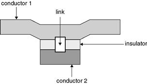
Figure 29.9 FPGA antifuses
(courtesy of Quicklogic Corporation)
There are two main types of antifuses in production today. In one type, conductor 1 is polysilicon, and conductor 2 is n+ diffused silicon. The insulator is oxide-nitride-oxide (ONO) and the link is composed of silicon.
In the second type of antifuse, both conductors are metal, the insulator is amorphous silicon, and the link is composed of titanium or tungsten silicide.
SRAM-based FPGAs have the advantage of being reprogrammable. Especially as FPGAs become larger and therefore more expensive, it is a nice feature during debugging to be able to reprogram them rather than toss out a bad design. SRAM-based FPGAs can also be reprogrammed while in the system, which makes in-field upgrading very easy. Programmers can alter a communication protocol or add a feature to the FPGA by a simple software change. SRAM-based FPGAs allow you to include small memories like FIFOs in your design, though large memories inside an FPGA are not cost effective. Also, SRAM-based FPGAs can be used for reconfigurable computing, a concept whereby computers contain FPGAs and algorithms can be compiled to run in the FPGAs.
A disadvantage of SRAM-based FPGAs is that they’re reprogrammable. Some applications, particularly military ones, often require that a device be nonvolatile and not susceptible to changes from radiation or power glitches. Antifuse FPGAs fit these criteria.
In theory, antifuse FPGAs are much faster than SRAM FPGAs. This is because antifuse FPGAs have a real connection between conductors for routing traces, as opposed to the logic or transistors used in SRAM-based FPGAs. Although the antifuse connections have a high resistance and therefore some RC delay associated with them, this delay should be much lower than the delay in SRAM-based FPGAs. You’ll notice that I use some wishy-washy terms here. The reason is that, in practice, antifuse FPGAs are not significantly faster than SRAM-based FPGAs, despite the theory. That’s because every semiconductor company in the world knows how to make SRAMs. It’s a standard product using a standard technology. Even companies that do not produce SRAMs often use SRAM structures to test their new processes because the structures are so regular and their performance is predicable. And because each semiconductor company is continually trying to improve its processes, they are always making faster and smaller SRAMs. On the other hand, only a small number of semiconductor companies, those manufacturing antifuse FPGAs, know how to make antifuses. There simply aren’t as many people or companies at work attempting to improve the yields, size, and speed of antifuses. For this reason, from a practical point of view, the speed difference between the two technologies is, and will probably remain, fairly small.
Antifuse FPGAs do have the advantage of lower power over SRAM-based FPGAs. Antifuse FPGAs also have an intellectual property security advantage. By this I mean that SRAM-based FPGAs must always be programmed by an external device upon power-up. It’s possible, then, for some unscrupulous engineer to copy your design simply by capturing the external bit stream. This engineer can then load the bit stream into any other FPGA, making a perfect copy of your design. Because an antifuse FPGA is programmed once, the program and the design are safe from prying eyes.
A newer technology that shows promise is Flash-based FPGAs. These devices are essentially the same as SRAM-based devices, except that they use Flash EPROM bits for programming. Flash EPROM bits tend to be small and fast. They are nonvolatile like antifuse, but reprogrammable like SRAM. Flash-based FPGA routing is shown in Figure 29.10.

Figure 29.10 FPGA routing using Flash bits
Table 29.1 summarizes how SRAM and antifuse programming technologies compare.
Table 29.1 Comparison of FPGA programming technolog
| SRAM | Antifuse | |
| Volatile | Yes | No |
| In-system programmable | Yes | No |
| Speed | Fast | Somewhat faster |
| Power consumption | Higher | Lower |
| Density | High | High |
| IP security | No | Yes |
| Embedded RAM | Yes | No |
29.8 Emulating and prototyping ASICs
Designers can also use FPGAs in places where an ASIC will eventually be used. For example, designers may use an FPGA in a design that needs to get to market quickly at a low initial development cost. Later, they can replace the FPGA with an ASIC when the production volume increases, in order to reduce the part cost. Most FPGA designs, however, are not intended to be replaced by an ASIC. FPGAs tend to be used where programmability, up-front cost, and time to market are more important than part cost, speed, or circuit density.
Reconfigurable Computing
An interesting concept, reconfigurable computing, has been floating around universities for the past decade or so and has been the subject of a number of research papers. In recent years, some companies have begun offering different variations of the concept in actual products. Essentially, the concept behind configurable computing is that computations can be performed much faster using special purpose hardware than using general-purpose hardware (a processor) running software. Therefore, general computing could be sped up significantly if hardware could be dynamically reconfigured to act as specialized coprocessors. Obviously, SRAM-based FPGAs would be an ideal implementation for this hardware.
The first, and most difficult, obstacle to reconfigurable computing is that a compiler must be able to partition a general-purpose computer program into software and hardware functionality by extracting the algorithms that can be implemented in hardware. It must then compile the algorithm code into an FPGA design. Synthesis programs have a difficult enough time doing the same operation using a hardware description language, which is designed specifically for this use. And a synthesis program doesn’t need to partition the code between hardware and software—all of the HDL code represents hardware. Because the process is so difficult, synthesis programs restrict the HDL code to a specific coding style to make the job easier. Also, hardware designers still need to set switches within comments in the code and change settings of the synthesis program, in order to get usable results. And after all of this, the designer often needs to tweak the HDL code to fit the design into the FPGA and to meet the required performance criteria.
The second obstacle is the relatively long time required to load a new design into an FPGA. Unless companies can speed up this process, reconfigurable computing will be limited to algorithms that are repeated in a loop in the code, so that the overhead of reprogramming the FPGA is compensated by the number of times the hardware algorithm is executed.
As companies come to market with reconfigurable computing solutions, they have been taking a more practical approach than the “Holy Grail” described above. Some of the solutions include libraries of algorithms that have already been developed, tested, and synthesized and that can be called from software. Other companies have created new programming languages that combine the flexibility of C++, for example, with an HDL. Such languages make it easier for compilers to partition and synthesize the code. The disadvantage is that these new nonstandard languages represent a particularly challenging learning hurdle, because they require a knowledge of both software and hardware design techniques.
I believe that these practical, but limited solutions will eventually produce a real-world product that will have some use in specific areas. The progress of reconfigurable computing will probably parallel that of silicon compilation. In the early 1980s, some companies, such as Silicon Compilers, Inc., were touting the ability to go directly from a schematic diagram to a chip layout. The problem turned out to be bigger than these advocates thought; the algorithms needed were much more complex than they originally believed, and the computing power to execute the algorithms just wasn’t available yet at a reasonable cost. So these companies all folded, but not without first producing corporate offspring and cousins, such as Synopsys Corporation, that decided they could tackle a much easier problem and still provide a solution that engineers could use. Their solution was software synthesis—software that could produce a gate level description from an RTL level description. This much less ambitious but much more achievable solution was a great success and may still eventually lead to the ultimate solution of silicon compilation. Many successful new products in the engineering design automation (EDA) industry follow this same trajectory. An ambitious first product fails, leading others to attempt smaller, less costly, more achievable products that succeed. In the same way, I believe, restricted solutions to reconfigurable computing will make their way into the marketplace and be successful, and eventually lead to more and more complex implementations.
There are two methodologies in integrated circuit chip design where FPGAs are being used to assist in the development of chips and the development of software that depends on these chips. These methodologies are known as emulation and prototyping.
29.8.1 Emulation
Several companies provide standalone hardware boxes for emulating the function of an ASIC or a custom integrated circuit. These hardware emulators can be programmed with a design for a chip. Once programmed, the emulator can be physically connected to a target circuit board where the chip would normally be connected. Then, the entire target system can be run as if the chip were actually available and functioning. You can then debug the design using real world hardware and real world software. You can stop and start the hardware emulator in order to examine internal nodes of the design. You can capture waveform traces of internal and I/O signals for debugging. You can make changes to the design to correct mistakes or to improve performance, before the design is committed to silicon.
For example, if you are designing a new microprocessor, you could load the microprocessor design into a hardware emulator, plug the emulator into a target personal computer motherboard, and actually boot Linux or any other operating system. You could even run real applications. Of course, a hardware emulator runs at a fraction of the speed of the final chip, but it affords a form of testing that is otherwise not possible, except with prototyping.
Different hardware emulators from different manufacturers have different internal architectures. Many of them, though, use large sets of FPGAs to emulate the chip design, because FPGAs allow users to easily load and modify designs, stop the design while it is in the system, and easily examine internal nodes and external I/O.
29.8.2 Prototyping
As FPGAs become faster and denser, and ASICs become larger, prototyping has become an important alternative to emulation. Prototyping involves loading a chip design into one or more FPGAs. If the chip design fits into a single FPGA, the FPGA can be plugged into a socket or soldered into a target circuit board where the final chip will ultimately go. The board can then be powered up and tested using real data. If the design cannot fit into a single FPGA, a board can be designed that contains several FPGAs into which the chip design is partitioned. Companies now provide software that will automatically partition a chip design into multiple FPGAs.
These design-specific FPGA prototypes generally run faster than a hardware emulator because they do not have the overhead required for a general-purpose machine, and there are fewer FPGAs—only the exact number required to implement your chip design. On the other hand, they do not have the built-in diagnostic capabilities of a hardware emulator, and they do not come with application engineers to support you. FPGA prototypes are generally cheaper than hardware emulators, but you must do all of the work, including partitioning the design, designing the board to hold the FPGAs, and designing whatever debug capabilities you require.
29.9 Summary
This section summarizes the various aspects of FPGAs that we have learned in this chapter. This section also provides a list of factors to use when deciding whether to choose a CPLD or FPGA for your design.
29.9.1 FPGA Selection Criteria
Knowledge of the internal architecture of FPGAs and the semiconductor technologies used to implement the programmable elements is critical for considering which FPGA to use in your design. When making that decision, you should take into account the following architectural and technological issues:
Configurable logic blocks — Although most FPGAs have similar logic blocks, there are differences, for example, in the number of flip-flops and the width of the lookup tables. Try to find a CLB architecture that fits your design. If your design has wide combinatorial functions, choose an FPGA using CLBs with large numbers of inputs. If your design has many pipelined stages, you will prefer CLBs with several flip-flops. Newer architectures are always being developed that fit the needs of specific types of designs, such as digital signal processing.
• The number of CLBs in the device — This will determine how much logic the device can hold and how easily your design will fit into it.
• The number and type of I/O pins — Obviously, the FPGA will need to support the number of I/O pins in your design. Also, determine how many of these are general-purpose I/O and how many are reserved for special functions such as clock input, master reset, etc.
• The number of clock input pins — Clock signals can be driven only into particular pins. If your design has several clock domains (i.e., sections driven by separate clocks), you will need an FPGA that has that many clock input pins.
• Embedded devices — Does your design interface with devices such as a microcontroller or a PLL? Many FPGAs now incorporate specialized functions like these, which will make your job much easier and allow you to integrate more devices into a single FPGA.
• Antifuse vs. SRAM programming — Which technology makes sense for your design? Do you need the speed, low power, nonvolatility, and security of an antifuse device, or do you need the reprogrammability of an SRAM-based device?
• Emulating and prototyping ASICs — FPGAs can be found in off-the-shelf hardware emulators for testing the design of an ASIC in a real-world target before it goes to silicon. Or you can use FPGAs to create your own custom prototype of an ASIC for the same kind of pre-silicon real-world testing.
29.9.2 Choosing Between CPLDs and FPGAs
Choosing between a CPLD and an FPGA will depend on the requirements of your project. Table 29.2 shows a summary of the characteristics of each type of programmable device. You will notice that I use fuzzy terms like “low,” “medium,” and “high” for some of the characteristics. People often want me to give a definitive answer on, for example, the number of gates in a typical CPLD or the cost of a typical FPGA. Because these numbers change so quickly, they are wrong as soon as they leave my lips (or in this case when they reach print). For that reason, I prefer to give relative characteristics that will still be correct for a while after I give them.
Table 29.2 CPLDs vs. FPGAs
| CPLD | FPGA | |
| Architecture | PAL-like | Gate array-like |
| Speed | Fast, predictable | Application dependent |
| Density | Low to medium | Medium to high |
| Interconnect | Crossbar | Routing |
| Power consumption | High per gate | Low per gate |
References
1. Logic Design Manual for ASICs. Santa Clara, CA: LSI Logic Corporation; 1989.
2. Davenport Jr, Wilbur B. Probability and Random Processes New York, NY: McGraw-Hill Book Company; 1970.
3. Dorf, Richard C, eds. Electrical Engineering Handbook Boca Raton, FL: CRC Press, Inc., 1993.
4. EDA Industry Working Groups. www.eda.org; Web site.
5. Maxfield, Clive. Max. Designus Maximus Unleashed! Woburn, MA: Butterworth-Heinemann; 1998.
6. Zeidman, Bob. Introduction to Verilog Piscataway, NJ: Institute of Electrical and Electronic Engineers; 2000.
7. Zeidman, Bob. Verilog Designer’s Library Upper Saddle River, NJ: Prentice-Hall, Inc., 1999.