
Chapter 25
EDA Design Tools for Analog and RF
They say a computer-based simulation of your analog circuit is important. This is because the use of your preferred computer Simulation Program with Integrated Circuit Emphasis (SPICE) program can reduce initial errors and development time. If you use your SPICE simulator correctly, you can drum out circuit errors and nuances before you go to your breadboard. In this manner, you will verify your design before you spend the time soldering your circuit. SPICE helps troubleshoot bench problems; it is a great place to try out different hypotheses. It is also great at “what if” scenarios (for example, exploratory design).
You can view the results from these software tools on a PC with user-friendly, graphical user interface (GUI) suites. This tool will fundamentally provide DC operating (quiescent) points, small signal (AC) gain, time domain behavior and DC sweeps. At a more sophisticated level, it will help you analyze harmonic distortion, noise power, gain sensitivity and perform pole-zero searches. This list is not complete, but generally, SPICE software manufacturers have many of these fundamental features available for the user. By finessing the Monte Carlo and worst-case analysis tools in SPICE, you can predict the yields of your final product. If you use your breadboard for this type of investigation, it could be very expensive and time consuming. All of these SPICE simulation advantages will speed up your application circuit time-to-market.
But, beware. You can effectively evaluate analog products if your SPICE models or macromodels are accurate enough for your application. The key words here are “accurate enough.” Such models, or macromodels, should reflect the actual performance of the component without carrying the burden of too many circuit details. Too many details can lead to convergence problems and extremely long simulation times. Not enough details can hide some of the intricacies of your circuit’s performance. Worse yet, your simulation, whether you use complete models or just macromodels, may give you a misrepresentation of what your circuit will really do. Remember that a SPICE simulation is simply a pile of mathematical equations that, hopefully, represent what your circuit will do. In essence, a computer product produces imaginary results.
So you might ask, “Why bother?” Is a SPICE simulation worth the time and effort? A pop quiz will help you clarify this question. The circuit in Figure 25.1 shows a fundamental, basic circuit. Is this circuit stable or does it oscillate? Would the output of the amplifier have an unacceptable ring? I would think that you would quickly look at this and say, “That is a silly question. Of course it is stable!” But then again, if you are always looking for the trick question you may be suspicious. So what is the answer?
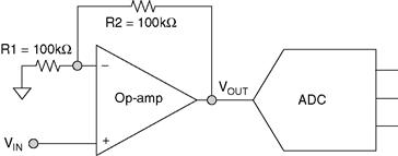
Figure 25.1 A variety of applications throughout the industry have this simple sub-circuit embedded in the system. This circuit simply takes an analog input signal and gains that signal to the output of the amplifier. For instance, an input signal of +1 VDC would become a +2 VDC signal at VOUT. The question is, would this DC signal oscillate? Or, would a 50 kHz sinusoidal signal oscillate or ring? The bandwidth of this amplifier is 2.8 MHz.
This simple amplifier circuit uses an amplifier in a gain of +2 V/V. The amplifier has a 100 kΩ resistor connected to its inverting-input to ground, and 100 kΩ resistor in the feedback loop. It would be easy to assume that this circuit is stable. However, tedious calculations will verify that this amplifier circuit will ring. This is due to the parasitic capacitances around the resistors and the high differential/common-mode capacitance of the amplifier’s input stage. For this particular amplifier, the input common-mode capacitance is 6 pF and the differential-mode capacitance is 3 pF. These capacitances interact with the feedback resistor causing a semi-unstable condition. If you bench-test this circuit, you will immediately see this condition on the oscilloscope. Parasitics on the breadboard will aggravate this instability.
For example, the 100 kΩ resistor in the feedback loop of the amplifier will also have approximately a parallel 0.5 pF parasitic capacitor (see Figure 25.2). This parasitic capacitance on the breadboard to ground could be as high as 2 pF or 3 pF. If you use the amplifier’s SPICE macromodel, with input impedances in the model and board parasitics, you will see this problem immediately in your simulation. If you breadboard the circuit, you most certainly will see this ringing.
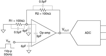
Figure 25.2 By enhancing the circuit diagram in Figure 25.1 with the parasitic capacitances of the resistors and amplifier, a simple of a circuit is not so simple. In the DC domain these capacitors will operate as open circuits. In the AC domain, the capacitors will affect the perfect square wave from the input to output. The perfect square wave will have quite a ring at the Vout node.
Changing the values of the two resistors in this circuit solves this problem. Hand calculations will help you find the correct values. A SPICE simulation will facilitate the process. This is a little easier than swapping out resistors on the breadboard until you find the right values. In SPICE, you can also look at the response of the amplifier using various resistors. This will help you find the “corner” of this oscillation. If you go back and change both values to 10 kΩ, you will have great success in SPICE and on the bench.
Figure 25.3. shows the simulation result.

Figure 25.3 You can quickly verify that this simple circuit will ring using a SPICE simulation. If you need to double-check this with a breadboard circuit, that is also a good idea, however, reducing the 100 kΩ resistors down to 10 kΩ resistors solves the problem. You do need to understand where the problem came from before you continue with your circuit design. But this simulation caught a significant stability problem. This ringing problem was an easy one to miss by inspection of the schematic.
In this chapter, we will discuss how to best determine if your SPICE simulation is telling you the truth. We do this by using three techniques. First, we will go through a short list of a few rules of thumb, which will help you examine the validity of your simulations; second, we will use common sense (at least where your circuit is concerned) when you first examine the results of your simulation; third, we will engage in an overview of what a macromodel can (or can’t) do for you. With this arsenal, you will be able to effectively use a SPICE simulation to weed out most of your circuit problems.
I’ll center the discussion on signal quality operational amplifiers. This is only because an amplifier is embedded somewhere in most purely analog circuits. I am going to leave it up to you to explore the remainder of analog macromodels, such as instrumentation amplifiers, difference amplifiers, references and so forth.
What won’t we cover in this chapter? I don’t intend to give you tips on how to use your favorite SPICE simulator tool. I’ll leave that topic up to your SPICE vendor and the numerous books on this topic. I also will not attempt to think for you by giving you cookbook answers to your problems. Rather, I am going to ask you to think through things yourself. Basically, you need to ask, “What do you expect from your circuit? Does your SPICE simulation match your expectations? Why or why not?”
The naysayers in the industry will tell you that your computer-based simulation tools will not work and using them will be a waste of time. These people are a bit misguided, and in my opinion have a superficial view of what this tool can really do. Sure, SPICE tools can lead you astray. But, like any tool, it is only as good as the user. Any insight that you gain from your simulations are provided if your SPICE tools are understood and used properly. Better yet, SPICE simulations will point out problems that you had never anticipated. In most cases, they use double-precision calculations. This makes it easier to detect low-level problems that are impossible to find on the bench. But step back and look at what you have. You very likely will have a simulation circuit that is built out of macromodels that are generated by various manufacturers of the products you are interested in using in your circuit.
The questions that bear asking are, “Does my model or macromodel simulate over temperature? Distortion? AC spec? Over process? Am I expecting the model to simulate these parameters? And to what degree of accuracy? What information do the macromodels I am using really provide?” The only way you can answer these questions is to have a feel for what your circuit will do (in real life), and ask challenging questions about your SPICE simulation results.
To give you a little taste of my experiences with SPICE, during one of my many lives, I was an analog IC designer. As a designer, I was using a transistor in an unorthodox manner. Mind you, my transistor models were the best that we had. My models were full-blown transistor-level models, designed to simulation the accurate behavior of my amplifier design. I was not using a macromodel substitution, but the “real” thing. I believed that a certain configuration of a transistor in the output stage would allow me to design a single-supply amplifier that could go nearly (within a few millivolts) to the negative rail. Although this type of circuit operation is not new today, in 1990 it had a degree of innovation. I arrived at this belief by examining and thinking through the circuit operation on paper. It was a very cool idea!
The simulation told me that there was no way my amplifier would even go near the negative rail. Therefore, I questioned my paper calculations and then the SPICE models. This exercise did not produce any answers, so I finally built the circuit on a breadboard. The tests from the breadboard circuit proved that my paper calculations were correct.
With this verification, I went back and created a special model for the culprit transistor in my circuit. I went to the bench to create the new transistor model, using a single transistor in a TO-99 package. This model was required because I was using the transistor in an unorthodox configuration. With those transistor changes, my amplifier circuit model did simulate the circuit accurately. At the “end-of-the-day,” I had all three tools in agreement. Modifying the transistor model did this. The problem could have been in my calculations or on the bench, but with these three votes, I was certain that I had a winner. The required three votes were the hand calculations, SPICE simulation and breadboard.
You probably will not dig into your circuits to this level of detail, however, the three steps to a successful, expeditious circuit design still hold true. These steps are: 1) Draw up the concept on paper, 2) Simulate your circuit to your satisfaction, 3) Breadboard critical portions of the circuit. All three of these steps are critical. Your SPICE simulations will not replace any of these steps; it will improve the likelihood of your success.
All of these steps were necessary:
1 Imagine what the circuit will do;
2 Simulate the circuit to match what you imagine it should do;
3 Breadboard the circuit and ensure the pencil design and simulation match. You need all three for a good level of confidence;
4 Adjust the model (or circuit) to match the three conditions (imagined operation, simulated operation and actual operation);
You might ask me why I bothered with this level of detail in my amplifier design project. Not only did I double-check the operation of the circuit using a breadboard circuit, but I also learned a lot about the nuances of the transistor through developing the new model. I found that the culprit transistor was quite useful. I was able to get the proper output-swing from my amplifier, and I used the same transistor configuration in other areas of my op-amp circuit. Not a waste of time for me! I gained a comfort level that is still paying me back. The product is still on the market, 14 years later.
The SPICE simulation tool is a good thing. It will help organize your thoughts and priorities. You can look for faults in terms of how you think the circuit or system will work versus reality. The best of all worlds is to have your tools point out where your mistakes are so you can initiate corrective actions to fix the circuit. The best place to find these problems is at the beginning of the design cycle, not the end. If you misunderstand the nuances of your circuit—that is, parasitics, you will find that your tools will tell you that all is well, when in fact it is not well at all.
25.1 The Old Pencil and Paper Design Process
The generation of your “pencil ‘n paper” circuit design is critical. Most likely, you will generate this circuit diagram using your SPICE software, but this is the stage where you take a good look at what you are trying to design. This is the time where you will develop an insider’s view of your circuit. In this stage of the design, you can labor through the mathematics of your circuit or better yet, hand-wave your way through the system. During this process, you should think about device and layout parasitics. You will also define the various circuit excitation parameters in preparation for your upcoming simulation.
We’ve all done the mathematical calculations of our designs in our good ‘ole school days. In those days, you boiled every part of the circuit down to a fundamental mathematical representation. However, the most important part of this stage is not the mathematics. In this stage, you should develop an intuition of what you think the circuit will do; then run some critical calculations in preparation for your next step, simulation. Hardware solutions (usually analog circuits) or firmware solutions (involving microprocessors, FPGAs or microcontrollers) require this process during the design phase. This technique is shown in Figure 25.4.
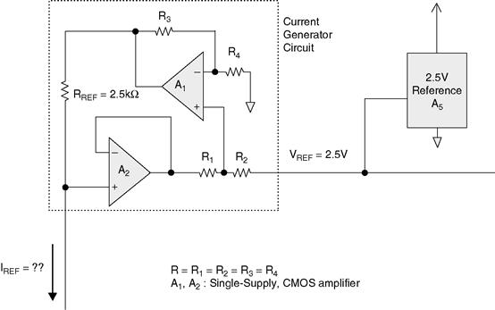
Figure 25.4 Sometimes a constant current source is required to excite a sensor in the system. This constant, floating current source contains a voltage reference, five resistors and two operational amplifiers. The fact that this current source is floating is a little tricky. This requires the pencil and paper evaluation as well as the breadboard. Conceptually, the noninverting input voltage of A2 is independent of the 2.5V reference (A5).
Figure 25.4 illustrates a floating-current-source circuit design. What I want to do with this circuit is to determine what the reference current (IREF) will be in relation to the reference voltage, A5. Conceptually, the current through R1 and R2 is equivalent. This assumes that the input current at the noninverting input of A1 is zero amps. If A1 is a CMOS-input amplifier, this is a pretty good assumption. The current through R1 and R2 can sink into A5 or source from A5. The voltage at the output of A2 can be higher or lower than the reference voltage of 2.5V. This is actually a good thing, because we did want a floating current source.
The voltage drop across the inputs of A1 is zero volts. If you are going to be exact, the voltage drop across these inputs is equal to the offset voltage of the amplifier, but we are going to let that go for now. The output voltage of A1 will be at least twice as high (if not higher) as the input voltage of that same amplifier. Since the reference for R4 is ground, the voltage of the output of A1 will always be equal to or greater than the voltage reference.
Since this is a floating supply, the best way to get a feel for the circuit is to assign an arbitrary voltage to a node and then work out the rest of the circuit. For example, if we assume the voltage at the noninverting input of A2 is equal to 0.5V, the voltage at the noninverting input of A1 is equal to 1.5V. Given this condition, the voltage at the output of A1 is 3.0V. Therefore, the voltage drop across the reference resistor, RREF, is 2.5V. If RREF is equal to 2.5 kΩ, the constant current source will be 1 mA.
That assumption took us a long way. It appears the impedance that IREF flows through determines the voltage at the noninverting input of A1. But, let’s not be too hasty. As an exercise for you, assume that the voltage at the noninverting input of A2 is equal to 3V. You will find that the voltage at the output of A1 is equal to 5.5V. You may notice that if you have a power supply voltage of 5V, this operation point is not possible. But, that is okay. Now we know most of the basics of this circuit. We also know the limits of the value of the resistor, RLOAD in Figure 25.5.

Figure 25.5 Hand-waving your way through a circuit will give you a good instinct about the circuit operation. As a final step, working through the calculations will validate your initial assumptions.
Figure 25.5 contains a summary of the calculations for this circuit. If you follow the logic in the formulas in this figure, the voltage at the output of A1 is equal to ½ the voltage at V1. The voltage at the noninverting input of A2 is equal to the voltage at the output of A1. This voltage is also equal to the reference voltage of A5 minus twice the difference between the reference voltage. The output of A2 is also equal to twice V1 minus the 2.5V reference of A5. The resistor value, R, is equal to 25 kΩ. This value ensures amplifier stability and to keep the output currents from the amplifiers relatively low.
Knowing this, you can determine the current through the reference resistor, RREF. Thevenin says that this current is equal to the voltage drop across RREF divided by RREF. We can calculate this voltage drop by using the earlier equations to equal 2.5V. As you work the real voltage and resistance values, you will summarize that the current through RREF is equal to 1 mA.
Now it is time to load the circuit. This circuit requires a low impedance load, such as a resistance temperature detector (RTD). If RLOAD is a PT100 RTD, it is equal to 100Ω at 0°C. In this the case, the voltage at the noninverting input of A2 is equal to 100 mV. Consequently, the voltage at the output of A2 is equal to 100 mV. In this application, the resistance range of the PT100 is 100Ω @ 0°C to 254Ω @ 400°C. At higher temperatures the output of A1 is equal to 2.754 mV. If the power supply voltage of the amplifiers is 5V, both amplifiers in this circuit are operating within their linear ranges.
The last steps in this portion of the process is to define the input signals, output representations of the signals, and parasitic resistances, capacitances or inductances that appear as a result of your layout of your circuit. The input signals would include transient signals in the time domain and AC signals in the frequency domain. The input signal definitions will be included at the front-end of your SPICE simulation listing. Further circuit examination will highlight the parasitic elements. For instance, the resistors in Figure 25.5 will have a parasitic capacitance (~0.5 pF) in parallel with the resistor element. Your layout may contribute additional capacitance in the ones of pico-farads because of the traces or wires that you are using. You need to determine if your PCB parasitics are an issue in your circuit. If they are, you need to quantify their values.
The stability of this circuit is another issue. Injecting a current spike with your upcoming SPICE simulator into a high impedance node, such as the inverting input of A2, will cause the circuit to ring if unstable. In the circuit in Figure 25.5, the parasitic capacitances of the resistors do not present a stability issue.
25.2 Is Your Simulation Fundamentally Valid?
Assuming you have worked through the “pencil ‘n paper” design of your circuit, you are ready to simulate. The output of this first design phase should be a circuit diagram as well as the operating points throughout the circuit. Defining the operating points of the initial, DC operating points and basic operation of the circuit over time is critical. The initial DC operating point should primarily provide the node voltages, but the current magnitudes of various portions of your circuit may also be important.
Once you finish designing your SPICE model, initiate your first simulation. At the conclusion of the simulation, you should first check the validity all of the operating points in your circuit. If you miss this step, you may be looking at erroneous AC or transient simulation data. The most critical initial DC operating points are the voltages throughout the circuit. For instance, verify that you have correct power supply connections. Then check to see that all of the DC voltages in your circuit are between the power-supply voltages. If any node in the DC operating points exceed your power-supply voltage, you probably have a bad connection in your circuit net list.
Figure 25.6 contains an example of several “red flags” in the DC operating points of the Figure 25.4 circuit. This listing initially shows the simulation circuit connections. Following the OP statement, the simulation listing calls out operational amplifier model (“ideal.mod”). Then there is a listing of the elements of the circuit, their associated device numbers and node assignments.

Figure 25.6 The first portion that you should inspect of any SPICE simulation is the DC operating points. You should check for appropriate voltage and currents in all of the elements of your circuit. This figure shows a portion of complete DC analysis. You will note that some of the nodes are negative values. Since this is a single-supply circuit, this is a warning that something is wrong.
Everything in this listing in Figure 25.6 looks in order to this point (unless you have already found the error). All of the amplifier nodes and resistor nodes are connected. The indication that something is wrong shows up in the NODE/VOLTAGE table. This is a SPICE generated table of simulation numbers. All of the nodes are present. You won’t recognize some of them because they are nodes that are internal to the two amplifier macromodels. You should immediately notice that there are negative voltages assigned to some nodes. It is a red flag that some of the negative nodes are internal in the amplifiers. This is a single-supply circuit. The supply voltages are ground and 5V.
If you return to the top of Figure 25.6 you will notice there is something peculiar with the op-amp, node assignments. The order of nodes versus function is:
That seems fine, but there is also a node called ns, and it is a ground connect for the rest of the circuit. There is the error. The amplifier-macromodel, negative-supply nodes attaches to ground. The schematic capture tool generated this error.
This is just one example of where the SPICE simulation can go wrong. If you continue with any type of analysis, such as AC or time transients, you will always wonder why the results look bad. Even worse, you will do what I did in the beginning of my career and assume that these types of bad results are true. A worse case scenario is to not look at the DC operating points at all. It always pays to question results and challenge the outcome. In a particular instance that I can recall, I chased my tail for most of the week only to find out that one of the nodes was not properly connected. If I had examined the DC analysis results, I would have immediately seen the problem. But, that is what experience is all about, right?
Another place you may want to look for the correctness of your DC analysis (or further on in the simulation) is places where the default values give you erroneous results. The OPTION statement of SPICE contains these default values that affect a variety of conditions. The OPTION statement sets all options, limits, and simulation analysis control parameters. The list of limits includes current accuracy, charge accuracy and the minimum conductance between branches, to name a few. It might be worth your time to look at this list. Usually these OPTION statement defaults won’t affect your simulation. However, an attitude that challenges the results of your SPICE simulation may bring errors into focus.
For instance, it may be critical to have the correct input-bias current values with a low-bias CMOS operational amplifier. An error in this parameter appears where your application circuit has high input impedances, such as a transimpedance amplifier or a low-pass filter. The SPICE program will insert a noiseless resistor inside components that have a discontinuity. The gate of the CMOS transistor is essentially floating, or not connected at DC. Although this node does have gate-to-source and gate-to drain capacitors, your SPICE will “view” this as an open circuit in the DC analysis. The SPICE software “fixes” this during the simulation by inserting a minimum conductance between discontinuous nodes.
In the SPICE macromodel in Figure 25.7, the input bias current of the CMOS transistor should be zero. Although, the ESD cells are not modeled here,they generate the input bias current of the amplifier. The “real” amplifier input CMOS transistors Q1 and Q2, will not generate gate current.
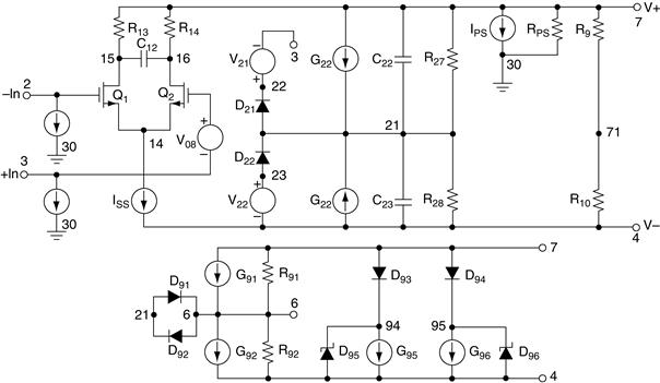
Figure 25.7 This is an example of a SPICE macromodel for a CMOS input amplifier. In this circuit, the SPICE simulation generates an input bias current error as an artifact of the SPICE constraints. Alexander and Bowers were the first to go public with this macromodel. This information appeared in the Electronic Design magazine in 1990.
In SPICE, the input or output current of the gates of these transistors is dependent on the voltage that appears across the gate-to-drain and gate-to-source nodes. This additional current is the SPICE default value, GMIN. The default value of GMIN is 1 × 10⁻¹² S (S = Siemens = 1/Ω). If inverted, this is equal to 1012 Ω. At first glance, this may not seem to be a problem. However, a voltage across that impedance will cause several picoamperes of error. A transimpedance amplifier (see Figure 25.8) is a circuit where this error will manifest itself as an output voltage error. To solve this problem, you can change the default value of GMIN or insert voltage-dependent- current-sources from the gate to ground of Q1 and Q2. As a note, when you change the default values through the OPTIONS statement, your changes will apply to the entire circuit simulation. Use this strategy with care. I prefer to make the changes to these defaults more local, which gives credence to the insertion of the voltage-dependent-current-sources over changing GMIN.

Figure 25.8 An amplifier with a low-input bias current in a transient-impedance amplifier circuit, like this one, is critical if you want to preserve reasonable accuracy. For this reason, CMOS or FET input amplifiers are preferred. If you try to simulate this circuit without the proper input bias current values, you will see an output voltage error at VOUT.
Figure 25.8 highlights this problem. In Figure 25.8, impinging light generates current from the photodiode. The current then flows through RF creating a voltage change at VOUT. The light source to the photodiode generates a low-level, full-scale current of several nano-amperes. If the light is not at full-scale, generating a lower current, the amplifier input bias current errors could cause voltage errors throughout the circuit.
Your DC analysis is the most important part of the validation of your SPICE simulation. If you take the time to meticulously perform this task you will have the confidence that the rest of you simulation has a good chance of being accurate (or as accurate as the simulation can be).
You should always challenge the validity of your SPICE simulation. If you know what to expect from your simulation, you can perform these challenges. If you plan to not evaluate your circuit and just “wait and see” what your SPICE simulation produces, there is a good chance that you will either chase your tail or go back to the pencil and paper evaluation. Either way, you will have wasted valuable time.
At this point, you may have noticed a small, nagging skepticism about SPICE simulations. Well, you are right. The simulation is only as good as your imaginary SPICE circuit. The fact that you place all of the components at the proper location in your circuit diagram and you are using the manufacturers approved macromodels may give you a false sense of security! Your simulations are only as good as your models. So, how are these models defined?
25.3 Macromodels: What Can They Do?
The concept of macromodels first came about in the 1970s. (“Macromodeling of Integrated Circuit Operational Amplifiers,” Graeme R. Boyle, Barry M. Cohn, Donald O. Pederson, James E. Solomon, IEEE Journal of Solid-state Circuits, Vol. SC-9, No. 6, December 1974, pp. 353–363.) These types of SPICE models provide a tool that reduces the system designer’s SPICE simulation time and convergence errors. It allows the designer to focus their efforts at a higher level of simulation. However, system designers, where there are many devices in the circuit, find macromodels very useful. Macromodels allow the SPICE user to simulate results successfully, in a timely fashion.
The engineers that develop IC semiconductors and use SPICE tools only use the macromodel during their circuit development to get proof of concept. They require more transistor-level detail inside their SPICE simulation when they look at the details of their integrated circuits. As the amplifier design process progresses to completion, the macromodel simplifies the transistor-level design too much for the IC designer. Contrary to popular belief, the IC designer’s models are also subject to discrepant behavior. There is no such thing as a 100% accurate SPICE model, whether it is a behavioral model, macromodel or transistor-level model.
A macromodel is actually a simple thing. On occasion, I have designed a few macromodels for existing ICs. The macromodel treats the device that you are trying to model like a black box. There are three general classes of simulation models. They are the behavioral model, the macromodel and the transistor-level model. The complexity of each of these types of models increases in the order of this list.
The behavioral model is closest to representing a “black box” with little or no relation to the actual device, except that it tries to emulate the real thing. The macromodel provides a circuit with more complexity. This type of model usually has the actual transistors on the input and output nodes. With this level of complexity, the model emulates the actual device more closely, but not completely.
In the interior of the macromodel, there are variety of dependent sources and independent sources. The most common dependent sources that are used are the linear voltage-controlled voltage source (VCVS), voltage-controlled current source (VCCS), current-controlled voltage source (CCVS), and the current-controlled current source (CCCS). Additionally, inside the macromodel there can be nonlinear dependent sources. The nonlinear dependent sources utilize a polynomial function in their definition. The macromodel’s author defines the coefficients of this polynomial. All of these sources attempt to emulate the actual performance of the device.
The transistor-level SPICE model includes all of the transistors, resistors and inductors of the actual device. Each of the elements has a SPICE model definition. Within each of these model definitions, the user can adjust various variables. For instance, the MOSFET SPICE model has 24 variables. With these variables, the SPICE user can adjust parameters such as lateral diffusion length, lateral diffusion width, zero-bias threshold voltage, transconductance coefficient and so forth.
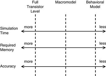
Figure 25.9 Transistor-level models are more complex than the macromodel or the behavioral model. Therefore, the transistor-level model will require more time to simulate and more computer memory. The increase in these requirements can make it difficult to complete a simulation, particularly if there are several transistor-level models in the simulation circuit. However, if you are able to tolerate longer simulation time, the transistor-level will produce results that are more accurate. In all three cases, the models are quite accurate for their intended application, and work poorly for other applications.
The transistor-level SPICE representation of the circuit is more complex than the behavioral model or the macromodel. Each of these levels has their place in your simulation strategy. The transistor SPICE model has more complexity and provides accuracy particularly for the IC designs. The transistor-level model details how the transistors in the circuit interact. This level of detail is not appropriate for the systems level designs. This type of design requires listings that can simulate several devices at one time. Under these conditions, the transistor-level models will be slower and less accurate. This is due to the increase in the node count of the entire simulation circuit.
Although the elements of a macromodel are complex, there are fewer elements in the total model listing. The overall complexity or sophistication of the macromodel is less than the transistor-level model. The macromodel simulates a list of specific parameters and no more. Many vendors will tell you what those parameters are in their SPICE macromodel listing. An example list of the parameters modeled for an operational amplifier would be: input voltage offset, DC PSRR, DC CMRR, input impedance, input bias current, open-loop gain, voltage ranges and supply current (typical performance at room temperature, 25°C).
A system-level simulation may include hundreds of building blocks. At this level it may be impossible to simulate in SPICE at the transistor or macromodel level. Even if these two levels of models do manage to give results, the system level simulation accuracy is much greater with correctly modeled behavioral building blocks. The transistor-level and macromodel complexity causes reduced accuracy in this environment and greater simulation time.
Consequently, the complete device model will consume more computer memory during simulation and take longer. If you simulate several device models at the same time, such as five or six transistor-level operational amplifiers, it is possible that the SPICE simulation will “crash” and not be able to complete the simulation of the circuit. Another setback that you will find with the transistor-level model is availability. Device vendors are very reluctant to provide the transistor-level models to their customers, or for that fact, anyone. This is because the transistor-level model contains proprietary information about their circuit. You can imagine that if a competitor got their hands on this type of model, the second source design work would be reduced significantly. This would make it easy for the competition to reverse-engineer a part and to quickly start stealing market share. More importantly, transistor-level models are less accurate for board and system level designs.
Figure 25.10 shows an example of an operational amplifier macromodel.

Figure 25.10 This PNP operational amplifier macromodel was originally designed in 1974 by Graeme R. Boyle, Barry M. Cohn, Donald O. Pederson, James E. Solomon. It was the first legitimate model published. Several other operational amplifier macromodel templates have been developed since then. Some SPICE vendors provide tools in their software to generate this type of macromodel.
The circuit in Figure 25.10 has some limitations. You will notice the ground connects in several places. Because of these ground connects, and the way they affect the macromodel’s behavior, the model will not operate in a single-supply environment. Figure 25.7 shows a model that is used in single-supply or in floating-supply environments. You should notice that in the operational amplifier input stages of the models in Figure 25.7 and Figure 25.10 have transistors. The input stage is the only place in these macromodels that have any resemblance to the actual device. With transistors inserted at this point, the model emulates the unique nonlinearities of the op-amp inputs. If you go beyond that stage, there is no longer a resemblance between the actual transistor-level model and these macromodels. The creator of the final model in Figure 25.7 and Figure 25.10 uses the dependent current and voltage sources to produce the real amplifier behavior. Keep in mind, the objective of the macromodel is not to copy the transistor model, but to imitate the operation of the device. In particular, the amplifier macromodel imitates the amplifier’s operation in applications, and not as a stand-alone model.
With all of these issues in mind, it is easy to understand that macromodels do not produce the complete performance of the actual amplifier circuit. The more simplistic models are able to simulate a limited number of the amplifier attributes. For example, in its most basic form, the macromodel illustrated in Figure 25.10 will only provide a small subset of the amplifier’s attributes. This macromodel models the input bias current and input impedance. It does not model the input rail-to-rail swing very accurately. The output characteristics that this macromodel can simulate are output current limit, output resistance and output voltage swing.
The output-voltage swing limits are set as if the amplifier is in a comparator configuration. This macromodel will not assist in demonstrating the nonlinear behavior of the output stage as the output gets close the rails. The macromodel’s attributes in the AC domain include gain versus frequency, phase versus frequency and a symmetrical slew rate. This macromodel will not reproduce a real amplifier’s asymmetrical (low to high, high to low) slew rate. Finally, the macromodel accurately reflects the DC quiescent current in a simulation. If the output of the amplifier is loaded and exercised, the current required will be pulled from ground and not from the power supplies. All of these performance attributes are only good at room temperature, or 25°C.
Enhancements that are added by the vendor to this limited list of attributes are offset voltage at room temperature, input noise and input offset current.
Most vendors design their macromodels to produce typical performance attributes and they don’t reflect the minimums and maximums you will find in the data sheet. If you want the macromodel to show you the amplifier’s operation with minimum or maximum performance specifications, you will have to proceed with caution and tweak the macromodel yourself. As a final shortcoming of this type of macromodel, these simulation attributes do not change as the real amplifier would if you were to vary the simulation temperature.
The model shown in Figure 25.10 is less flexible than the model shown in Figure 25.7. The model in Figure 25.7 overcomes quite a few limitations found in the model in Figure 25.10. For example, it is possible to use this macromodel for single-supply amplifiers. In addition, the output current in Figure 25.7 flows from the power supplies rather than the ground connect. Such attributes as power supply reduction (PSRR) and common-mode rejection (CMRR) ratios are included in this model. This model also lends itself to easily include over-temperature attributes.
The long and short of this discussion is that the capability of every macromodel is dependent on the whims of the macromodel designer. Figure 25.11 has a short list of a few amplifier macromodels that have various levels of capability.
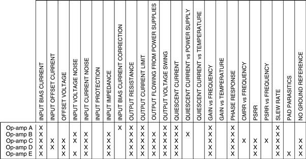
Figure 25.11 The capability of the amplifier macromodel varies from author to author and vendor to vendor. The best line of defense is to find out what your macromodel can or can’t do before you use it in your simulation. You can determine this by asking the vendor for that information, or by running your own tests in SPICE to determine what the macromodel’s capabilities are.
Computer-based simulations can significantly reduce the development time and therefore speed up the time-to-market of your designs. These facts alone make SPICE simulations attractive to the IC designer as well as the systems designer. With the increasing use of SPICE-based simulations, there is also a rising demand for accurate models. The expectation is that your models, or macromodels, reflect the actual performance of the component. This should be done without carrying the burden of too many circuit details. Companies in industry have responded to this need by providing macromodels for a broad range of products. The selection of SPICE macromodels from these companies ranges from op-amp, difference amps, instrumentation amps, isolation amps, to analog function circuits.
Analog manufacturers will also provide other tools that will facilitate your design process. An analog filter’s design tools are the most prevalent. Some of the tools allow the designer to use any manufacturers’ devices in the circuit while others require that the user use only their products. Another popular tool can help you with power supply design. In this case, the manufacturer controls the selection of the devices that will work in the circuits that their tool creates. They do this by knowing the particulars of their products and assisting design-in for their products.
25.4 VHDL-AMS
With the increasingly high level of system integration it is becoming necessary to model not only electronic behavior of systems, but also interfaces to ‘real-world’ applications and the detailed physical behavior of elements of the system in question. The emergence of standard languages such as VHDL-AMS has made it possible to now describe a variety of physical systems using a single design approach and simulate a complete system. Application areas where this is becoming increasingly important include mixed-signal electronics, electro-magnetic interfaces, integrated thermal modeling, electro-mechanical and mechanical systems (including micro-electro-mechanical systems, MEMS), fluidics (including hydraulics and microfluidics), power electronics with digital control and sensors of various kinds.
In this section, we will show how the behavioral modeling of multiple energy domains is achieved using VHDL-AMS, demonstrating with the use of examples how the interactions between domains takes place, and provide an insight into design techniques for a variety of these disciplines. The basic framework is described, showing how standard packages can define a coherent basis for a wide range of models, and specific examples used to illustrate the practical details of such an approach. Examples such as integrated simulation of power electronics systems including electrical, magnetic and thermal effects, mixed-domain electronics and mechanical systems are presented to demonstrate the key concepts involved in multiple energy domain behavioral modeling.
The basic approach for modeling devices in VHDL-AMS is to define a model entity and architecture(s). The model entity defines the interface of the model to the system and includes connection points and parameters. A number of architectures can be associated with an entity to describe the model behavior such as a behavioral or a physical level description. A complete model consists of a single entity combined with a single architecture. The domain or technology type of the model is defined by the type of terminal used in the entity declaration of the ports. The IEEE Std 1076.1.1 defines standard types for multiple energy domains including electrical, thermal, magnetic, mechanical and radiant systems. Within the architecture of the model, each energy domain type has a defined set of through and across variables (in the electrical domain these are voltage and current, respectively) that can be used to define the relationship between the model interface pins and the internal behavior of the model.
In the ‘conventional’ electronics arena, the nature of the VHDL-AMS language is designed to support ‘mixed-signal’ systems (containing digital elements, analog elements and the boundary between them) with a focus on IC design. Where the strengths of the VHDL-AMS language have really become apparent, however, is in the multi-disciplinary areas of mechatronic and MEMS. In this chapter, I have highlighted several interesting examples that illustrate the strengths of this modeling approach, with emphasis on multiple domain simulations.
25.4.1 Introduction to VHDL-AMS
VHDL-AMS is a set of analog extensions to standard digital VHDL to allow mixed-signal modeling of systems. The VHDL-AMS language was approved as IEEE Std 1076.1 in 1999; however, it is important to note that IEEE 1076.1-1999 encompasses the complete digital VHDL 1076 standard and is not a subset.
The standard does not specify any libraries for analog disciplines (e.g., electrical, mechanical, etc.). This is a separate exercise and is covered by a subset working group IEEE 1076.1.1, which was released as an IEEE Std 1076.1.1 in 2004.
In order to put the extensions into context it is useful to show the scope of VHDL, and then VHDL-AMS alongside it and this is shown in Figure 25.12.

Figure 25.12 Scope of VHDL-AMS
The key extensions for VHDL-AMS is the ability to look upward to transfer functions (behavioral and in the Laplace domain) and downward to differential equations at the circuit level.
The extensions to VHDL for VHDL-AMS can be summarized as follows:
1 A new type of ports called TERMINALS—basically analog pins.
2 A new type of TYPE called a NATURE that defines the relationship between analog pins and variables.
3 A new type of variable called a QUANTITY that is an analog variable.
4 A new type of variable assignment that is used to define analog equations that are solved simultaneously.
5 Differential equation operators for derivative (‘DOT) and integration (‘INTEG) with respect to time.
6 IF statements for equations (IF USE).
7 Break statement to initialize the nonlinear solver.
8 STEP LIMIT control for limiting the analog time step in the solver.
25.4.2 Analog Pins: TERMINALS
In order to define analog pins in VHDL-AMS we need to use the TERMINAL keyword in a standard entity PORT declaration. For example, if we have a two pins device that has two analog pins (of type electrical, more on this later), then the entity would have the basic form as shown below:
Notice that as the VHDL-AMS extensions are defined as an IEEE standard, then the use of a standard library such as electrical pins requires the use of the electrical_systems.all; packages from the IEEE library.
Notice that the pins do not have a direction assigned as analog pins are part of a conserved energy system and are therefore solved simultaneously.
25.4.3 Mixed-Domain Modeling
In order to use standard models, there has to be a framework for terminals and variables which is where the standard packages are used. There is a complete IEEE Std (1076.1.1) which defines the standard packages in their entirety; however, it is useful to look at a simplified package (electrical systems in this case) to see how the package is put together.
For example, electrical systems models need to be able to handle several key aspects:
The electrical systems ‘package’ needs to encompass these elements.
First, the basic subtypes need to be defined. In ALL the analog systems and types, the basic underlying VHDL type is always REAL, and so the voltage and current must be defined as subtypes of REAL:
Notice that there is no automatic unit assignment for either, but this is handled separately by the UNIT and SYMBOL attributes in IEEE Std 1076.1.1. For example, for voltage the unit is defined as “Volt” and the symbol is defined as “V”.
The remainder of the basic electrical type definition then links these subtypes to the through and across variable of the type, respectively:
25.4.4 Analog Variables: Quantities
Quantities are purely analog variables and can be defined in one of three ways. Free quantities are simply analog variables that do not have a relationship with a conserved energy system. Branch quantities have a direct relationship between one or more analog terminals and finally source quantities are used to define special source functions (such as AC sources or noise sources).
For example to define a simple analog variable called x, that is a voltage (but not related directly to an electrical connection (TERMINAL), then the following VHDL could be used:
On the other hand, a branch between two electrical pins has a through variable (current) and an across variable (voltage) and this requires a “branch” quantity so that the complete description can be solved simultaneously. For example, the complete quantity declaration for the voltage (v) and current (i) of a component between two pins (p & m) could be defined as:
25.4.5 Simultaneous Equations in VHDL-AMS
In VHDL-AMS the equations are analog and solved simultaneously, which is in contrast to signals that are solved concurrently using logic techniques and variables which are evaluated sequentially. For example in VHDL-AMS to solve an equation use the ‘= =’ operator:
where both Y and X have to be defined as real numbers (quantities or other VHDL variable types).
25.4.6 A VHDL-AMS Example
25.4.6.1 A DC Voltage Source
In order to illustrate some of these basic concepts consider a simple example of a DC voltage source. This has two electrical pins p & m, and a single parameter dc_value that is used to define the output voltage of the source (Figure 25.13).

Figure 25.13 Basic voltage source
This can be modeled in VHDL-AMS in two parts, the entity and architecture. First, consider the entity. This has two electrical pins, so we need to use the ieee.electrical_systems.all; package and therefore the ports are to be declared as TERMINALS. Also the generic de_value must be defined as a real number with the default value also defined as a real number (e.g., 1.0):
The architecture must define the quantities for voltage and current through the source and then link those to the terminal pin names. Also, the output equation of the source must be modeled as an analog equation in VHDL-AMS using the ‘= =’ operator to implement the function v = dc_value:
25.4.6.2 Resistor
In the case of the resistor, the basic entity is very similar to the voltage source with two electrical pins p & m with a single generic, this time for the nominal resistance rnom (Figure 25.14).

Figure 25.14 VHDL-AMS resistor symbol
This can be modeled in VHDL-AMS in two parts, the entity and architecture. First consider the entity. This has two electrical pins, so we need to use the ieee.electrical_systems.all; package and therefore the ports are to be declared as TERMINALS. Also the generic rnom must be defined as a real number with the default value also defined as a real number (e.g. 1000.0):
The architecture must define the quantities for voltage and current through the resistor and then link those to the terminal pin names.
Also, the output equation of resistor must be modeled as an analog equation in VHDL-AMS using the ‘= =’ operator to implement the function v = I * rnom:
25.4.7 Differential Equations in VHDL-AMS
VHDL-AMS also allows the modeling of linear differential equations using the two differential operators:
We can illustrate this by taking two examples, a capacitor and an inductor. First, consider the basic equation of a capacitor:
![]()
Using a similar model structure as the resistor, we can define a model entity and architecture, but what about the equation? In VHDL-AMS, the ‘DOT operator is used on the voltage to represent the differentiation as follows:
Therefore, a complete capacitor model in VHDL-AMS could be implemented as follows:
USE IEEE.ELECTRICAL_SYSTEMS.ALL;
ARCHITECTURE simple OF capacitor IS
What about an inductor? The basic equation for an inductor is given below:

Obviously, the most direct way to implement this equation would be to use the ‘INTEG operator, however care should be taken with the integration operator.
Obviously, the initial condition must be considered and in addition different implementations can occur across simulators. However, the resulting implementation in its simplest form could be as follows:
25.4.8 Mixed-Signal Modeling with VHDL-AMS
Most design engineers are familiar with the concepts of “digital” or “analog” modeling; however, a true understanding of “mixed-signal” modeling is often lacking. In order to explain the term mixed-signal modeling, it is necessary to review what we mean by analog and digital modeling first. First, consider digital modeling techniques.
Digital systems can be modeled using digital gates or events. This is a fast way of simulating digital systems structurally and is based on VHDL or Verilog gate level models. Digital simulation with digital computers relies on an event-based approach, so rather than solve differential equations, events are scheduled at certain points in time, with discrete changes in level. The resolution of multiple events and connections is achieved using logic methods. The digital models are usually gates, or logic based and the resulting simulation waveforms are of fixed, predefined levels (such as “0” or “1”). Also, “instantaneous” changes can take place, that is the state can change from ‘0’ to ‘1’ with zero risetime.
In the analog world, in contrast, the lowest level of detail in practical electrical system design is the use of analog equation models in an analog simulator—the benchmark of this approach is historically the SPICE simulator. In many cases the circuit is extracted in the form of a netlist. The netlist is a list of the components in the design, their connection points and any parameters (such as length, width or scaling) that customize the individual devices.
Each device is modeled using nonlinear differential equations that must be solved using a Newton-Raphson type approach. This approach can be very accurate, but is also fraught with problems such as:
• Convergence: If the model does not converge, then the simulation will not give any meaningful result or fail altogether.
• Oscillation: If there are discontinuities, the solution may be impossible to find.
• Time: The simulations can take hours to complete, days for large designs with detailed device models.
In the analog domain the Newton-Raphson approach is generally used to find a solution which relies on calculating the derivatives as well as the function value to obtain the next solution. The basic Newton-Raphson method for nonlinear equations is defined as:
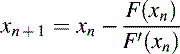
F(xn) and F′(xn) must be explicitly known and coded into the simulator (for SPICE) and this gives an approximate solution to the exact problem. For VHDL-AMS simulators the derivatives must be estimated using a Secant method (or similar) (Figure 25.15).

Figure 25.15 Newton-Raphson Method
So given these diametrically opposed methods, how can we put them together? What about mixed-signal systems? In these cases, there is a mixture of continuous analog variables and digital events. The models need to be able to represent the boundaries and transitions between these different domains effectively and efficiently. The basic mechanism to checking if an analog variable crosses a threshold is to use the ABOVE operator in VHDL-AMS.
For example, to check if a voltage “vin” is above 1.0V, the following VHDL-AMS could be used:
This can be extended to use parameters in the model—say a threshold voltage parameter (vth)—defined previously as a generic or constant:
Notice that flag is a signal and is therefore able to be used in the sensitivity list to a process enabling digital behavior to be triggered when the threshold is crossed. If the opposite condition is required, that is BELOW the threshold, then the condition is simply inverted using the NOT operator:
The digital-to-analog interface is slightly more complex than the analog-to-digital interface inasmuch as the output variable needs to be controlled in the analog domain.
When a digital event changes (this can be easily monitored by a sensitivity list in a process) the analog variable needs to have the correct value and the correct rate of change. To achieve this we use the RAMP attribute in VHDL-AMS.
Consider a simple example of a digital-logic-to-analog-voltage interface:
This can be implemented using VHDL-AMS as follows:
Clearly, there will be problems with this simplistic interface as the transition of vout will be instantaneous—causing potential convergence problems. The technique to solve this problem is to introduce a RAMP on the definition of the value of vout with a transition time to change continuously from one value to another:
where tt (the transition time) is defined as a real number (e.g., tt : real : = 1.0e = – 9;).
An alternative to the specific transition time definition is to limit the slew rate using the SLEW operator. The technique to solve this problem is to introduce a slew rate definition on the definition of the value of vout with a transition time to change continuously from one value to another:
where max_slew_rate is defined as a real number (e.g., max_slew_rate : real : = 1.0e6;).
25.4.9 A basic switch model
Consider a simple digitally controlled switch that has the following characteristics:
Using this simple outline a basic switch model can be created in VHDL-AMS. The entity is given below:
USE ieee.electrical_system.ALL;
GENERIC ( ron : real := 0.1;– On resistance
roff : real := 1.0e6; – Off resistance
ton : real := 1.0e-6; – turn on time
The basic structure of the architecture requires that the voltage and current across the terminals of the switch be dependent on the effective resistance of the switch (reff):
The process waits for changes on the input digital signal (d) and schedules a signal r_eff to take the value of the effective resistance (ron or roff) depending on the logic value of the input signal. The VHDL for this functionality is shown below:
When the signal r_eff changes, then this must be linked to the analog quantity reff using the ramp function. Previously we showed how the ramp could define a risetime, but in fact it can also define a falltime. Implementing this in the switch model architecture we get the following VHDL-AMS:
The complete VHDL-AMS model for the switch is given below:
25.4.10 Basic VHDL-AMS Comparator Model
Consider a simple comparator that has two electrical inputs (p & m), an electrical ground (gnd) and a digital output (d). The comparator has a digital output of “1“when p is greater than m and “0” otherwise (Figure 25.16).
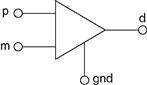
Figure 25.16 Comparator
The entity defines the terminals (p, m, gnd), digital output (d), input hysteresis (hys) and the propagation delay (td):
The first step in the architecture is to define the input voltage and basic process structure:
architecture simple of comparator is
constant vh : real := ABS(hys)/2.0;
constant vl : real := -ABS(hys)/2.0;
The quantity vin is defined as the voltage across the input pins p and m:
Notice that no current is defined, assumed to be zero, so there is no input current to the comparator. Also notice that there is no input voltage offset defined—this could be added as a refinement to the model later. The process defines the upper and lower thresholds (vh and vl) based on the hysteresis:
The process then defines a wait statement checking vin for crossing either of those threshold values:
The final part of the process is to add the digital output logic state dependent on the threshold status of vin:
The output state (d) is then scheduled after the delay time defined by td.
The completed architecture is shown below:
25.4.11 Multiple Domain Modeling
A final significant application area for VHDL-AMS has been the modeling of electro-mechanical systems, particularly micromachines (or MEMS). Exactly the same principles are used for these devices, with the mechanical domain models defined as required for the mechanical equations. It is worth noting that the mechanical models are divided into rotational (angular velocity and torque) and translational (force and distance) types. A typical simple example of a mixed-domain system is a motor, in this case a simple DC motor. Taking the standard motor equations as shown below, it can be seen that the parameter ke links the rotor speed to the electrical domain (back emf) and the parameter kt links the current to the torque:

25.4.12 Summary
It has become crucial for effective design of integrated systems, whether on a macro- or microscopic scale, to accurately predict the behavior of such systems prior to manufacture. Whether it is ensuring that sensors or actuators operate correctly, or integrated components such as magnetics also operate correctly, or analyzing the effect of parasitics and nonideal effects such as temperature, losses and nonlinearities, the requirement for multiple domain modeling has never been greater.
Now languages such as VHDL-AMS offer an effective and efficient route for engineers to describe these systems and effects, with the added benefit of standardization leading to interoperability and model exchange. The challenge for the EDA industry is to provide adequate simulation and particularly modeling tools to support engineering design.
The opportunity for field-programmable gate array (FPGA) designers is to take advantage of this huge advance in modeling technology and use it to make sure that digital controllers and designs can operate effectively and robustly in real-world applications.
References
1. Nilsson Riedel. Introduction to Pspice Manual for Electronic Circuits Using OrCad Release 9.1 Prentice-Hall 2000.
2. Kielkowski Ron M. Inside SPICE: Overcoming the Obstacles of Circuit Simulation McGraw Hill 1994.
3. Choi Pyung, Connelly J Alvin. Macromodeling with SPICE Prentice-Hall 1992.
4. Baker Bonnie C. Spice Models Low-bias Op Amps Correctly. EDN Magazine 1992.
5. Boyle Graeme R, Cohn Barry M, Pederson Donald O, Solomon James E. Macromodeling of Integrated Circuit Operational Amplifiers. IEEE Journal of Solid-State Circuits. 1992;SC-9(6):353–363.
6. Alexander Bowers. Designer’s Guide to Spice-Compatible Op-amp Macromodels — Part 1. Electronic Design News. 1990;Volume 35.
7. Antognetti Massobrio. Semiconductor Device Modeling with Spice McGraw Hill 1980.
Useful texts for VHDL Digital Systems Design
Digital System Design with VHDL by Mark Zwolinski, published by Pearson Education, is a superb introduction to designing with VHDL. It is used in many universities worldwide for teaching VHDL at an undergraduate level and has numerous basic examples to enable a student to get started. I would also recommend this to an engineer getting started with VHDL.
The Designers Guide to VHDL
The Designers Guide to VHDL by Peter Ashenden is perhaps the most comprehensive book on VHDL from a variety of perspectives. It covers the syntax and language rigorously, has plenty of examples, and is a great desk top reference book. For nonbeginners in VHDL, this is the book I would recommend.
VHDL: Analysis and Modeling of Digital Systems
VHDL: Analysis and Modeling of Digital Systems (McGraw-Hill Series in Electrical and Computer Engineering) by Zainalabedin Navabi is a detailed look at not only how VHDL can be used to model digital systems, but many of the detailed issues regarding timing and analysis that are often skipped over by other texts on VHDL. It is perhaps not a beginner’s book, but is especially useful for those who require a deeper understanding of issues relating to timing.
VHDL for Logic Synthesis
VHDL for Logic Synthesis by Andrew Rushton, published by Wiley, is a useful background text for those who perhaps need to understand how VHDL can be used for practical synthesis. The book discusses what and what is not synthesizable and also explains how some useful and somewhat arcane VHDL functions operate.