
Chapter 19
Op-Amps
19.1 The Magical Mysterious Op-Amp
An operational amplifier, often called an op-amp, in my opinion, are probably the misunderstood, yet potentially useful IC at the engineer’s disposal. It makes sense that if you can understand this device you can put it to use, giving you a great advantage in designing successful products.
19.1.1 What is an Op-Amp Really?
Do you understand how an op-amp works? Would you believe that op-amps were designed to make it easier to create a circuit? You probably didn’t think that the last time you were puzzling over a misbehaving breadboard in the lab.
In today’s digital world, it seems to be common practice to breeze over the topic of op-amps giving the student a dusting of commonly used formulas without really explaining the purpose or theory behind them. Then, the first time an engineer designs an op-amp circuit, the result is utter confusion when the circuit doesn’t work as expected. This discussion is intended to give some insight into the guts of an operational amplifier, and to give the reader an intuitive understanding of op-amps.
One last point—make sure you read this section first! It is my opinion that one of the causes of op-fusion (op-amp confusion) as I like to call it, is that the theory is taught out of order. There is a very specific order to this, so please understand each section before moving on.
First, let’s take the symbol of an op-amp (Figure 19.1).
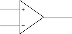
Figure 19.1 Your basic op-amp
There are two inputs, one positive and one negative, identified by the + and − signs.
There is one output.
The inputs are high impedance. I repeat. The inputs are high impedance. Let me say that one more time. THE INPUTS ARE HIGH IMPEDANCE! This means they have (virtually) no effect on the circuit to which they are attached. Write this down, as it is very important. We will talk about this in more detail later. This important fact is commonly forgotten and contributes to the confusion I mentioned earlier.
The output is low impedance. For most analysis it is best to consider it a voltage source.
Now let’s represent the op-amp with two separate symbols (Figure 19.2).
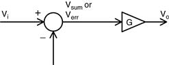
Figure 19.2 What is really inside an op-amp
You see here a summing block and an amplification block. You may remember similar symbols from your control theory class. Actually they are not just similar—they are exactly the same. Control theory works for op-amps. More on that later, too.
First, let’s discuss the summing block. You will notice that there is a positive input and a negative input on the summing block, just as on the op-amp. Recognize that the negative input is as if the voltage at that point is multiplied by a −1. Thus, if you have 1V at the positive input and 2V at the negative input, the output of this block is −1. The output of this block is the sum of the two inputs, where one of the inputs is multiplied by −1. It can also be thought of as the difference of the two inputs and represented by this equation: Vs = (V+) − (V−).
Now we come to the amplification block. The variable G inside this block represents the amount of amplification that the op-amp applies to the sum of the input voltages. This is also known as the open-loop gain of the op-amp. In this case, we will use a value of 50,000. You say, how can that be? The amplification circuit I just built with an op-amp doesn’t go that high! We will get to the amplification applications in a moment. Go find the open-loop gain in the manufacturer’s data sheet. This level of gain or even higher is typical of most op-amps.
Now for some analysis. What will happen at the output if you put 2V on the positive input and 3V on the negative input. I recommend that you actually try this on a breadboard. I want you to see that an op-amp can and will operate with different voltages at the inputs. However, a little math and some common sense will also show us what will happen. For example:
![]() (19.1)
(19.1)
Unless you have a 50,000V op-amp hooked up to a 50,000V bipolar supply, you won’t see −50,000V at the output. What will you see? Think about it a minute before you read on. The output will go to the minimum rail. In other words, it will try to go as negative as possible. This makes a lot of sense if you think about it like this. The output wants to go to −50,000V and obey the mathematics above. It can’t get there, so it will go as close as possible. The rails of an op-amp are like the rails of a train track—a train will stay within its rails if at all possible. Similarly, if an op-amp is forced outside its rails, disaster occurs and the proverbial magic smoke will be let out of the chip. The rail is the maximum and minimum voltage the op-amp can output. As you can intuit, this depends on the power supply and the output specifics of the op-amp.
OK, reverse the inputs. Now the following is true:
![]() (19.2)
(19.2)
What will happen now? The output will go to the maximum rail. How do you know where the output rails of the op-amp are? That depends on the power supply you are using and the specific op-amp. You will need to check the manufacturer’s data sheet for that information. Let’s assume we are using an LM324, with a +5V single-sided supply. In this case the output would get very close to 0V when trying to go negative and around 4V when trying to go positive.
At this time I would like to point something out. The inputs of the op-amp are NOT equal to each other. Many times I have seen engineers expect these inputs to be the same value. During the analysis stage, the designer comes up with currents going into the inputs of the device to make this happen (remember, high impedance inputs, virtually zero current flow). Then when he tries it out, he is confused by the fact that he can measure different voltages at the inputs.
In a special case, you can make the assumption that these inputs are equal. It is NOT the general case. This is a common misconception. You must not fall into this trap or you will not understand op-amps at all.
The examples above indicate a very neat application of op-amps: the comparator circuit. This is a great little circuit to convert from the analog world to the digital one. Using this circuit you can determine if one input signal is higher or lower than another. In fact, many microcontrollers use a comparator circuit in analog-to-digital conversion processes. Comparator circuits are in use all around us. How do you think the streetlight knows when it is dark enough to turn on? It uses a comparator circuit hooked up to a light sensor. How does a traffic light know when there is enough weight on the sensors to trigger a cycle to green? You can bet there is a comparator circuit in there.
Thumb Rules
• The inputs are high impedance; they have negligible effects on the circuit they are hooked to.
• The inputs can have different voltages applied to them; they do NOT have to be equal.
• The open-loop gain of an op-amp is VERY high.
• Due to the high open-loop gain and the output limitations of the op-amp, if one input is higher than the other the output will “rail” to its maximum or minimum value (this application is often called a comparator circuit).
19.1.2 Negative Feedback
If you didn’t just finish reading it, go back and read the thumb rules from the last section. They are very important to develop the correct understanding of what an op-amp does. Why are these points important? Let’s go over a little history. Up until the invention of op-amps, engineers were limited to the use of transistors in amplification circuits. The problem with transistors is that, being “current-driven” devices, they always affect the signal of the circuit that the designer wants to amplify by loading the circuit. Due to manufacturing tolerances of transistors, the gain of the circuits would vary significantly. All in all, designing an amplifier circuit was a tedious process that required much trial and error. What engineers wanted was a simple device that they could attach to a signal that could multiply the value by any desired amount. The device should be easy to use and require very few external components. To paraphrase, operation of this amplifier should be a “piece of cake.” At least that is the way I remember it. The other way the name operational amplifier or op-amp came into being was to describe the fact that these amplifiers were used to create circuits in analog computers, performing such operations as multiplication, among others.
To begin with, let’s take a look at the special case I mentioned in the previous discussion. First, return to the previous block diagram and add a feedback loop (Figure 19.3).

Figure 19.3 Adding negative feedback to the op-amp
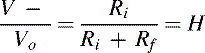
You will see that I have represented the forward or open-loop gain with the value G, and the feedback gain with the value H. (This diagram should look very familiar to those of you who have had training in control theory.) First, you see that the output is tied to the negative input. This is called negative feedback. What good is negative feedback? Let’s try an experiment. Hold your hand an inch over your desk, and keep it there. You are experiencing negative feedback right now. You are observing via sight and feel the distance from your hand to the desk. If your hand moves, you respond with a movement in the opposite direction. That is negative feedback. You invert the signal you receive via your senses and send it back to your arm. The same thing occurs when negative feedback is applied to an op-amp. The output signal is sent back to the negative input. A signal change in one direction at the output causes a Vsum to change in the opposite direction.
You should get an intuitive grasp of this negative feedback configuration. Look at the previous diagram and assume a value of 50,000 for G and a value of 1 for H. Now start by applying a 1 to the positive input. Assume the negative input is at 0 to begin with. That puts a value of 1 at the input of the gain block G and the output will start heading for the positive rail. But what happens as the output approaches 1? The negative input also approaches 1. The output of the summing block is getting smaller and smaller. If the negative input goes higher than 1, the input to the gain block G will go negative as well, forcing the output to go in the negative direction. Of course, that will cause a positive error to appear at the input of the gain block G, starting the whole process over again. Where will this all stop? It will stop when the negative input is equal to the positive input. In this case since H is 1, the output will be 1 also.
You have learned this in control theory. Look at the basic control equation in reference to the previous diagram:
![]() (19.3)
(19.3)
What happens when G is very large? The 1 in the denominator becomes insignificant and the equation becomes Vo = approximately Vi * (1 / H). H in this case is 1 so it follows that Vo = approximately Vi * (1 / 1) or,
![]() (19.4)
(19.4)
This is the special case where you can assume that the inputs of the op-amp are equal. Apply it ONLY when there is negative feedback. When feedback gain is one, this also demonstrates another neat op-amp circuit, the voltage follower. Whatever voltage is put on the positive input will appear at the output.
Take a look at the following figure. This is an op-amp in the negative feedback configuration. When you look at this, you should see a summer and an amplifier just as in the previous drawing. In this configuration, you can make the assumption that the positive and negative inputs are equal.
Negative feedback is the case that is drilled into you in school, and is the one that often causes confusion. It is a special case, a very widely used special case. Nonetheless, if you do not have negative feedback and the inputs and output are within operational limits, you must NOT assume the inputs of the op-amp are equal.
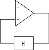
Figure 19.4 Original op-amp symbol with negative feedback
Why is this negative feedback configuration used so much? Remember the reason op-amps were invented? Amplifiers were tough to make. There had to be an easier way. Take a look at the control equation again:
![]() (19.5)
(19.5)
I have already shown that for large values of G, the equation approximates:
![]() (19.6)
(19.6)
You will see that the amplification of Vi depends on the value of H. For example, if we can make H equal 1/10, then Vo = Vi * (1 / (1 / 10)) or,
![]() (19.7)
(19.7)
How do we go about doing that? Do you remember the voltage divider circuit? That would be very useful here, as we would like H to be the equivalent of dividing by 10. Lets insert the voltage divider circuit in place of H. (Note, Vi will be connected to V+.)
Notice that the input to the voltage divider comes from the output of the op-amp, Vo. The output of the voltage divider goes to the negative input of the op-amp V−. Now, will the op-amp input V− affect the voltage divider circuit? NO! It has high impedance. It will not affect the divider. (If you didn’t get that, go back and read “what’s in an op-amp really” till you do!) Since the input to the divider is hooked to a voltage source,
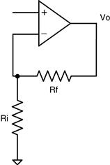
Figure 19.5 Negative feedback is a voltage divider
and the output is not affected by the circuit, we can calculate the gain from Vo to V– very easily with the voltage divider rule.
 (19.8)
Thus, it follows that:

or with a little algebra,
 (19.9)
There you have it—the gain of this op-amp circuit. Let’s look at it another way. Go back to the previous equation:
 (19.10)
We learned that in this special case of negative feedback we can assume that V+ = V–. This is because the negative feedback loop is pushing the output around, trying to reach this state. So let’s assume that Vi = V+ which is where the input to our amplifier will be hooked up. Now we can replace V– with Vi, and the equation looks like this:
 (19.11)
What we really want to know is what does the circuit do to Vi to get Vo? Let’s do a little math to come up with this equation:
 (19.12)
Please note that this is equal to 1/H. You see, the gain of this circuit is controlled by two simple resistors. Believe me, that is a whole lot easier to understand and calculate than a transistor amplification circuit. As you can see, the operation of this amplifier is pretty easy to understand.
Thumb Rules
• The negative feedback configuration is the only time you can assume that V− = V+.
• The high impedance inputs and the low impedance output make it easy to calculate the effects simple resistor networks can have in a feedback loop.
• The high open-loop gain of the op-amp is what makes the output gain of this special case equal to approximately 1/H.
• Op-amps were meant to make amplification easy, so don’t make it hard!
19.1.3 Positive Feedback
What is positive feedback? Let’s take a look at a real-world example. You are working one day, and your boss stops by and says, “Hey, you should know that you’ve handled your project very well, and that new op-amp circuit you built is awesome!” After you bask in his praise for a while, you find yourself working even harder than before. That is positive feedback. The output is sent back to the positive input, which in turn causes the output to move further in the same direction. Let’s look at the diagram of an op-amp again (Figure 19.6).
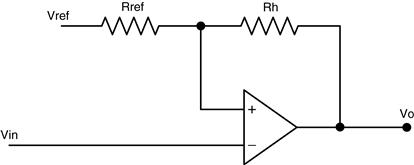
Figure 19.6 Positive feedback on an op-amp
Now we will do a little intuitive analysis. Don’t forget the thumb rules we learned in the last two sections. Review them now if you need to.
First, apply 0V to Vin. In this case the input is connected to V−. You also see that the output is connected via a resistor to a reference voltage, Vref. What is the voltage at V+? Does the voltage at V+ equal the voltage at V−? NO! (Don’t believe me? Check the thumb rules!)
What is the voltage at V+? That depends on two things: the voltage at Vref and the output voltage of the amplifier, Vo. Does the V+ input load the circuit at all? No, it does not. To begin the analysis, let Vref = 2.5V, and assume the output is equal to 0V. Now what is the voltage at V+? What do you know, since Vo is equal to 0, we have a basic voltage divider again. Assume Rref = 10K and Rh = 100K:
 (19.13)
So now there is 2.275V at V+ and 0V at V–. What will the op-amp do? Let’s refer to the block diagram of the op-amp we learned earlier (Figure 19.7).

Figure 19.7 Start with what is really inside!
What do we have? Vsum is equal to V+ − V− or, in this case, Vsum = 2.275V. Vo is equal to Vsum * G. The output will obviously go to the positive rail (if this is not obvious to you, you need to review, “What is an op-amp really?” again). Now we have Vo at the positive rail. Let’s assume that it is 4V for this particular op-amp. (Remember, the output rails depend on the op-amp used, and you should always refer to the datasheets for that information. 4V used in this case is typical for an LM324 with a 0 to 5V supply.)
The output is at 4V and V− is at 0V, but what about V+? It has changed. We must go back and analyze it again. (Do you feel like you are going in circles? You should. That is what feedback is all about; outputs affect inputs which affect the outputs, and so on, and so on.) The analysis this time has changed slightly. It is no longer possible to use just the voltage divider rule to calculate V+. We must also use superposition.
In superposition, you set one voltage source to 0 and analyze the results, and then you set the other source to 0 and analyze the results. Then you add the two results together to get the complete equation. Let’s do that now. We already know the result due to Vref from above. Here is the positive feedback diagram again for reference (Figure 19.8).
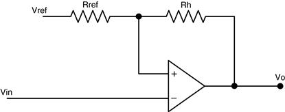
Figure 19.8 Positive feedback on an op-amp
Here is the result due to Vref using the voltage divider rule:
(19.14)
Here is the result due to Vo using the voltage divider rule:
 (19.15)
The result due to both is thus:
![]()
 (19.16)
Now insert all the current values and we have:
 (19.17)
Is this circuit stable now? Yes, it is. We have 0V at V–, and 2.64V at V+. This results in a positive error which, when amplified by the open-loop gain of the op-amp, causes the output to go to the positive rail. This is 4V, which is the state that we just analyzed.
Let’s change something. Let’s start slowly ramping up the voltage at V−. At what point will the op-amp output change? Right after the voltage at V− exceeds the voltage at V+. This results in a negative error, causing the output to swing to the negative rail. And what happens to V+? It changes back to 2.275V as we calculated above. So how do we get the output to go positive again? We adjust the input to less than 2.275V. The positive feedback reinforces the change in the output, making it necessary to move the input farther in the opposite direction to affect another change in the output.
The effect that I have just described is called hysteresis. It is an effect very commonly created using a positive feedback loop with an op-amp. What is hysteresis good for, you ask. Well, heating your house for one thing. It is hysteresis that keeps your furnace from clicking on and off every few seconds. Your oven and refrigerator use this principle as well. In fact, the disk drive on the computer I used to write this uses hysteresis to store information.
One important item to note. The size of the hysteresis window depends on the ratio of the two resistors Rref and Rh. In most typical applications Rh is much larger that Rref. If the signal at Vi is smaller than the window, it is possible to create a circuit that latches high or low and never changes. This is usually not desired and can be avoided be performing the analysis above and comparing the calculated limits to the input signal range.
Now that we have covered the three basic configurations of an op-amp, let’s put together a simple circuit that uses them. Here we have a voltage follower, hooked to a comparator using hysteresis, with an LED as an indicator (Figure 19.9).

Figure 19.9 Simple op-amp circuit for your bench to understand both positive and negative feedback
You should build this in your lab to gain an intuitive understanding of what has been discussed. Experiment with feedback changes in all parts of the circuit. Note that you can change the input potentiometers from 5K to 100K without affecting the voltage at which the comparator switches.
19.1.4 All About Op-Amps
There you have it, the basics of op-amp circuits. With this information, you can analyze most op-amp circuits you come across and build some really neat circuits yourself. What about filters, you say! Well, a filter is nothing more than an amplifier that changes gain depending on the frequency. Simply replace the resistors with an impedance and thus add a frequency component to the circuit. What about oscillators, you say? These are feedback circuits where timing of the signals is important. They still follow the rules above. I believe that grasping the basics of any discipline is the most important thing you can do. If you understand the basics, you can always build on that foundation to obtain higher knowledge, but if you do not “get the basics” you will flounder in your chosen field.
Thumb Rules
• Op-amp inputs are high impedance (that means no current flows into the inputs); this can’t be said too much so forgive me for repeating it.
• Op-amp outputs are low impedance.
• V+ = V− only if negative feedback is present, they don’t have to equal if feedback is positive.
• Positive feedback creates hysteresis when properly set up.
• Positive feedback can make an output latch to a state and stay there.
• Positive feedback with a delay can cause an oscillation.
• Op-amps were designed to make it easy, so don’t make it hard!
19.2 Understanding Op-Amp Parameters
This section is about op-amp data sheet parameters. The designer must have a clear understanding of what op-amp parameters mean and their impact on circuit design. The section is arranged for speedy access to parameter information. Their definitions, typical abbreviations, and units appear in Section 19.2.1. Section 19.2.2 Section 19.2.1. Section 19.2.2 digs deeper into important parameters for the designer needing more in-depth information.
While these parameters are the ones most commonly used at Texas Instruments, the same parameter may go by different names and abbreviations at other manufacturers. Not every parameter listed here may appear in the data sheet for a given op-amp. An op-amp that is intended only for AC applications may omit DC offset information. The omission of information is not an attempt to “hide” anything. It is merely an attempt to highlight the parameters of most interest to the designer who is using the part the way it was intended. There is no such thing as an ideal op-amp—or one that is universally applicable. The selection of any op-amp must be based on an understanding of what particular parameters are most important to the application.
If a particular parameter cannot be found in the data sheet, a review of the application may well be in order and another part, whose data sheet contains the pertinent information, might be more suitable. Texas Instruments manufactures a broad line of op-amps that can implement almost any application. The inexperienced designer could easily select an op-amp that is totally wrong for the application. Trying to use an audio op-amp with low total harmonic distortion in a high-speed video circuit, for example, will not work—no matter how superlative the audio performance might be.
Some parameters have a statistically normal distribution. The typical value published in the data sheet is the mean or average value of the distribution. The typical value listed is the 1σ value. This means that in 68% of the devices tested, the parameter is found to be ± the typical value or better. Texas Instruments currently uses 6σ to define minimum and maximum values. Usually, typical values are set when the part is characterized and never change.
19.2.1 Operational Amplifier Parameter Glossary
There are usually three main sections of electrical tables in op-amp data sheets. The absolute maximum ratings table and the recommended operating conditions table list constraints placed upon the circuit in which the part will be installed. Electrical characteristics tables detail device performance.
Absolute maximum ratings are those limits beyond which the life of individual devices may be impaired and are never to be exceeded in service or testing. Limits, by definition, are maximum ratings, so if double-ended limits are specified, the term will be defined as a range (e.g., operating temperature range).
Recommended operating conditions have a similarity to maximum ratings in that operation outside the stated limits could cause unsatisfactory performance. Recommended operating conditions, however, do not carry the implication of device damage if they are exceeded.
Electrical characteristics are measurable electrical properties of a device inherent in its design. They are used to predict the performance of the device as an element of an electrical circuit. The measurements that appear in the electrical characteristics tables are based on the device being operated within the recommended operating conditions.
Table 19.1 is a list of parameters and operating conditions that are commonly used in TI op-amp data sheets. The glossary is arranged alphabetically by parameter name. An abbreviation cross-reference is provided after the glossary in Table 19.2 to help the designer find information when only an abbreviation is given. More detail is given about important parameters in Section 19.2.2.
Table 19.1 Op-amp parameter glossary


Table 19.2 Cross-reference of op-amp parameters
| ABBV | Parameter |
| αIIO | Temperature coefficient of input offset current |
| ΔVCC±/ ΔVDD± | Supply voltage sensitivity |
| αVIO | Temperature coefficient of input offset voltage |
| ΔVIO | Supply voltage sensitivity |
| AD | Differential gain error |
| Am | Gain margin |
| AOL | Open-loop voltage gain |
| AV | Large-signal voltage amplification |
| AVD | Differential voltage amplification |
| B1 | Unity gain-bandwidth |
| BOM | Maximum-output-swing bandwidth |
| ci | Input capacitance |
| Cic | Common-mode input capacitance |
| CMRR | Common-mode rejection ratio |
| GBWP | Gain-bandwidth product |
| ICC-SHDN/IDD-SHDN | Supply current (shutdown) |
| ICC/IDD | Supply current |
| II | Input current |
| IIB | Input bias current |
| IIO | Input offset current |
| In | Input noise current |
| IO | Output current |
| IOL | Low-level output current |
| IOS | Short-circuit output current |
| kCMR | Common-mode rejection ratio |
| kSVR | Supply rejection ratio |
| kSVS | Supply voltage sensitivity |
| NF | Noise figure |
| PD | Total power dissipation |
| PSRR | Power supply rejection ratio |
| ri | Input resistance |
| Rid | Differential input resistance |
| Ro | Output resistance |
| Rt | Open-loop transresistance |
| SR | Slew rate |
| TA | Operating temperature |
| tDIS | Turn-off time (shutdown) |
| tEN | Turn-on time (shutdown) |
| THD | Total harmonic distortion |
| tf | Fall time |
| THD+N | Total harmonic distortion plus noise |
| tr | Rise time |
| ts | Settling time |
| TS | Storage temperature |
| VCC/VDD | Supply voltage |
| VI | Input voltage range |
| VIC | Common-mode input voltage |
| VICR | Input common-mode voltage range |
| VID | Differential input voltage |
| VIHSHDN | Turn-on voltage (shutdown) |
| VIL-SHDN | Turn-off voltage (shutdown) |
| VIO, VOS | Input offset voltage |
| Vn | Input noise voltage |
| VO(PP) | Maximum peak-to-peak output voltage swing |
| VOH | High-level output voltage |
| VOL | Low-level output voltage |
| VOM± | Maximum peak output voltage swing |
| XT | Crosstalk |
| Zic | Common-mode input impedance |
| Zo | Output impedance |
| Zt | Open-loop transimpedance |
| ΦD | Differential phase error |
| Φm | Phase margin |
19.2.2 Additional Parameter Information
Depending on the application, some op-amp parameters are more important than others. This section contains additional information for parameters that impact a broad range of designs.
19.2.2.1 Input Offset Voltage
All op-amps require a small voltage between their inverting and noninverting inputs to balance mismatches due to unavoidable process variations. The required voltage is known as the input offset voltage and is abbreviated VIO. VIO is normally modeled as a voltage source driving the noninverting input.
Figure 19.10 shows two typical methods for measuring input offset voltage—DUT stands for device under test. Test circuit (a) is simple, but since Vout is not at zero volts, it does not really meet the definition of the parameter. Test circuit (b) is referred to as a servo loop. The action of the loop is to maintain the output of the DUT at zero volts.

Figure 19.10 Test circuits for input offset voltage
Bipolar input op-amps typically offer better offset parameters than JFET or CMOS input op-amps.
TI data sheets show two other parameters related to VIO; the average temperature coefficient of input offset voltage, and the input offset voltage long-term drift.
The average temperature coefficient of input offset voltage, αVIO, specifies the expected input offset drift over temperature. Its units are μV/°C. VIO is measured at the temperature extremes of the part, and αVIO is computed as ΔVIO/Δ°C.
Normal aging in semiconductors causes changes in the characteristics of devices. The input offset voltage long-term drift specifies how VIO is expected to change with time. Its units are μV/month.
VIO is normally attributed to the input differential pair in a voltage feedback amplifier. Different processes provide certain advantages. Bipolar input stages tend to have lower offset voltages than CMOS or JFET input stages.
Input offset voltage is of concern anytime that DC accuracy is required of the circuit. One way to null the offset is to use external null inputs on a single op-amp package (Figure 19.11). A potentiometer is connected between the null inputs with the adjustable terminal connected to the negative supply through a series resistor. The input offset voltage is nulled by shorting the inputs and adjusting the potentiometer until the output is zero.
Figure 19.11 Offset voltage adjust
19.2.2.2 Input Current
The input circuitry of all op-amps requires a certain amount of bias current for proper operation. The input bias current, IIB, is computed as the average of the two inputs:
![]() (19.18)
(19.18)
CMOS and JFET inputs offer much lower input current than standard bipolar inputs. Figure 19.12 shows a typical test circuit for measuring input bias currents.

Figure 19.12 Test Circuit –IIB
The difference between the bias currents at the inverting and noninverting inputs is called the input offset current, IIO = IN − IP. Offset current is typically an order of magnitude less than bias current.
Input bias current is of concern when the source impedance is high. If the op-amp has high input bias current, it will load the source and a lower than expected voltage is seen. The best solution is to use an op-amp with either CMOS or JFET input. The source impedance can also be lowered by using a buffer stage to drive the op-amp that has high input bias current.
In the case of bipolar inputs, offset current can be nullified by matching the impedance seen at the inputs. In the case of CMOS or JFET inputs, the offset current is usually not an issue and matching the impedance is not necessary.
The average temperature coefficient of input offset current, αIIO, specifies the expected input offset drift over temperature. Its units are μA/°C. IIO is measured at the temperature extremes of the part, and αIIO is computed as ΔIIO/Δ°C.
19.2.2.3 Input Common Mode Voltage Range
The input common voltage is defined as the average voltage at the inverting and noninverting input pins. If the common mode voltage gets too high or too low, the inputs will shut down and proper operation ceases. The common mode input voltage range, VICR, specifies the range over which normal operation is guaranteed.
Different input structures allow for different input common-mode voltage ranges: The LM324 and LM358 use bipolar PNP inputs that have their collectors connected to the negative power rail. This allows the common-mode input voltage range to include the negative power rail.
The TL07X and TLE207X type BiFET op-amps use P-channel JFET inputs with the sources tied to the positive power rail via a bipolar current source. This allows the common-mode input voltage range to include the positive power rail.
TI LinCMOS op-amps use P-channel CMOS inputs with the substrate tied to the positive power rail. This allows the common-mode input voltage range to include the negative power rail.
Rail-to-rail input op-amps use complementary n- and p-type devices in the differential inputs. When the common-mode input voltage nears either rail, at least one of the differential inputs is still active, and the common-mode input voltage range includes both power rails.
The trends toward lower, and single-supply voltages make VICR of increasing concern.
Rail-to-rail input is required when a noninverting unity-gain amplifier is used and the input signal ranges between both power rails. An example of this is the input of an analog-to digital-converter in a low-voltage, single-supply system.
High-side sensing circuits require operation at the positive input rail.
19.2.2.4 Differential Input Voltage Range
Differential input voltage range is normally specified as an absolute maximum. Exceeding the differential input voltage range can lead to breakdown and part failure.
Some devices have protection built into them, and the current into the input needs to be limited. Normally, differential input mode voltage limit is not a design issue.
19.2.2.5 Maximum Output Voltage Swing
The maximum output voltage, VOM±, is defined as the maximum positive or negative peak output voltage that can be obtained without wave form clipping, when quiescent DC output voltage is zero. VOM± is limited by the output impedance of the amplifier, the saturation voltage of the output transistors, and the power supply voltages. This is shown pictorially in Figure 19.13.

Figure 19.13 VOM±
This emitter follower structure cannot drive the output voltage to either rail. Rail-to-rail output op-amps use a common emitter (bipolar) or common source (CMOS) output stage. With these structures, the output voltage swing is only limited by the saturation voltage (bipolar) or the on resistance (CMOS) of the output transistors, and the load being driven.
Because newer products are focused on single-supply operation, more recent data sheets from Texas Instruments use the terminology VOH and VOL to specify the maximum and minimum output voltage.
Maximum and minimum output voltage is usually a design issue when dynamic range is lost if the op-amp cannot drive to the rails. This is the case in single-supply systems where the op-amp is used to drive the input of an A-to-D converter, which is configured for full scale input voltage between ground and the positive rail.
19.2.2.6 Large Signal Differential Voltage Amplification
Large signal differential voltage amplification, AVD, is similar to the open-loop gain of the amplifier except open-loop is usually measured without any load. This parameter is usually measured with an output load. Figure 19.20 shows a typical graph of AVD vs. frequency. AVD is a design issue when precise gain is required. The gain equation of a noninverting amplifier:
(19.19)
β is a feedback factor, determined by the feedback resistors. The term ![]() in the equation is an error term. As long as AVD is large in comparison with
in the equation is an error term. As long as AVD is large in comparison with ![]() it will not greatly affect the gain of the circuit.
it will not greatly affect the gain of the circuit.
19.2.2.7 Input Parasitic Elements
Both inputs have parasitic impedance associated with them. Figure 19.14 shows a model of the resistance and capacitance between each input terminal and ground and between the two terminals. There is also parasitic inductance, but the effects are negligible at low frequency.

Figure 19.14 Input parasitic elements
Input impedance is a design issue when the source impedance is high. The input loads the source.
Input Capacitance
Input capacitance, Ci, is measured between the input terminals with either input grounded. Ci is usually a few pF. In Figure 19.14, if Vp is grounded, then Ci = Cd || Cn.
Sometimes common-mode input capacitance, Cic is specified. In Figure 19.14, if Vp is shorted to Vn, then Cic = Cp || Cn ⋅ Cic is the input capacitance a common mode source would see referenced to ground.
Input Resistance
Input resistance, ri is the resistance between the input terminals with either input grounded.
In Figure 19.14, if Vp is grounded, then ri = Rd || Rn. ri ranges from 107Ω to 1012Ω, depending on the type of input.
Sometimes common-mode input resistance, ric, is specified. In Figure 19.14, if Vp is shorted to Vn, then ric = Rp || Rn ⋅ ric is the input resistance a common mode source would see referenced to ground.
19.2.2.8 Output Impedance
Different data sheets list the output impedance under two different conditions. Some data sheets list closed-loop output impedance while others list open-loop output impedance, both designated by Zo.
Zo is defined as the small signal impedance between the output terminal and ground. Data sheet values run from 50Ω to 200Ω.
Common emitter (bipolar) and common source (CMOS) output stages used in rail-to-rail output op-amps have higher output impedance than emitter follower output stages.
Output impedance is a design issue when using rail-to-rail output op-amps to drive heavy loads. If the load is mainly resistive, the output impedance will limit how close to the rails the output can go. If the load is capacitive, the extra phase shift will erode phase margin.
Figure 19.15 shows how output impedance affects the output signal assuming Zo is mostly resistive.

Figure 19.15 Effect of output impedance
Some new audio op-amps are designed to drive the load of a speaker or headphone directly. They can be an economical method of obtaining very low output impedance.
19.2.2.9 Common-Mode Rejection Ratio
Common-mode rejection ratio, CMRR, is defined as the ratio of the differential voltage amplification to the common-mode voltage amplification, ADIF/ACOM. Ideally this ratio would be infinite with common mode voltages being totally rejected.
The common-mode input voltage affects the bias point of the input differential pair. Because of the inherent mismatches in the input circuitry, changing the bias point changes the offset voltage, which, in turn, changes the output voltage. The real mechanism at work is ΔVOS/ΔVCOM.
In a Texas Instruments data sheet, CMRR = ΔVCOM/ΔVOS, which gives a positive number in dB. CMRR, as published in the data sheet, is a DC parameter. CMRR, when graphed vs. frequency, falls off as the frequency increases.
A common source of common-mode interference voltage is 50-Hz or 60-Hz AC noise. Care must be used to ensure that the CMRR of the op-amp is not degraded by other circuit components. High values of resistance make the circuit vulnerable to common mode (and other) noise pick up. It is usually possible to scale resistors down and capacitors up to preserve circuit response.
19.2.2.10 Supply Voltage Rejection Ratio
Supply voltage rejection ratio, kSVR (a.k.a. power supply rejection ratio, PSRR), is the ratio of power supply voltage change to output voltage change.
The power voltage affects the bias point of the input differential pair. Because of the inherent mismatches in the input circuitry, changing the bias point changes the offset voltage, which, in turn, changes the output voltage.
For a dual supply op-amp, ![]() . The term ΔVCC± means that the plus and minus power supplies are changed symmetrically. For a single-supply op-amp,
. The term ΔVCC± means that the plus and minus power supplies are changed symmetrically. For a single-supply op-amp, ![]()
Also note that the mechanism that produces kSVR is the same as for CMRR. Therefore kSVR as published in the data sheet is a DC parameter like CMRR. When kSVR is graphed vs. frequency, it falls off as the frequency increases.
Switching power supplies produce noise frequencies from 50 kHz to 500 kHz and higher. kSVR is almost zero at these frequencies so that noise on the power supply results in noise on the output of the op-amp. Proper bypassing techniques must be used to control high-frequency noise on the power lines.
19.2.2.11 Supply Current
Supply current, IDD, is the quiescent current draw of the op-amp(s) with no load. In a Texas Instruments data sheet, this parameter is usually the total quiescent current draw for the whole package. There are exceptions, however, such as data sheets that cover single and multiple packaged op-amps of the same type. In these cases, IDD is the quiescent current draw for each amplifier.
In op-amps, power consumption is traded for noise and speed.
19.2.2.12 Slew Rate at Unity Gain
Slew rate, SR, is the rate of change in the output voltage caused by a step input. Its units are V/μs or V/ms. Figure 19.16 shows slew rate graphically. The primary factor controlling slew rate in most amps is an internal compensation capacitor CC, which is added to make the op-amp unity-gain stable. Referring to Figure 19.17, voltage change in the second stage is limited by the charging and discharging of the compensation capacitor CC. The maximum rate of change is when either side of the differential pair is conducting 2IE. Essentially SR = 2IE/CC. Remember, however, that not all op-amps have compensation capacitors. In op-amps without internal compensation capacitors, the slew rate is determined by internal op-amp parasitic capacitances. Noncompensated op-amps have greater bandwidth and slew rate, but the designer must ensure the stability of the circuit by other means.

Figure 19.16 Slew rate

Figure 19.17 Simplified op-amp schematic
In op-amps, power consumption is traded for noise and speed. In order to increase slew rate, the bias currents within the op-amp are increased.
19.2.2.13 Equivalent Input Noise
All op-amps have parasitic internal noise sources. Noise is measured at the output of an op-amp, and referenced back to the input. Therefore, it is called equivalent input noise.
Equivalent input noise parameters are usually specified as voltage, Vn, (or current, In) per root hertz. For audio frequency op-amps, a graph is usually included to show the noise over the audio band.
Spot Noise
The spectral density of noise in op-amps has a pink and a white noise component. Pink noise is inversely proportional to frequency and is usually only significant at low frequencies. White noise is spectrally flat. Figure 19.18 shows a typical graph of op-amp equivalent input noise.

Figure 19.18 Typical op-amp input noise spectrum
Usually spot noise is specified at two frequencies. The first frequency is usually 10 Hz where the noise exhibits a 1/f spectral density. The second frequency is typically 1 kHz where the noise is spectrally flat. The units used are normally ![]() or
or ![]() for current noise). In Figure 19.18 the transition between 1/f and white is denoted as the corner frequency, fnc.
for current noise). In Figure 19.18 the transition between 1/f and white is denoted as the corner frequency, fnc.
Broadband Noise
A noise parameter like VN(PP), is the a peak to peak voltage over a specific frequency band, typically 0.1 Hz to 1 Hz, or 0.1 Hz to 10 Hz. The units of measurement are typically nV P-P.
Given the same structure within an op-amp, increasing bias currents lowers noise (and increases SR, GBW, and power dissipation).
Also the resistance seen at the input to an op-amp adds noise. Balancing the input resistance on the noninverting input to that seen at the inverting input, while helping with offsets due to input bias current, adds noise to the circuit.
19.2.2.14 Total Harmonic Distortion Plus Noise
Total harmonic distortion plus noise, THD + N, compares the frequency content of the output signal to the frequency content of the input. Ideally, if the input signal is a pure sine wave, the output signal is a pure sine wave. Due to nonlinearity and noise sources within the op-amp, the output is never pure.
THD + N is the ratio of all other frequency components to the fundamental and is usually specified as a percentage:
 (19.20)
Figure 19.19 shows a hypothetical graph where THD + N = 1%. The fundamental is the same frequency as the input signal. Nonlinear behavior of the op-amp results in harmonics of the fundamental being produced in the output. The noise in the output is mainly due to the input noise of the op-amp. All the harmonics and noise added together make up 1% of the fundamental.

Figure 19.19 Output spectrum with THD + N = 1%
Two major reasons for distortion in an op-amp are the limit on output voltage swing and slew rate. Typically an op-amp must be operated at or below its recommended operating conditions to realize low THD.
19.2.2.15 Unity gain-bandwidth and phase margin
There are five parameters relating to the frequency characteristics of the op-amp that are likely to be encountered in Texas Instruments data sheets. These are unity-gain bandwidth (B1), gain-bandwidth product (GBWP), phase margin at unity-gain (ϕm), gain margin (Am), and maximum output-swing bandwidth (BOM).
Unity-gain bandwidth (B1) and gain-bandwidth product (GBWP) are very similar. B1 specifies the frequency at which AVD of the op-amp is 1:
![]() (19.21)
(19.21)
GBW specifies the gain-bandwidth product of the op-amp in an open-loop configuration and the output loaded:
![]() (19.22)
(19.22)
GBW is constant for voltage-feedback amplifiers. It does not have much meaning for current-feedback amplifiers because there is not a linear relationship between gain and bandwidth.
Phase margin at unity-gain (ϕm) is the difference between the amount of phase shift a signal experiences through the op-amp at unity-gain and 180°:
![]() (19.23)
(19.23)
Gain margin is the difference between unity-gain and the gain at 180° phase shift:
![]() (19.24)
(19.24)
Maximum output-swing bandwidth (BOM) specifies the bandwidth over which the output is above a specified value:
![]() (19.25)
(19.25)
The limiting factor for BOM is slew rate. As the frequency gets higher and higher the output becomes slew rate limited and can not respond quickly enough to maintain the specified output voltage swing.
In order to make the op-amp stable, capacitor, CC, is purposely fabricated on chip in the second stage (Figure 19.17). This type of frequency compensation is termed dominant pole compensation. The idea is to cause the open-loop gain of the op-amp to roll off to unity before the output phase shifts by 180°. Remember that Figure 19.17 is very simplified, and there are other frequency shaping elements within a real op-amp.
Figure 19.20 shows a typical gain vs. frequency plot for an internally compensated op-amp as normally presented in a Texas Instruments data sheet.

Figure 19.20 Voltage amplification and phase shift vs. frequency
As noted earlier, AVD falls off with frequency. AVD (and thus, B1 or GBW) is a design issue when precise gain is required of a specific frequency band.
Phase margin (ϕm) and gain margin (Am) are different ways of specifying the stability of the circuit. Since rail-to-rail output op-amps have higher output impedance, a significant phase shift is seen when driving capacitive loads. This extra phase shift erodes the phase margin, and for this reason most CMOS op-amps with rail-to-rail outputs have limited ability to drive capacitive loads.
19.2.2.16 Settling Time
It takes a finite time for a signal to propagate through the internal circuitry of an op-amp. Therefore, it takes a period of time for the output to react to a step change in the input. In addition, the output normally overshoots the target value, experiences damped oscillation, and settles to a final value. Settling time, ts, is the time required for the output voltage to settle to within a specified percentage of the final value given a step input.
Figure 19.21 shows this graphically:Settling time is a design issue in data acquisition circuits when signals are changing rapidly. An example is when using an op-amp following a multiplexer to buffer the input to an A-to-D converter. Step changes can occur at the input to the op-amp when the multiplexer changes channels. The output of the op-amp must settle to within a certain tolerance before the A-to-D converter samples the signal.

Figure 19.21 Settling time
19.3 Modeling Op-Amps
Virtually every op-amp supplier provides Spice models, which are a very useful approximation of device performance. There are two opposing criteria for such a model. It should use the fewest internal elements to ease computing, but it should also give an accurate representation of the device as a “black box.” You can use these models as a necessary (but not entirely sufficient) step in the design process. Models cannot capture a device’s every sensitivity to supply variations or temperature and load changes. Dynamic performance such as slew rate and overshoot are especially difficult to model, and peculiarities such as behavior at or beyond the common mode limits will be entirely absent.
The circuit design must be characterized for the entire range of performance characteristics that an off-the-shelf part might show, but generally available Spice models use typical rather than worst-case specs.
Even a perfect model would not capture what is just as critical in high-performance analog design: your physical circuit that surrounds the part. Just a few picofarads of circuit-board capacitance will change the frequency response, for example. Common impedances in the power or ground circuits can affect stability and power supply rejection. Conductive residues on the circuit provide a leakage path between IC pins. No model of itself will detail your circuit layout strays or ground topology.
This doesn’t mean you shouldn’t use models. Use them for initial assessments of your circuit, to about ±20% accuracy. At the same time, recognize that the model itself is neither perfect nor does it include the subtleties of your design. Check with the supplier to understand which modeled parameters are typical, which are worst-case, which are at room temperature, and other similar limitations and simplifications. The typically short development timescale, and the project manager champing at the bit, may constrain your ability to experiment and tempt you to go straight from the model to the final layout. But if there is any critical performance issue which you know is not covered by the model, be prepared for a few design iterations, and don’t be afraid to breadboard the design if possible.
Most suppliers offer evaluation boards and suggested circuit-board layout drawings, especially for high-performance or complex parts. An evaluation board shows you what the part can do in a reference design. The layout can serve as a starting point for your own implementation, so you won’t waste time discovering mistakes the application engineers have already made and dealt with. The first question an applications support engineer asks when a designer calls with a problem such as oscillation in high-frequency current-feedback circuits is, “Did you use the evaluation board layout?”
19.4 Finding the Perfect Op-Amp
The operational amplifier’s operation and circuits are easy to find in the books in your local university library. The amplifier operation and circuit descriptions found in these reference books take you through computational algorithms that theoretically will provide the solutions to your analog amplifier design woes. If there were a perfect amplifier on the market today, the designs found in these books would indeed be easy to implement successfully. But there isn’t a perfect amplifier—yet. Throughout the history of analog system design, circuits have required special care in key areas in order to ensure success. As luck would have it, a little common sense and bench sense will pull you out of most of your amplifier design disasters.
In an ideal world, the perfect amplifier would look like the one described in Figure 19.22.
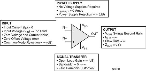
Figure 19.22 A perfect amplifier has an infinite input impedance, open-loop gain, power supply rejection ratio, common-mode rejection ratio, bandwidth, slew rate and output current. It also has zero offset voltage, input noise, output impedance, power dissipation and most importantly, zero cost.
The input stage design of this perfect amplifier would use devices whose inputs (IN+ and IN−) extend all the way to the power supply rails. Some single-supply amplifiers are able to do this with some distortion, but the perfect amplifier would be distortion-free. As a matter of fact, it would be nice if the inputs operated beyond the rails. If this were the case, the common-mode range goes beyond the rails as well.
Additionally, the inputs would not source or sink current—that is, they would have zero-input bias current. This allows source impedances to the amplifier to be infinite. This implies no common-mode or differential-mode input capacitance. Since voltage errors across the two inputs are usually gained by closed-loop circuit configurations around the amplifier, any DC voltage error (offset voltage) or AC error (noise) would be zero. The absence of these errors removes all of your calibration worries!
As for the power supply requirements of this ideal amplifier, there would be none. As you know, industry trends are always working on requests for lower supply voltages, and consequently, lower power consumption from active components. The ideal amplifier wouldn’t need a voltage supply across VDD and VSS and would have zero power dissipation in its quiescent state.
The output of this amplifier would be capable of really swinging rail-to-rail, or even beyond. This would eliminate the problem of losing bits on the outer rim in the following A/D conversion. The output impedance would be zero at DC, as well as over frequency ensuring that the device connected to the input of the amplifier is perfectly isolated from the external output device. The op-amp would respond to input signals instantaneously—that is, the slew rate would be infinite and it would be able to drive any load (resistive or capacitive) while maintaining an infinite open-loop gain and rail-to-rail output swing performance. Finally, in the frequency domain, the open-loop gain would be infinite at DC as well as over frequency, and the bandwidth of the amplifier would also be infinite. Oh, did I forget price? We would all love to have this ideal amplifier for $0.00.
Welcome to op-amp 101! This describes the textbook amplifier.
I know that if I’m able to figure out how to design this amplifier, I guarantee you, I will become a multizillionaire. At this point, you are probably saying, “Only in your dreams!” Well, maybe not a multizillionaire, mainly because the profits are $0.00. However, it is certain that I will become a very popular (still poor) person.
It is interesting to note that many of these design imperfections are used to an advantage by most designers. For example, an amplifier circuit design uses a less than infinite bandwidth to limit the noise and high-speed transients in circuits. An infinite slew rate is not as good as it sounds. The amplifier users enjoy slower signals. This reduces the glitches further down the signal path and simplifies the layout.
So, for today, we know that there isn’t an ideal amplifier for all circuit situations. The best we can do with the choices available is to pick the best amplifier for our application circuit and then use it properly.
19.4.1 Choose the Technology Wisely
CMOS and bipolar are the two silicon technologies that single-supply operational amplifiers commonly use. Figure 19.23 shows the differences between these two operational amplifier technologies. The most important difference between CMOS and bipolar is in the input stage transistors. These transistors have a profound effect on the overall operation of the amplifier.

Figure 19.23 The two silicon technologies that single-supply amplifiers are manufactured with are CMOS or bipolar processes. By using the CMOS process, you can manufacture bipolar amplifiers. In these designs, the input transistors are bipolar, and the remaining transistors are CMOS.
Because of the difference between the input transistors of these two types of amplifiers, the CMOS amplifier has lower input current noise and higher input impedance. Because of the high input impedance, the input bias current of the CMOS amplifier is much lower. In fact, the electrostatic discharge (ESD) cells at the input of the CMOS amplifier cause the input bias current errors. As will be shown in circuits later in this chapter, we can use this to an advantage for high impedance sources, such as photosensing transimpedance amplifiers.
The CMOS amplifier typically has a higher open-loop gain than bipolar amplifiers. This can minimize gain error in applications where the closed-loop gain is extremely high (60 dB or greater).
In contrast with the CMOS amplifier, the bipolar amplifier usually has lower input-voltage noise, room temperature offset-voltage and offset-drift. Bipolar amplifiers are more likely to provide higher output drive. They also exhibit a higher common-mode rejection capability. This is useful if the amplifier is in a buffer configuration. Although these specifications are typically better than the CMOS amplifier counterpart, the input bias current and input current noise is considerably higher.
Single-supply operating conditions are perfect for both CMOS and bipolar amplifiers. With the proper IC design, they are also capable of input and (near) output rail-to-rail operation.
19.4.2 Fundamental Operational Amplifier Circuits
The op-amp is the analog building block that is analogous to the digital gate. By using the op-amp in the design, circuits can be configured to modify the signal in the same fundamental way that the inverter, AND and OR gates do in digital circuits. This section of the chapter will show the fundamental circuits using this building block. The list of circuits we will discuss include the voltage follower, noninverting gain and inverting gain circuits. This will be followed by more complex circuits, including a difference amplifier, summing-amplifier and current-to-voltage converter.
19.4.2.1 Voltage Follower Amplifier
Starting with the most basic op-amp circuit, the buffer amplifier (shown in Figure 19.24) is used to drive heavy loads, solve impedance matching problems, or isolate high power circuits from sensitive, precise circuitry. Usually, heavy loads require an additional specialized amplifier that is capable of supplying the higher output currents that are greater than 20 mA. You will find that the amplifier data sheet has specifications for the magnitude of the amplifier output current, capable of driving higher currents.
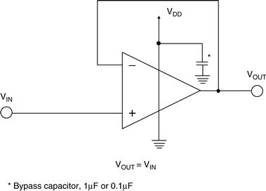
Figure 19.24 A buffer amplifier, also called a voltage follower, is useful when you want to provide a high-current drive stage, match impedances or electrically isolate signals.
Solving impedance matching problems is also a good reason to use a buffer amplifier. This type of problem exists when the signal path has a high impedance device or resistor that creates an undesirable voltage divider in the circuit. A buffer amplifier breaks up this type of impedance path because of the high impedance input and low impedance output of the amplifier.
Another use for a buffer is to keep high thermal changes away from sensitive circuits. In this scenario the buffer follows the sensitive circuit and serves the purpose of driving high output currents.
The buffer amplifier as shown in Figure 19.24 can be implemented with any single-supply, unity-gain stable amplifier. In this circuit, as with all amplifier circuits, bypassing the op-amp power with a capacitor is a must. For single-supply amplifiers that operate in bandwidths from DC to 1 MHz, a 1 μF capacitor is usually appropriate. Sometimes a smaller bypass capacitor is required for amplifiers that have bandwidths of up to the tens to hundreds of megahertz. In these cases, a 0.1 μF capacitor would be appropriate. If the selection of the value of the bypass capacitor is an inappropriate value or placed too far from the power supply pin and not connected to ground directly on the PCB, the op-amp circuit may oscillate. If you are unsure of what the bypass capacitor value should be, refer to the product data sheet for details.
The analog gain of the circuit in Figure 19.24 is +1 V/V. Notice that this circuit has positive overall gain, but the feedback loop is tied from the output of the amplifier to the inverting input. An all too common error is to assume that an op-amp circuit that has a positive gain requires positive feedback. You can configure this amplifier with positive feedback if you connect the noninverting input to the output. I know this sounds unbelievable, but I have had applicants draw buffers with positive feedback during their interviews. If positive feedback is used, the amplifier will most likely drive to either rail at the output.
This amplifier circuit will give good linear performance across the bandwidth of the amplifier. And, you may be looking at this discussion and saying to yourself, “There is that textbook description, again.” You are right; however, here are the land mines in this type of circuit.
The only restrictions on the signal will occur as a result of a violation of the input common-mode voltage and output swing limits. You need to scrutinize these performance characteristics in your amplifier data sheet and your application’s demands on this type of circuit. Oh, by the way, ensure that the bandwidth of the amplifier is at least 100× higher than the bandwidth of your signal. However, be aware that you need to look at the input and output of the amplifier.
When using this circuit to drive heavy loads, the specifications of the amplifier must indicate that it is capable of providing the required output currents. Another application where this circuit may be used is to drive capacitive loads. Not every amplifier is capable of driving capacitors without becoming unstable. If an amplifier can drive capacitive loads, the product data sheet will highlight this feature. However, if an amplifier can’t drive capacitive loads, the product data sheets will not explicitly say so. This is an instance where features are not in the advertisements or promotions and there is no mention of average performance.
Another use for the buffer amplifier is to solve impedance-matching problems. This would be applicable in a circuit where the analog signal source has relatively high impedance as compared to the impedance of the following circuitry. If this occurs, there will be a voltage loss with the signal because of the voltage divider between the source’s impedance and the following circuitry’s impedance. The buffer amplifier is a perfect solution to the problem. The input impedance of the noninverting input of an amplifier can be as high as 1013Ω for CMOS amplifiers. In addition, the output impedance of this amplifier configuration is usually less than 100Ω.
Yet another use of this configuration is to separate a heat source from sensitive precision circuitry, as shown in Figure 19.25. Imagine that the input circuitry to this buffer amplifier is amplifying a 100 mV signal. This type of amplification is difficult to do with any level of accuracy in the best of situations. Assigning the output current drive to the device that is doing the precision, amplification work can easily disrupt this measurement. An increase in current drive will cause self-heating of the chip, which will induce an offset change. In this circuit (Figure 19.25), the front-end circuitry makes precision measurements, while an analog buffer performs the function of driving a heavy load.

Figure 19.25 A buffer amplifier helps achieve load isolation in this circuit. The buffer separates any high-current output requirements from this input amplifier.
19.4.2.2 Amplifying Analog Signals
The buffer solves many analog signal problems; however, there are instances in circuits where you need to gain a signal. Two fundamental types of amplifier circuits can provide gain. With the first type, the signal gain is positive (or not inverted) as shown in Figure 19.26. This type of circuit is useful in single-supply amplifier applications where negative voltages are usually not present, difficult to produce or just not possible.

Figure 19.26 This is an operational amplifier configured in a noninverting gain circuit. This circuit applies a positive gain to a signal in your circuit. Therefore, you won’t need a reference level-shift voltage to keep the output of the amplifier within its operating range.
The input signal to this circuit is presented to the high impedance, noninverting input of the op-amp. The gain that the amplifier circuit applies to the signal is equal to:
![]() (19.26)
(19.26)
Typical values for these resistors in single-supply circuits are above 5 kΩ to 25 kΩ for R2. For the input resistor, R1, restrictions are dependent on the amount of gain desired versus the amount of amplifier noise and input offset voltage as specified in the product data sheet of the op-amp.
Again, this circuit has some restrictions in terms of the input and output range. The common-mode range of the amplifier restricts the noninverting input. The output swing of the amplifier is also restricted as stated in the product data sheet of the individual amplifier. Most typically, the larger signal at the output of the amplifier causes more signal-clipping errors than the smaller signal at the input. Reducing the gain of this circuit may eliminate undesirable output clipping errors.
Figure 19.27 illustrates an inverting amplifier configuration. This circuit gains and inverts the signal present at the input resistor, R1. The gain equation for this circuit is:
![]() (19.27)
(19.27)
The ranges for R1 and R2 are the same as in the noninverting circuit shown in Figure 19.26.

Figure 19.27 This is an operational amplifier configured in an inverting gain circuit. Single-supply environments usually require VBIAS to ensure the output stays above ground.
This circuit has a minor pitfall in single-supply circuits. In single-supply applications, this circuit is easy to misuse. The problem is rooted in the selection of the voltage at VBIAS. You need to select a value for VBIAS so that the output of the amplifier always remains between the supplies.
For example, let R2 equal 10 kΩ, R1 equal 1 kΩ, VBIAS equal 0V, and the voltage at the input resistor, R1, equal to 100 mV, the output voltage would be −1V. This would violate the output swing range of the operational amplifier. In reality, the output of the amplifier would try to go as near to ground as possible.
The inclusion of a positive DC voltage at VBIAS in this circuit solves this problem. In the previous example, a voltage of 225 mV applied to VBIAS would level shift the output signal up 2.475V. This would make the output signal equal (2.475V − 1V) or 1.475V at the output of the amplifier. Typically, you want to make the target average output voltage of the amplifier equal to VDD/2.
19.4.2.3 The Difference Amplifier
The difference amplifier combines the noninverting amplifier and inverting amplifier circuits of Figure 19.26 and Figure 19.27 into a signal block that subtracts two signals. Figure 19.28 illustrates an example of the difference amplifier circuit.

Figure 19.28 This is an operational amplifier circuit configured in a difference amplifier circuit. A difference amplifier implements the subtraction and gain function in one stage.
Figure 19.28 illustrates a straightforward implementation of this function. A difference amplifier or op-amp subtractor uses this arrangement of resistors around an amplifier. The DC transfer function of this circuit is equal to:
 (19.28)
If R1/R2 is equal to R3/R4, the closed loop system gain of this circuit equals:
![]() (19.29)
(19.29)
This circuit configuration will reliably take the difference of two signals as long as the signal-source impedances are low. If the signal source impedances are high with respect to R1, there will be a signal loss due to the voltage divider action between the source and the input resistors to the difference amplifier. Additionally, errors can occur if the two signal source impedances are mismatched. With this circuit, it is possible to have gains equal to or higher than one.
The fact that R1/R2 is equal to R3/R4 simplifies the mathematics in this system considerably. Since the gain of both signals is equal, the difference amplifier conveniently subtracts the common-mode voltage of the two signals from the system. It is also easy to implement gain by setting the two resistor ratios to be equal or greater than one.
One limitation of this circuit is the lack of flexibility with gain adjustments. If you change the gain dynamically in the application, you must adjust two resistors. In a single-supply environment, a voltage reference centers the output signal between ground and the power supply. Figure 19.28 shows this voltage, “VSHIFT.” The purpose of this reference voltage is to simply shift the output signal into the linear region of the amplifier. A precision, voltage-reference, or a resistive network implements the VSHIFT circuit function as shown in Figure 19.29.
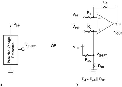
Figure 19.29 A precision voltage reference, (a) or a less expensive solution of replacing R4 of the voltage divider between the supply, (b) provides the voltage, VSHIFT, of this difference amplifier.
19.4.2.4 Summing Amplifier
You can use summing amplifiers to combine multiple signals by addition or subtraction. Since the difference amplifier can only process two signals, it is a subset of the summing amplifier.
The transfer function of this circuit as shown in Figure 19.30 is:
![]() (19.30)
(19.30)
You can use any number of inputs on either the inverting or noninverting input sides as long as there are an equal number of both with equivalent resistors. All of the inputs to this circuit should be connected to a signal source or (if unused) to the ground.
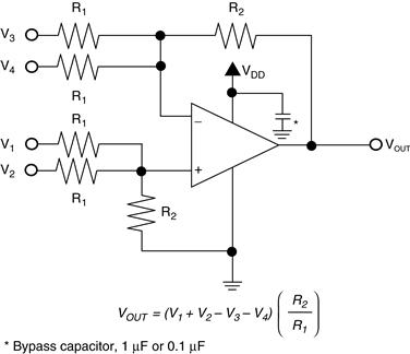
Figure 19.30 Operational amplifier configured in a summing amplifier circuit.
19.4.2.5 Current-to-Voltage Conversion
If you use a photodetector, feedback resistor and an operational amplifier in your circuit you can sense light. This type of circuit converts the output current of a photodetector into a voltage. The single resistor and an optional capacitor are in the feedback-loop of the amplifier as shown in Figure 19.31.

Figure 19.31 These circuits show how to convert current to voltage by using an amplifier and one resistor. The top light-sensing circuit is appropriate for precision applications. The bottom circuit is appropriate for high-speed applications.
In the circuits shown in Figure 19.31, light impinging on the photodetector generates a current. This current flows in the reverse bias direction of the diode. If a CMOS op-amp is used (with low input bias current), the current from the detector (ID1) primarily goes through the feedback resistor, R2. Additionally, the op-amp input bias current error is low because it is CMOS (typically <200 pA). You would ground the noninverting input of the op-amp, which keeps the entire circuit biased to ground. These two circuits will only work if the common mode range of the amplifier includes zero and you are not concerned about a zero level of light. If your light source has zero luminance, the output of the single-supply amplifier is unable to go all the way to ground.
The two circuits in Figure 19.31 provide precision-sensing from the photodetector (top circuit in the figure) and higher speed sensing (bottom circuit in the figure). In the top circuit, the voltage across the detector is nearly zero and equal to the offset voltage of the amplifier. With this configuration, current that appears across the resistor, R2, is primarily a result of the light excitation on the photodetector.
The photosensing circuit at the bottom of the figure works best in a high-speed, digital environment. By reverse biasing the photodetector (which reduces the parasitic capacitance of the diode), this sensing circuit can respond very quickly to digital signals. There is more leakage through the photodetector in this bottom circuit, which causes a higher DC error.
19.4.3 Using these Fundamentals
You can use several amplifiers to build instrumentation amplifiers and floating current sources.
19.4.3.1 Instrumentation Amplifier
You will find instrumentation amplifiers in a large variety of applications from medical instrumentation to process control. The instrumentation amplifier is similar to the difference amplifier in that it subtracts one analog signal from another, but it differs in terms of the quality of the input stage. Figure 19.32 illustrates a classic, three op-amp instrumentation amplifier.

Figure 19.32 You can design an instrumentation amplifier with three amplifiers. The input operational amplifiers (A1, A2) provide signal gain. The output operational amplifier converts the signal from the two input amplifiers to a single-ended output with a difference amplifier (A3).
In this circuit, the high impedance, noninverting inputs of the input amplifiers (A1, A2) acquire the two input signals. This is a distinct advantage over the difference amplifier configuration where source impedances are high or mismatched. The first stage also gains the two incoming signals. One resistor, RG, adjusts the gain.
Following the first stage of this circuit is a difference amplifier (A3). The function of this portion of the circuit is to reject the common-mode voltage of the two input signals as well as take the difference between them. The source impedances of the signals into the input of the difference amplifier are low, equivalent and well controlled.
The reference voltage (VREF) of the difference stage of this instrumentation amplifier is capable of spanning a wide range. Typically, you would connect the voltage reference to half of the supply voltage in a single-supply application. The transfer function of this circuit is:
![]() (19.31)
(19.31)
Figure 19.33 shows a second type of instrumentation amplifier. In this circuit, the two amplifiers serve the functions of load isolation and signal gain. The second amplifier also takes the difference between the two input signals (V1, V2).

Figure 19.33 You can design an instrumentation amplifier with two amplifiers. This configuration is best suited for higher gains (gain ≥ 3 V/V).
You would connect the circuit reference voltage to the first op-amp in the signal chain. Typically, this voltage is half of the supply voltage in a single-supply environment.
The transfer function of this circuit is:
![]() (19.32)
(19.32)
19.4.3.2 Floating Current Source
A floating current source (Figure 19.34) can come in handy when driving a variable resistance, like a resistance temperature device (RTD). This particular configuration produces an appropriate 1 mA source for an RTD-type sensor. However, you can change this current reference magnitude to any current.

Figure 19.34 A floating current source uses two operational amplifiers and a precision voltage reference.
With this configuration, R1 reduces the voltage of VREF by the voltage VR1. The voltage applied to the noninverting input of the top op-amp is VREF − VR1. This voltage is gained to the amplifier’s output by two, to equal 2 × (VREF − VR1). Meanwhile, the output for the bottom op-amp (A2) is presented with the voltage VREF − 2 VR1. Subtracting the voltage at the output of the top-amplifier from the noninverting input of the bottom amplifier gives 2 × (VREF − VR1) − (VREF − 2 VR1), which equals VREF.
The transfer function of the circuit is:
![]() (19.33)
(19.33)
19.4.4 Amplifier Design Pitfalls
Theoretically, the circuits within this chapter work. Beyond the theory, however, there are a few tips that will help get the circuit right the first time. This section lists common problems associated with using an op-amp on a PC board. The following discussion has two categories: general suggestions and single-supply pitfalls.
19.4.4.1 In General
• Be careful of the supply pins. Don’t make them too high per the amplifier specification sheet and don’t make them too low. High supplies will damage the part. In contrast, low supplies won’t bias the internal transistors and the amplifier won’t work or it may not operate properly.
• Make sure the negative supply is, in fact, tied to a low impedance potential. Additionally, make sure the positive supply is the voltage you expect with respect to the negative supply pin of the op-amp. Placing a voltmeter across the negative and positive supply pins will verify that you have the right relationship between the pins.
• Ground can’t be trusted, especially in digital circuits. Plan your grounding scheme carefully. If the circuit has a lot of digital circuitry, consider separate analog and digital grounds and power planes. It is very difficult, if not impossible, to remove digital switching noise from an analog signal.
• Bypass the amplifier power supplies with bypass capacitors as close to the amplifier as possible. Amplifiers usually use a 1 μF or 0.1 μF capacitor. Also, bypass the power supply at the source with a 10 μF capacitor.
• Use short lead lengths to the inputs of the amplifier. If you have a tendency to use the white perf boards for prototyping, be aware that their capacitance and inductance can cause noise and oscillation. There is a good chance that these problems won’t be a problem with the PCB implementation of the circuit.
• Amplifiers are static sensitive! If damage has occurred, they may fail immediately or exhibit a soft error (like offset voltage or input bias current changes) that will get worse over time.
19.4.4.2 Single-Supply Rail-to-Rail Amplifiers
• Operational amplifier output drivers are capable of driving a limited amount of current to the load. Check your product data sheet for that number
• Capacitive loading an amplifier is risky business. Make sure the amplifier can handle any loads that you may have.
• It is very rare that a single-supply amplifier will truly swing rail-to-rail. In reality, the output of most of these amplifiers can only come within 50 to 300 mV from each rail. Check the product data sheets of your amplifier.
References
1. Franco Sergio. Design with Operational Amplifiers and Analog Integrated Circuits USA: McGraw-Hill; 1998.
2. Frederiksen Thomas. Intuitive Operational Amplifiers USA: McGraw-Hill; 1998.
3. Williams Jim. Analog Circuit Design USA: Butterworth-Heinemann; 1998.
4. Baker Bonnie C. Operational Amplifiers: 6 Part analogZone 2002.