
Chapter 18
Bridging the Gap between Analog and Digital
A few years ago, I was approached by a new graduate engineering applicant at the Embedded Systems Conference (ESC), 2001 in San Francisco. When he found out that I was a manager, he explained that he was looking for a job. He said he knew of Microchip Technology, Inc. and wanted to work for them if he could. He immediately produced his resume. I gave him a few more details about my role at Microchip. At the time, I managed the mixed signal/linear applications group. My department’s roles were product definition, technical writing, customer training, and traveling all over the world visiting customers. At the conclusion of this “sales” pitch, he proudly told me that it sounded like a great job. I reemphasized that I was in the Analog arm at Microchip. He obviously thought that he did his homework because he told me that analog is dying and digital will eventually take over. Anyone who knew anything about Microchip would agree! Wow, I had a live one.
I was there, doing my obligatory Microchip booth duty for the afternoon. There was a lot of action on the floor, and the room was full of exhibits. The lights were on, the sound of conversations were projecting across the room. The heating and cooling system was doing a splendid job of keeping us comfortable. Exhibitors in the booths were (believe it or not) demonstrating the operation of sensors, power devices, passive devices, RF products, and so forth. There must have been several hundred booths, all of which were trying to promote their engineering merchandise.
Some of the vendor exhibits had analog signal conditioning demonstrations. As a matter of fact, right in front of us, Microchip had a temperature sensor connected to a computer through the parallel port. The temperature sensor board would self-heat, and the sensor would measure this change and show the results on the PC screen. Once the temperature reached a threshold of 85°C, the heating element was turned off. You could then watch the temperature go down on the PC until it reached 40°C, at which point the heating element would be turned on again.

Figure 18.1 The Embedded Systems Conference exhibit hall in 2001 had hundreds of booths, many of which were already showing signs of interest in analog systems. This was done even though the emphasis of the conference was digital.
At a second counter, we also had a computer running the new FilterLab® analog filter design program. With this tool, you can specify an analog filter in terms of the number of poles, cut-off frequency and approximation type (Butterworth, Bessel and Chebyshev). Once you type in your information, the software spits out a filter circuit diagram, such as the filter circuit shown in Figure 18.2. You can theoretically build the circuit and take it to the lab for testing and verification. There was a customer at the counter, playing around with the filter software.

Figure 18.2 One of the views of the FilterLab program from Microchip provided analog filter circuit diagrams. This particular circuit is a 5th order, low-pass Butterworth filter with a cut-off frequency of 1 kHz. The FilterLab program from Microchip is just one example of a filter program from a semiconductor supplier. Texas Instruments, Linear Technology, and Analog Devices have similar programs available on the World Wide Web.
At exhibit counter number three, there was a CANbus demonstration with temperature sensing, pressure sensing and DC motor nodes. CANbus networks have been around for over 15 years. Initially, this bus was used in automotive applications requiring predictable, error-free communications. Recent falling prices of controller area network (CAN) system technologies have made it a commodity item. The CANbus network has expanded past automotive applications. It is now migrating into systems like industrial networks, medical equipment, railway signaling and controlling building services (to name a few). These applications are using the CANbus network, not only because of the lower cost, but because the communication with this network is robust, at a bit rate of up to 1 Mbits/sec.
A CANbus network features a multimaster system that broadcasts transmissions to all of the nodes in the system. In this type of network, each node filters out unwanted messages. An advantage from this topology is that nodes can easily be added or removed with minimal software impact. The CAN network requires intelligence on each node, but the level of intelligence can be tailored to the task at that node. As a result, these individual controllers are usually simpler, with lower pin counts. The CAN network also has higher reliability by using distributed intelligence and fewer wires.
You might say, “What does this have to do with analog circuits?” And the answer is everything. The communication channel is important only because you are shipping digitized analog information from one node to another. With this ESC exhibit, three CANbus nodes communicated through the bus to each other. One node measured temperature. The temperature value was used to calibrate the pressure sensor on the second node. You could apply pressure to the pressure-sensing node by manually squeezing a balloon. (This type of demonstration was put together to get the observer more involved.) The sensor circuitry digitized the level pressure applied and sent that data through the CANbus network to a DC motor. The DC motor was configured so that increased pressure would increase the revolutions per minute (RPM) of the motor. Figure 18.3 shows a basic block diagram containing the pressure-sensing node.

Figure 18.3 The CANbus system at the 2001 Embedded Systems Conference has three different analog function nodes. The node illustrated in this figure measured the pressure applied to a balloon and sent the data across the CANbus network to a DC motor (not illustrated here).
Then to finish out the Microchip displays in the booth, there were three counters that had microcontroller demos.
I asked the engineering applicant, giving him a chance to redeem himself, “Out of curiosity, do you see anything analog-ish like in this room?” He looked around the convention room thoughtfully. I was amused when he sympathetically looked at me and answered, “No, not really.” I think that he thought I was a bit old-fashioned, behind the times. No regrets from him. He was confident that he gave me an insightful, informed answer.
You guessed it. His resume went into the circular file.
18.1 Try to Measure Temperature Digitally
No, this is not a chapter about interview techniques. This chapter is neither about how to win points and climb the corporate ladder. This is a chapter about the analog design opportunities that surround us every day, all day long, and how we can solve them in a single-supply environment. Reflecting on the applicant’s answer, I think that he was partially right. Digital solutions are encroaching into the analog hardware in a majority of applications.
So let’s try to measure temperature digitally. The simple, low resolution analog-to-digital (A/D) converter can easily be replaced with a resistor/capacitor (R/C) pair connected to a microcontroller I/O pin. The R/C pair would supply a signal that operates with a single-pole, rise-time function. The controller counts milliseconds, and with its oscillator/timer combination measures the input signal. Why would you want to do this? Maybe you are measuring temperature with a sensor that changes its resistance value with changes in temperature.
The temperature-sensing circuit in Figure 18.4 is implemented by setting GP1 and GP2 of the microcontroller as inputs. Additionally, GP0 is set low to discharge the capacitor, CINT. As the voltage on CINT discharges, the configuration of GP0 is changed to an input and GP1 is set to a high output. An internal timer counts the amount of time (t1 in Figure 18.5) before the voltage at GP0 reaches the threshold (VTH), which changes the recognized input from 0 to 1. In this case, RNTC (a negative temperature coefficient thermistor) is placed in parallel with RPAR or RNTC || RPAR. This parallel combination interacts with CINT. After this happens, GP1 and GP2 are again set as inputs and GP0 as an output low. Once the integrating capacitor CINT has time to discharge, GP2 is set to a high output and GP0 as an input. A timer counts the amount of time before GP0 changes to 1 again, but this provides the timed amount of t2, per Figure 18.5. In this case, RREF is the component interacting with CINT.

Figure 18.4 This circuit switches the voltage reference on and off at GP1 and GP2. In this manner, the time constant of the NTC thermistor in parallel with a standard resistor (RNTC || RPAR) and integrating capacitor (CINT) is compared to the time constant of the reference resistor (RREF) and integrating capacitor.

Figure 18.5 The R/C time response of the circuit shown in Figure 18.4 allows for the microcontroller counter to be used to determine the relative resistance of the negative temperature coefficient (RNTC) thermistor element.
The integration time of this circuit can be calculated using:

where VOUT is the voltage at the I/O pin, GP0,
VREF is the output, logic-high voltage of the I/O pin, GP1 or GP2;
VTH is the input voltage to GP0 that causes a logic 1 to trigger in the microcontroller. If the ratio of VTH:VREF is kept constant, the unknown resistance of the RNTC || RPAR can be determined with:
![]()
Notice that in this configuration, the resistance calculation of the parallel combination of RNTC || RPAR is independent of CINT, but the absolute accuracy of the measurement is dependent on the accuracy of your resistors.
Oops, did I say you can use a linear resistor and a charging device like a capacitor to replace an A/D converter in a temperature measurement system? I guess my applicant at the ESC show was also wrong. Analog will never disappear and the digital engineer will continue to be challenged to delve into these types of issues. The analog solution is many times more efficient and usually more accurate. For instance, the previous R/C example is only as accurate as the number of bits in the timer, the speed of the oscillator, and how accurately you know the value of your resistors.
18.2 Road Blocks Abound
I have worked with a wide spectrum of analog and digital designers. Each one of them has their own quirks and reasons why they can’t do everything, but here are some statements that I have received from my digital clientele concerning their analog challenges.
18.2.1 Not My Job!
This statement came about with surprising frankness. “People in my department are avoiding analog circuitry in their design as much as possible, no matter how important it is. Many of them have had experiences where analog circuit performance was hard to predict. Therefore, almost every engineer will find an existing analog circuit and use that as a point of reference. If they have the misfortune of being asked to design part or all of the analog circuit from scratch, they will try to use facts that they remember from their school days. And in their school days they studied mostly digital.”
Good luck. It seems from this statement that the dyed-in-the-wool digital designer has no interest in how to get from A to B, but more interest in what the cookbook suggests.
It turns out that the designer who operates in this mode is like a carpenter with a hammer looking for a nail. The designer has a circuit solution and tries to make it fit their application. A good example of applying the cookbook solution to a place where it won’t fit is to try to use a standard 12-bit successive approximation register (SAR) in a power-sensing application. This type of application actually requires a delta-sigma converter. The delta-sigma (Δ-Σ) converter can reach a resolution level in the sub-nano volt region. This is an advantage because you not only eliminate the input analog-gain stage, but you reduce the noise in the bandpass region of your signal. Figure 18.6 shows this power meter solution.

Figure 18.6 A power meter application requires <12-bit resolution in the system. This may imply that a simple 12-bit SAR converter can do the job, but the required LSB size is much smaller than the SAR converter can provide. Consequently, a delta-sigma-sigma converter is often used.
In this circuit, the current through the power line is sensed using an inductor on the low side of the load. As a result, the voltage drop across this sensing element must be low. As a result, the voltage drop across this sensing element must be low.
18.2.2 Show Me the Beef
One day, a digital engineer said to me, “Thank God, I have finally found the key to working with analog and now I can go back about my digital business. Thank you for that one insightful tip.”
The tip I gave him was not that earthshaking. As a matter of fact, it provided the two primary operational amplifier specifications that an engineer uses when designing an analog low-pass filter.
The gain-bandwidth product (GBWP) is a multiplication factor that helps you predict the closed-loop bandwidth of an operational amplifier. You can easily find this parameter by looking at the specification table of the amplifier. You can quickly find this specification out of the 30 or 40 items in the table by looking at the “units” column. That column is usually on the right side of the table. When you are trying to find the gain-bandwidth product specification, look for frequency units in Hz, kHz or MHz. Once you find these abbreviated units, verify that you have found the right item by looking to the left for the specification definition. Now, double-check and ensure you understand the test conditions for this specification by reading the conditions column and the general conditions that are summarized at the top of the table. All of these areas on a typical data sheet are pointed out in Figure 18.7.

Figure 18.7 A typical electrical specification table for an operational amplifier has seven columns. When searching for a particular specification, the units column is the easiest one to start with.
A second place where this specification can be found is in the characteristic performance graphs later on in the data sheet (see Figure 18.8). Open-loop gain versus frequency is the usual label for this curve. Sometimes the open-loop phase is included in this graph. You will find that the 0dB crossing of the gain curve will usually match the gain-bandwidth product in the specification table.
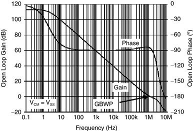
Figure 18.8 These typical performance curves show many of the parameters in the specification table of the data sheet of an amplifier. This graph illustrates the typical open-loop gain, phase vs. frequency response. The arrow in this figure points to the gain-bandwidth product for this unity-gain-stable amplifier.
The gain-bandwidth product (GBWP) will tell you the highest small-signal frequency (∼ ±100 mV) that you can send through your amplifier circuit without distortion. It also tells you the frequency where a pole is introduced to your closed-loop amplifier circuit. This is particularly critical to know when you design low-pass filters. In this type of circuit, you deliberately put poles in the transfer function by putting resistors and capacitors around the amplifier, as shown in Figure 18.2. If the amplifier adds a pole, your circuit could oscillate. Consequently, the closed-loop bandwidth of the amplifier must be at least 100 times higher than the cut-off frequency (fCUT-OFF) of the filter. Another way of stating this is that the gain-bandwidth product of your amplifier should be equal to or greater than 100 × fCUT-OFF (this assumes the filter has a gain of +1 V/V). If you don’t take these precautions, you might erroneously be inclined to investigate your filter equations only to find out that the amplifier is not well-suited for your design.
You might ask, “How important is this specification in other amplifier application circuits?” Generally, you will need an amplifier with good bandwidth performance for your signal, but probably won’t see instability because of your amplifier selection. Or in another application, you may be more concerned about the quiescent current of the amplifier or power supply capability instead of the bandwidth because you are designing a battery-powered circuit that operates at DC.
The second specification that I mentioned previously is slew rate. The slew rate of an amplifier is determined by putting a square wave signal at the input of the amplifier and looking to see how fast the signal changes on the output. The units of this specification are generally V/sec, V/msec, or V/μsec. You can find this specification in the table in the same way we found the gain-bandwidth product. There is also a characteristic curve in most amplifier data sheets that gives a good look at how a typical part will perform. You’ll find that the label of this graph is usually “Large signal, noninverting pulse response” (Figure 18.9).

Figure 18.9 This graph illustrates the typical time domain response of the output voltage vs. time of an amplifier.
With the filter circuit, this specification will tell you the maximum frequency of the large signals going through your circuit. If you don’t pay attention to this specification, you may find that the amplifier distorts your larger, higher frequency signals. A good rule of thumb for this design parameter is: slew rate ≥ (2πVOUT P-P × fCUT-OFF) where VOUT P-P is the expected peak-to-peak output voltage swing below fCUT-OFF of your filter.
18.2.3 Don’t Bother Me With the Small Stuff—Just Give Me the Data
One of the more common statements as said to me by the ambitious digital engineer is, “Just give me the data. I will fix it in my processor. I know we can design a digital filter with the classical FIR or IIR filters, or better yet implement an FFT response. I can also calibrate the signal if need be. I’m confident that I will be able to get rid of those undesirable, messy analog signals.”
This comment always brings a smile to my face. See the case in point with the circuit in Figure 18.10.
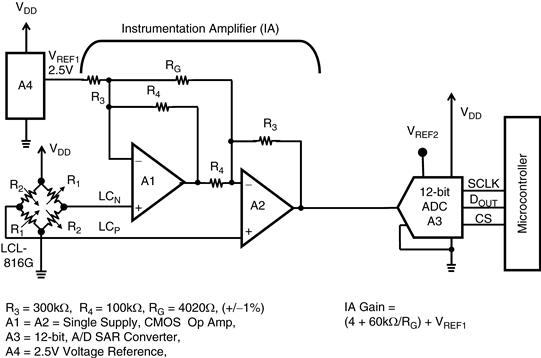
Figure 18.10 The circuit in this diagram uses a 12-bit A/D converter in combination with an instrumentation amplifier to convert the low-signal output of a Wheatstone bridge sensor to usable digital codes.
The analog portion of this circuit has a load cell, a dual-operational amplifier configured as an instrumentation amplifier, a SAR A/D converter, a microcontroller and voltage references for the IA and A/D converter. The sensor is a 1.2Ω, 2 mV/V load cell with a full-scale load range of ±32 ounces. In this 5V system, the electrical full-scale output range of the load cell is ±10 mV. The instrumentation amplifier, consisting of two operational amplifiers (A1 and A2) and five resistors, is configured with a gain of 153 V/V. This gain matches the full-scale output swing of the instrumentation amplifier block to the full-scale input range of the A/D converter. The SAR A/D converter has an internal input sampling mechanism. With this function, a single sample is taken for each conversion. The microcontroller acquires the data from the SAR A/D converter. The controller can also execute calibration and translate the data into a usable format for tasks such as displays or actuator feedback signals.
The transfer function, from sensor to the output of the A/D converter is:
![]()

where LCP and LCN are the positive and negative sensor outputs,
GAIN is the gain of the instrumentation amplifier circuit. The instrumentation amplifier is configured using A1 and A2. The gain is adjusted with RG,
VREF1 is a 2.5V reference which level shifts the instrumentation amplifier output;
VREF2 is a 4.096V reference, which determines the A/D converter input range and LSB size;
VDD is the power supply voltage and sensor excitation voltage;
DOUT is a decimal representation of the 12-bit digital output code of the A/D converter (rounded to the nearest integer).
If the design of this system is poorly implemented, it could be an excellent candidate for noise problems. The symptom of a poor implementation is an intolerable level of uncertainty with the digital output results from the A/D converter. It is easy to assume that this type of symptom indicates that the last device in the signal chain generates the noise problem. But, in fact, the root cause of poor conversion results could originate with other active devices or passive components in the signal chain, the PCB layout or even extraneous sources.
In this circuit, noise can be reduced within the analog channel hardware. But, with the first prototype of this circuit, these low noise precautions were not used. Therefore, the data output of the A/D converter illustrated in Figure 18.11 indicates that this was a noisy system. It is fine to design a proto with this level of noise. In addition, it is truly divine to understand the noise and remove it in hardware wherever possible.
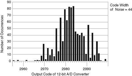
Figure 18.11 A poor implementation of the 12-bit data acquisition system shown in Figure 18.10 could easily have an output range of 44 different codes with a 2,048 sample size.
But, let’s assume that you take the digital route to perform the filtering. On a perfect day, you will need to collect at least 2,048 12-bit data points and calculate the average. I said on a perfect day because when I look at this data there seems to be more going on than just white noise. There are small occurrences in the lower 20 codes of the data, and the major portion of the data does not form a “normal distribution” type of curve. It seems to have troughs and there is nothing normal about this data at all.
A common, bad scenario is that the problem is never solved through the lifetime of your application circuit. These unknown noise problems are fixed with digital tricks. That overly confident statement ignores the trade-offs inherent in taking the all-digital route. One of the major consequences is time. A digital filter needs to collect several hundreds of samples in order to compete with the analog solution. On top of that, the already digitized signal has been contaminated by aliased high-frequency signals, and you will never be able to tell your original signal from the contaminants. These tricks may or may not work over time.
On the other hand, the analog solution is simple and final. The data loses its erratic behavior and you can get the same converted number every time! What do you do?
1. Put bypass capacitors across the power supply pin to ground with every active device.
2. Use a ground plane. This will usually require at least a two-layer board.
3. Reduce the resistor values in the instrumentation amplifier. When you reduce these resistors (without changing the throughput gain), the noise in the signal chain will also reduce.
5. Insert a low-pass filter before the A/D converter. This filter will remove higher frequency noise as well as eliminate aliasing problems.
6. Choke the power supply switching noise to the analog portion of the board with an inductor.
These are all simple solutions to a seemingly impossible, noisy circuit problem. Figure 18.12 shows the results of these actions.

Figure 18.12 When noise reduction techniques are used in the implementation of the circuit in Figure 18.10, it is possible to get a 12-bit system.
Calibration can be another sticky point when you go to the digital environment. Once you lose your dynamic range in the analog domain, it is impossible to recover it digitally. For instance, if you use amplifiers in this circuit that do not give you good rail-to-rail performance, the outer limits of the signal are lost forever. Another situation, not related to Figure 18.10, could occur if your signal is logarithmic instead of linear. If this is the case, digital manipulation will not take you very far. This type of data can only be fixed in the analog domain.
18.3 The Ultimate Key to Analog Success
News alert! The ultimate analog key does not exist. And I don’t mind turning this around to tell analog engineers that digital engineering is a little more than ones and zeros. The analog mountains that can be climbed are analogous to your digital challenges. Following are three examples.
For the first example, in the spirit of designing a robust design, the digital designer architects the software to identify unforeseen, catastrophic errors. The watchdog timer (WDT) can be used for this purpose. The function of a watchdog timer is easy enough. It counts down using the system clock from an initial value to zero. During implementation, if your firmware does not reset this timer soon enough, the watchdog timer resets or interrupts the system without human intervention when the counter reaches zero. Alternatively, the analog domain protection circuitry is used to minimize the effects of unforeseen errors or transients. In analog disciplines this can be implemented with over-range notifications or protection devices at sensitive nodes, such as zener diodes, metal oxide varistors (MOV), transzorbes, or Schottky diodes. With these types of additions to the hardware, “bad” signals are identified and eliminated before they become part of the signal path.
The second example would be to work on your digital design low-power strategies by effectively using clocking algorithms. Low power should be thought of as a “state of mind.” With a low-power mindset, you can throttle down your controller to near inactivity if you really want to save battery power. The hardware approach would be to reduce clock source rate or power supply voltage. An equally effective approach is to operate with a partial or complete controller/processor shutdown mode. Combining these techniques with execution time and a little intelligence, you can easily tackle your most challenging power conservation problems. In your analog design, you will choose the lower power devices and utilize device shutdown features. In this environment, the designer needs to research the market for the best solution, whether it is a similar lower power device, or an alternative silicon topology that runs more efficiently.
A third example would be where you savor and protect your programming tricks from your competition. You can do this by making the code unreadable in the finished product in the same way the analog engineer buries traces inside boards, blacks out device part numbers, or asks vendors to give him proprietary part numbers.
The list goes on. But the thing to remember and understand is that each of us, in our own disciplines, tries to take technology to its limit. So what do you do when your manager says in his one-sided conversational way, “You’re an engineer (aren’t you)? Good. Since we are understaffed, I need you to do the entire (hardware/software) design. What? You don’t know anything about analog. Hmmm, maybe I need to find someone else? I knew you would rise to the occasion. Have your development schedule on my desk by the end of the day so I can set up a deadline schedule.”
18.4 How Analog and Digital Design Differ
The basic difference between the analog mindset and digital mindset is embedded in the definitions of precision (calculated risk versus right every time), hardware versus software, and time (or the inverse of). The basic concepts behind analog and digital disciplines are easy to find. In terms of this chapter, I will describe analog design from a practical standpoint. You will find that the in-depth lists and details about product specifications will be a little thin, but there is a detailed discussion about key specifications as they relate to basic analog systems.
18.4.1 Precision
What is “precise enough” in an analog circuit? There are three ways to answer this question. A first aspect of accuracy is “as precise as it needs to be.” You will find that some of your circuits will only require accuracy to one or two millivolts. Others will require accuracy to the submicrovolts.
This difference in system requirements will encourage you to settle for “close enough” in some systems, and “What else can I squeeze out of this circuit?” in other systems.
A second aspect of accuracy involves really understanding the components and devices you are working with. In terms of the components, you should know that a 1 kΩ resistor or a 20 pF capacitor is not equal to those absolute values all the time. For instance, temperature can have a dramatic effect on these components. Also, there are variations from device-to-device out of your bin in the lab. The combination of these two major issues can change the performance of your circuit dramatically if you don’t take them into consideration.
In terms of devices, you will find product data sheets have maximum guaranteed values and typical values. The maximum guaranteed values are self-explanatory in that you should expect that your devices will not over-range the specifications as stated provided the devices are not overstressed with higher voltages or temperatures. The typical values are another manner. There are a variety of ways to determine what these typical values should be, and you will find that each manufacturer will have their own way to calculate these values along with their justification. Some manufacturers take the average of a large sample of devices prior to the initial product release. Other manufacturers define their typical values as being equal to one standard deviation plus the average. I have also heard of manufacturers using their Spice simulation as a guide for these numbers. Sometimes the Spice simulation is justified because it is impossible to test a particular specification.
The third aspect of accuracy is noise. When you take this issue into consideration, you need to have some understanding of statistical calculations with large samples.
18.4.2 Hardware versus Software
This discussion seems to simplify the problem a bit, but I have a solution for those embarking on the ownership of analog. Think of it in terms of learning the fundamentals about your components, knowing the general behavior of basic building-block devices, and running through a high-level evaluation of your circuits first.
For instance, the fundamentals at the very bottom of the barrel include resistors, capacitors and inductors. You were probably exposed to the devices early in your career, but what do you really need to know as an analog design engineer?
Resistors are simple devices. There are several perspectives that you have to consider when you use this type of component in your design. The first and easiest way of thinking about a resistor is that it influences voltage and current in your design. This is defined through the infamous Thévenin equation:
![]()
where V is voltage,
R is resistance in ohms,
I is current in amperes.
I always remember this formula from my elementary school geography lessons. Vermont is always over Rhode Island.
But this is only part of the resistor description in your circuit. For practical purposes, this is a DC equation, not AC. Moving past this formula, you need to be concerned about the parasitic characteristics. Namely, there is a parasitic capacitor in parallel with the resistive element and a parasitic inductor in series. These components are artifacts of the physical device. There is a diagram of the resistor with these parasitics in Figure 18.13.

Figure 18.13 This illustrates a typical resistor model. The parasitic elements of a standard resistor are parallel capacitance (CP) and series inductance (LS)
The fact is, I never worried about the parasitic capacitance until I started designing transimpedance, optical, photodiode-sensing circuits. An example of this type of circuit is shown in Figure 18.14. If blindly built (without concern for the parasitic capacitance), this photosensing circuit can mysteriously sing like a bird (oscillate) without too much effort. This oscillation is usually caused by an inappropriate choice of CF, but it can also be caused by that phantom capacitor, CP. These capacitors, in combination with the photodiode parasitic capacitance and the amplifier’s input capacitance interact to establish stability, or not. This is one example, but you can extrapolate this to other circuits if you are using small value discrete capacitors in parallel or series with discrete resistors.

Figure 18.14 If you don’t consider the parasitic capacitance of the feedback resistor, a transimpedance photosensing circuit can be unstable.
The parasitic inductance of the resistor (also see Figure 18.15) can affect higher speed systems where lower value resistors are the norm. This inductance can affect the behavior of the current sensing resistor used in switched-mode power supplies.

Figure 18.15 The impedance of a resistor changes from the defined DC resistance value to other values over frequency. The parasitic capacitance and impedance influence these changes.
Generally speaking, the impedance of higher value resistors is more affected by the parasitic capacitance, and that of low value resistors is affected by the parasitic inductance. Figure 18.15 illustrates this point.
Capacitors, on the other hand, should be considered in the frequency domain when you are designing. There is one formula for the capacitor that I used frequently in my design. This formula is:
![]()
where C is capacitance in farads,
δV is change in voltage in volts,
δt is change in time in seconds.
Capacitors are very useful for power supplies, stability, loading low dropout regulators and loading voltage references. But, in all cases, you use capacitors to modify frequencies, not DC signals.
2. Know the general behavior of basic building blocks. Consider these basic circuit cells as instruction codes. Start by using them in their most common circuit configurations or the classical approach. In analog, your basic building blocks are:

Figure 18.16 This illustrates a typical ceramic capacitor model. The parasitic elements of a standard capacitor are series resistance (Rs), also known as effective series resistance (ESR), and series inductance (Ls), also known as effective series impedance (ESL).

Figure 18.17 The frequency response of a capacitor varies at lower frequencies due to the series resistance and higher frequencies due to the series inductor.
– Analog-to-digital converters
3. Higher level thinking. Are you afraid of math? Don’t dwell on it at first. Concentrate on the practical side of analog applications. Learn the rules of thumb for analog. For instance, many of us, being indoctrinated in the school system background, sharpen our pencils, pull out the old calculator and grind through the trees before we have a thought about what the forest looks like. Once you step back and think about it, you will find that your detailed analysis can be way off. If your analysis is correct, it probably is only part of the picture. Here is a perfect example of what I mean.
Problem:
What is the corner frequency of the single-pole, low-pass RC filter shown in Figure 18.18?
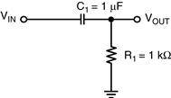
Figure 18.18 Circuit example
Answer
“Hand wave” solution: Wait a minute. This isn’t a low-pass filter. This is a high-pass filter. (You probably knew this right away, but you would be amazed at how many would overlook this simple conclusion!) But if I assumed that the author made a mistake and reversed the placement of the resistor and capacitor, the corner frequency would be about 1/(2 πR × C) or 160 Hz. How did I get there? Isn’t 1/2 π equal to about 0.16? As a first pass, I think I can accept that error because the capacitor device-to-device error is probably ±10 or 20% accurate.
Calculated solution (with blinders on):

From this calculation, there is a pole at DC and a zero at 159.1549 Hz.
These two solutions don’t agree! And I bet a SPICE simulation would match your calculated solution. The moral to this story is “hand wave,” or think yourself through the problem first. SPICE does not mean “don’t think,” it means “verification of your analysis.” With this type of analysis, you should keep in mind the accuracy (or lack thereof) of the various components and devices in your system. After, and only after, you know generally how the circuit works and how the system responds, give your mathematical and SPICE skills a try.
18.5 Time and its Inversion
In the digital domain, particularly with real-time operating systems (RTOS), you will find that you are counting minutes, seconds, milliseconds, and nanoseconds. This is also done with analog circuits, but more importantly, the inverse of seconds is counted. Taking the inverse of seconds helps you think in terms of frequency instead of time. Frequency information is much more critical here.
18.6 Organizing Your Toolbox
You need to decide what is important and what is not for your future analog design work. An effective way to do this is to arm yourself with basic, key tools of the trade. You should concentrate as you collect your ammunition on six topics.
First, know how to get data in and out of the digital domain. When this is mastered you will know the different topologies, important specifications, and the art of matching the converter to the application.
Then, sit back and ask yourself, “Where does my data in the controller really come from?” You will usually find some sort of sensor at the origin of the signal path. Further back from the A/D converter is the amplification system. In this system, the signal can either be enhanced through amplification or corrupted because of noise or linearity errors. The key player in the amplification system is the operational amplifier. Volumes of books have been written on this seemingly simple part, but not enough written about the single-supply operational amplifier applied in a simple manner.
Now go back to your strength. Revisit the digital with analog in mind. Can you exploit your digital engine easily with a few analog tricks?

Figure 18.19 This signal chain is somewhat universal in that it deals with the analog signal coming in, conditions it through the amplification system and digitizes it in preparation for the microcontroller or processor.
Go out on a limb. Bring the “art” of some of the essential analog disciplines into your toolbox. In particular, learn about noise sources and noise filters. Think about your layout and how it affects your circuit solution. Then go to the lab with confidence.
18.7 Set Your Foundation and Move On, Out of The Box
Drop your inhibition. Have fun. Work outside your box. Learning a new craft takes persistence, time and a learning attitude. Analog design is a matter of sitting down and doing it, whether it is right or wrong. Then on the next day tweak it, and the next day, and the next day, until the circuit is finally refined. No magic formulas here, just some common sense, and problem solving techniques. First, define the problem. Second identify tools and strategies that can be used to work the problem. Third, work the problem to a solution. Finally, reread your definition of the problem and determine if your solution seems reasonable. Analog only demands good, honest, consistent and persistent work. Sound familiar?
References
1. “FilterPro™.MFB and Sallen-Key Low-Pass Filter Design Program,” Bishop, Trump, Stitt, SBFA001A, Texas Instruments.
2. FilterLab®2.0 User’s Guide, DS51419A, Microchip Technology.
3. Marsh David. CANbus Networks Break Into Mainstream Use. EDN 2002.
4. Warner Will. Making the CANbus a “can-do” Bus. EDN 2003.
5. “Implementing Ohmmeter/Temperature Sensor,” Cox, Doug, AN512, Microchip Technology.
6. “Resistance and Capacitance Meter Using a PIC16C622,” Richey, Rodger, AN611, Microchip Technology.