
Chapter 17
Dealing with High-Speed Logic
Much has been written about terminating printed circuit board traces in their characteristic impedance to avoid reflections. A good rule of thumb to determine when this is necessary is: Terminate the line in its characteristic impedance when the one-way propagation delay of the PCB track is equal to or greater than one-half the applied signal rise/fall time (whichever edge is faster). A conservative approach is to use a 2-inch (PCB track length)/nanosecond (rise/fall time) criterion. For example, PCB tracks for high speed logic with rise/fall time of 1 ns should be terminated in their characteristic impedance if the track length is equal to or greater than 2 inches (including any meanders). Figure 17.1 shows the typical rise/fall times of several logic families including the SHARC DSPs operating on 3.3V supplies. As would be expected, the rise/fall times are a function of load capacitance.

Figure 17.1 Typical DSP output rise times and fall times
This same 2-inch/nanosecond rule of thumb should be used with analog circuits in determining the need for transmission line techniques. For instance, if an amplifier must output a maximum frequency of fmax, then the equivalent rise time, tr, can be calculated using the equation tr = 0.35/fmax. The maximum PCB track length is then calculated by multiplying the rise time by 2 inch/nanosecond. For example, a maximum output frequency of 100 MHz corresponds to a rise time of 3.5 ns, and a track carrying this signal greater than 7 inches should be treated as a transmission line.
Equation 17.1 can be used to determine the characteristic impedance of a PCB track separated from a power/ground plane by the board’s dielectric (microstrip transmission line):
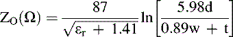 (17.1)
where εr = dielectric constant of printed circuit board material:
The one-way transit time for a single metal trace over a power/ground plane can be determined from Equation 17.2:
![]() (17.2)
(17.2)
For example, a standard four-layer PCB board might use 8-mil-wide, 1 oz. (1.4 mils) copper traces separated by 0.021″ FR-4 (εr = 4.7) dielectric material. The characteristic impedance and one-way transit time of such a signal trace would be 88W and 1.7 ns/ft (7″/ ns), respectively.
The best ways to keep sensitive analog circuits from being affected by fast logic are to physically separate the two and use no faster logic family than dictated by system requirements. In some cases, this may require the use of several logic families in a system. An alternative is to use series resistance or ferrite beads to slow down the logic transitions where the speed is not required. Figure 17.2 shows two methods. In the first, the series resistance and the input capacitance of the gate form a low-pass filter. Typical CMOS input capacitance is 5 pF to 10 pF. Locate the series resistor close to the driving gate. The resistor minimizes transient currents and may eliminate the necessity of using transmission line techniques. The value of the resistor should be chosen such that the rise and fall times at the receiving gate are fast enough to meet system requirement, but no faster. Also, make sure that the resistor is not so large that the logic levels at the receiver are out of specification because of the voltage drop caused by the source and sink current that flow through the resistor. The second method is suitable for longer distances (>2 inches), where additional capacitance is added to slow down the edge speed. Notice that either one of these techniques increases delay and increases the rise/fall time of the original signal. This must be considered with respect to the overall timing budget, and the additional delay may not be acceptable.

Figure 17.2 Damping resistors slow down fast logic edges to minimize EMI/RFI problems
Figure 17.3 shows a situation where several DSPs must connect to a single point, as would be the case when using read or write strobes bidirectionally connected from several DSPs. Small damping resistors shown in Figure 17.3(A) can minimize ringing provided the length of separation is less than about 2 inches. This method will also increase rise/fall times and propagation delay. If two groups of processors must be connected, a single resistor between the pairs of processors as shown in Figure 17.3(B) can serve to damp out ringing.
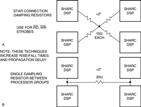
Figure 17.3 Series damping resistors for SHARC DSP interconnections
The only way to preserve 1 ns or less rise/fall times over distances greater than about 2 inches without ringing is to use transmission line techniques. Figure 17.4 shows two popular methods of termination: end termination, and source termination. The end termination method (Figure 17.4(A)) terminates the cable at its terminating point in the characteristic impedance of the microstrip transmission line. Although higher impedances can be used, 50Ω is popular because it minimizes the effects of the termination impedance mismatch due to the input capacitance of the terminating gate (usually 5 pF to 10 pF). In Figure 17.4(A), the cable is terminated in a Thévenin impedance of 50Ω terminated to 1.4V (the midpoint of the input logic threshold of 0.8V and 2.0V). This requires two resistors (90Ω and 120Ω), which adds about 50 mW to the total quiescent power dissipation to the circuit. Figure 17.4(A) also shows the resistor values for terminating with a 5V supply (68Ω and 180Ω). Note that 3.3V logic is much more desirable in line driver applications because of its symmetrical voltage swing, faster speed, and lower power. Drivers are available with less than 0.5 ns time skew, source and sink current capability greater than 25 mA, and rise/fall times of about 1 ns. Switching noise generated by 3.3V logic is generally less than 5V logic because of the reduced signal swings and lower transient currents.
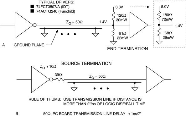
Figure 17.4 Termination techniques for controlled impedance microstrip transmission lines
The source termination method, shown in Figure 17.4(B) absorbs the reflected waveform with an impedance equal to that of the transmission line. This requires about 39Ω in series with the internal output impedance of the driver, which is generally about 10Ω. This technique requires that the end of the transmission line be terminated in an open circuit; therefore no additional fanout is allowed.
The source termination method adds no additional quiescent power dissipation to the circuit.
Figure 17.5 shows a method for distributing a high speed clock to several devices. The problem with this approach is that there is a small amount of time skew between the clocks because of the propagation delay of the microstrip line (approximately 1 ns/7″). This time skew may be critical in some applications. It is important to keep the stub length to each device less than 0.5″ in order to prevent mismatches along the transmission line.
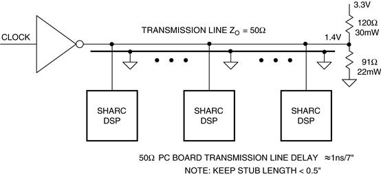
Figure 17.5 Clock distribution using end-of-line termination
The clock distribution method shown in Figure 17.6 minimizes the clock skew to the receiving devices by using source terminations and making certain the length of each microstrip line is equal. There is no extra quiescent power dissipation, as would be the case using end termination resistors.
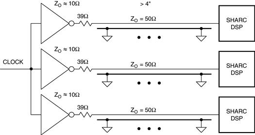
Figure 17.6 Preferred method of clock distribution using source terminated transmission lines
Figure 17.7 shows how source terminations can be used in bidirectional link port transmissions between SHARC DSPs. The output impedance of the SHARC driver is approximately 17Ω, and therefore a 33Ω series is required on each end of the transmission line for proper source termination.
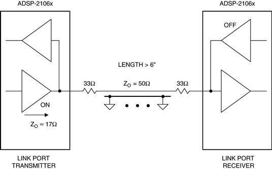
Figure 17.7 Source termination for bidirectional transmission between SHARC DSPs
The method shown in Figure 17.8 can be used for bidirectional transmission of signals from several sources over a relatively long transmission line. In this case, the line is terminated at both ends, resulting in a DC load impedance of 25Ω. SHARC drivers are capable of driving this load to valid logic levels.

Figure 17.8 Single transmission line terminated at both ends
References on Dealing with High Speed Logic
1. Johnson Howard W, Graham Martin. High-Speed Digital Design PTR Prentice Hall 1993.
2. EDN . EDN’s Designer’s Guide to Electromagnetic Compatibility. January, 20, 1994.
3. Designing for EMC (Workshop Notes). Kimmel Gerke Associates, Ltd. 1994.
4. Montrose Mark. EMC and the Printed Circuit Board IEEE Press 1999; (IEEE Order Number PC5756).