
Chapter 13
Selecting a Design Route
13.1 Introduction
This chapter describes the various design routes that can be used to implement a circuit design. The decision regarding which of these design routes to use depends upon the following issues:
• When should the first prototype be ready?
• What are the power requirements?
• What is the budget for the product?
• What are the physical size limitations?
• How complex is the design (gate count, if known)?
• What is the maximum frequency for the design?
• What loads will the system be driving?
• What other components are needed to complete your design?
• What experience have you or your group had to date in the design of digital systems?
These are the questions that must be asked before starting any design. The aim of this chapter is to provide background to the various design routes that are available. Armed with this knowledge, the answers (where possible) to the above questions should allow the reader to decide which route to select or recommend.
13.1.1 Brief Overview of Design Routes
The various design options are illustrated in Figure 13.1. As can be seen, the choice is either to use standard products or to enter the world of application-specific integrated circuits (ASICs). The “standard product” route is to choose one, or a mixture, of the logic families such as 74HCT, 74LS, 4000 series, etc. On the other hand, an ASIC is simply an IC customized by the designer for a specific application. Various ASIC options exist that can be subdivided into either field-programmable or mask programmable devices. Field-programmable devices (i.e., ROM, PAL, PLA, GAL, EPLD, and FPGA) are all programmed in the laboratory. However, mask programmable devices must be sent to a manufacturer for at least one mask layer to be implemented. These mask programmable devices may be exclusively digital or analog, or alternatively what is known as a mixed ASIC, which will contain both.

Figure 13.1 Design options
The mask programmable devices can be further subdivided into full custom, standard cell and gate array. With full custom design, the designer has the option of designing the whole chip, down to the transistor level, exactly as required. Standard cell design again presents the designer with a clean slice of silicon but provides standard cells (e.g., gates, flip-flops, counters, op-amps, etc.) in a software library. These can be automatically positioned and connected on the chip as required (known as place and route). Both of these levels of design complexity are used for digital and analog design, and are characterized by long development times and high prototyping costs. The third and lowest level in terms of complexity is the gate array. With the gate array, the designer is presented with a “sea” of universal logic gates and is required only to indicate how these gates are to be connected, which then defines the circuit function. This approach offers a less complex, and hence cheaper, design route than standard cell and full custom.
Until the late 1980s, the cheapest route to a digital ASIC was via the use of a mask programmable gate array. These devices are still widely used, but since the late 1980s, have had to face strong competition from field-programmable gate arrays (FPGAs) where the interconnection and functionality are dictated by electrically programmable links, and hence appear in the field-programmable devices section.
With regard to the previous ten questions, the overriding issue is usually when the first prototype should be ready. ASICs require computer-aided design (CAD) tools of differing complexities. Designs that use such tools provide elegant solutions, but can be very time consuming especially if your team has no experience in this field. However, designs that use “standard products” are quick to realize but can be bulky and expensive when high volumes are required.
With the exception of microcontrollers/processors and DSPs, this chapter will describe the design options in Figure 13.1 in more detail. However, it should be noted that as… you move from left to right across this diagram, each option becomes more complex to implement resulting in a longer design time and greater expenditure.
13.2 Discrete Implementation
The 74 series offers a whole range of devices at various levels of integration. These levels of integration are defined as:
• SSI – Small-scale integration (less than 100 transistors per chip);
• MSI – Medium-scale integration (100–1,000 transistors per chip);
• LSI – Large-scale integration (1,000–10,000 transistors per chip);
• VLSI – Very large-scale integration (greater than 10,000 transistors per chip).
The VLSI devices are mainly microcontrollers and microprocessors which are outside the scope of this book.
Designs using these standard parts are quick to realize and relatively easy to debug. However, they are bulky and expensive when high volumes are required. The various functions available allow all sorts of digital systems to be implemented with minimal overheads and tooling. For expediency these designs can be ad hoc and incorporate poor digital design techniques. We shall look at some of these pitfalls and suggest alternative safe design practices.
One such standard product is the 74HCT139 which consists of two 2-to-4 decoders in a single IC package. A logic diagram for this IC is shown in Figure 13.2. A decoder can be used in memories for addressing purposes where only one output goes high for each address applied. Such a device has many other uses. However, one must be careful with this type of circuit since any of the decoder outputs can produce spurious signals called static hazards. These static hazards are called spikes and glitches.

Figure 13.2 74HCT139: two-to-four decoder
13.2.1 Spikes and Glitches
Consider the case of output Y3 in Figure 13.2. A timing diagram is shown in Figure 13.3 for this output for various combinations of A and B. At first AB = 00 and so Y3 = 0. Next, AB = 10 and Y3 goes high. With AB returning to 00 the output goes low again. All seems satisfactory so far but if AB = 11, then due to the propagation delay of the inverter the output will go high for a short time equal to the inverter propagation delay. As we shall see, although this spike is only a few nanoseconds in duration, it is sufficiently long enough to create havoc when driving clock lines and may inadvertently clock a flip-flop. This phenomenon is not limited to decoders. All combinational circuits will produce these spikes or glitches.

Figure 13.3 Spike generation on output Y3 of the 2-to-4 decoder
To appreciate the problem when driving clock lines, consider a circuit counting the number of times a four-bit counter produces the state 1001. A possible design using 74 series logic is shown in Figure 13.4(A). This consists of a 4-to-16 decoder (74HC154)1 being used to detect the state 1001 from a four-bit counter (74HC161). (For clarity the four-bit counter output connected to the four inputs of the decoder is represented as a data bus having more than one line. The number of signals in the line is indicated alongside the bus.) The 10th output line of the decoder is used to clock a 12-bit counter (74HC4040). However, although this will detect the state 1001 at the required time, it will also detect it at other times due to the differing propagation delays in the 4-to-16 decoder. These spikes and glitches will trigger the larger counter and result in a false count. There are two solutions to this: an elegant one and one that some undergraduates fall mercy to! The latter method, illustrated in Figure 13.4(B), is to use an RC network (connected as an integrator or a low-pass filter) and a Schmitt trigger which together remove the spike or glitch. The values of R and C are chosen so as to filter out this fast transient—usually RC is set to be 10 times the glitch or spike pulse width. Due to this long time constant, the signal presented at the input to the Schmitt is now only a fraction of the magnitude of the original spike. To remove this signal completely it is passed through a Schmitt. This device has a voltage transfer characteristic which has two switching points. When the input is rising (from 0V) the Schmitt switches at typically 0.66 Vdd. However, when the input is falling (from Vdd) the Schmitt now switches at 0.33 Vdd. Hence any signal that does not deviate by more than two-thirds of the supply will be removed. This circuit, although successful, cannot be used in any of the other design options in this chapter since large values of R and C are not provided on chip. In addition, the provision of extra inputs and outputs for these passive components will produce an unnecessarily large chip. The elegant solution, shown in Figure 13.4(C), is to detect the previous state with the decoder and present this to the D input of a D-type. The clean output of the flip-flop is then used to drive the 12-bit counter.

Figure 13.4 Using a decoder as a state detector. (A) Unsafe clocking of 12-bit counter; (B) Poor technique for correcting (A) – [RC>>spike/glitch width]; (C) Safe clocking technique
To summarize, an important rule for all digital designers is that clock inputs must not be driven from any combinational circuit, even a single two-input logic gate. This can be stated quite succinctly as no gated clocks. In fact the same is true for reset and set lines since these will also respond to spikes and glitches, thus causing spurious resetting of the circuit.
13.2.2 Monostables
Another tempting circuit much frowned upon by the purist is the monostable. The monostable or “one shot” produces a pulse of variable width in response to either a high-to-low or a low-to-high transition at the input. The output pulse width is set via an external resistor and capacitor.
One application of the use of a monostable is shown in Figure 13.5(A). Suppose that we require an eight-bit parallel-in, serial-out (PISO) shift register to be loaded with an eight-bit data word when a line called interrupt goes high. An active high load signal must be produced that will load the eight-bit data. This load signal must be returned low before the next rising clock edge so that serial data can continue to be clocked out. It should be noted that in this case the interrupt line is assumed to be synchronized with the clock. By adjusting the value of R and C the required parallel load pulse width (kRC, where k is a constant) is set to be no longer than the clock pulse width less the load to clock set-up time. The corresponding timing diagram is shown in Figure 13.5(B).
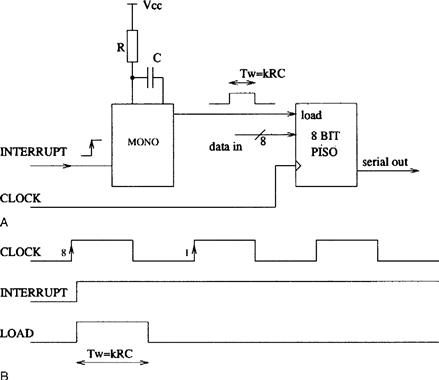
Figure 13.5 Use of a monostable to produce a short pulse
However, circuits that use monostables exhibit several limitations. The first is that it is necessary to use an external R and C, which will require a redesign when migrating to an ASIC. Other problems related to the analog nature of the device are: the pulse width varies with temperature, Vcc and from device to device; poor noise margin thus generating spurious pulses; oscillatory signal edges are generated for narrow pulse widths (less than approximately 30 ns); and long pulses require large capacitors, which are bulky.
An alternative to the circuit in Figure 13.5(A) is to use the circuit in Figure 13.6(A), which uses the reset technique with a purely digital synchronous approach. The resulting timing diagram for this circuit is shown in Figure 13.6(B). The circuit operates by using a clock frequency of twice the PISO register clock (2-clock). When interrupt goes from low to high, Q 1 (i.e., load) will go high. This will load in the parallel data. At the next rising 2-clock edge Q2 goes high (as its input, Q1, is now high) and clears or resets the load line. Because of the higher clock frequency used, this all occurs within half a clock cycle. A divide-by-two counter is used to divide 2-clock down to clock so that the new data loaded into the PISO can be serially shifted out on the immediately following rising edge of clock. Load will not go high again until another low to high transition on interrupt occurs.

Figure 13.6 Alternative circuit to the monostable circuit in Figure 13.5
The following example shows how pulses of a longer time duration can be produced.
Example 13.1
Consider the circuit in Figure 13.7. What pulse width is produced at the Q output of the D-type (74HC74) device? Assume that both “CLR” and “RESET” are active high.

Figure 13.7 Circuit to produce a controlled long pulse width
Solution
When a BEGIN low-to-high transition occurs, the Q output goes high, which releases the counter from its reset position. The counter proceeds to count until the Q11 output goes high, at which point the D-type flip-flop is cleared and the Q output goes low again awaiting the arrival of the next BEGIN rising edge. The Q output is thus high for 210 clock pulses.
Taking the clear input from any of the other outputs of the counter will produce pulses of varying width. The higher the input clock frequency, the better the resolution of the pulse width.
It should be noted that if BEGIN is synchronized with the clock then the rising edge of the output pulse will also be synchronized (albeit delayed by one D-type flip-flop delay). However, the falling edge of the Q output pulse is delayed with respect to the clock. This is because the counter used is an asynchronous or ripple counter. The Q11 output will only go high after the clock signal has passed through 11 flip-flop delays—this could be typically 100–400 ns. This may not cause a problem but is something to be aware of. The solution is to use either a synchronous counter or detect the state before with a 10-input decoder and a D-type as described earlier.
Example 13.2
The circuit of Figure 13.6(A) was designed in an ad hoc manner with the reset technique. Using state diagram techniques as discussed earlier produces a circuit that will implement the same timing diagram of Figure 13.6(B).
Solution
The first task is to use the timing diagram of Figure 13.6(B) to produce a state diagram. At the bottom of Figure 13.6(B) are the states A and B at each rising 2-clock edge. Remember, that the interrupt (I) line is generated by 2-clock (i.e., synchronized) and thus changes after the 2-clock rising edge. Hence the state diagram, shown in Figure 13.8(A), can be drawn. The corresponding state transition table is shown in Figure 13.8(B) and, since there are only two states, then only one flip-flop is needed. Assigning A = 0 and B = 1 results in Figure 13.8(C). From this we produce the K-maps for the next state Q+ and present output LOAD(L). These produce the functions Q+ = I and L = Q¯. The resulting circuit diagram is shown in Figure 13.8(E). It should be remembered that the clock input is the higher frequency 2-clock.

Figure 13.8 Using a state diagram to implement the timing diagram of Figure 13.6(B); (A) State diagram; (B) State transition table; (C) State assignment; (D) Mapping; (E) Circuit realization
13.2.3 CR Pulse Generator
The practice of using monostables has already been frowned upon and safe alternative circuit techniques have been suggested. However, monostables are tempting, quick to use and can still be found in many designs. Another design technique that is also simple and tempting to use but should be avoided is the CR pulse generator or differentiator circuit shown in Figure 13.9(A). The circuit is the opposite of the integrator shown in Figure 13.4. This circuit is used to “massage” a long pulse into a shorter one and so gives the appearance of a one-shot reacting at either rising or falling edges. If a 5V pulse is applied to the circuit in Figure 13.9(A) two short pulses are produced, one at the rising edge and one at the falling edge. At the rising edge when the input goes instantaneously from 0V to 5V the output momentarily produces 5V. As the capacitor charges the voltage across the resistor starts to fall as the charging current falls, hence the corresponding rising edge waveform. When the input changes from 5V to 0V the capacitor cannot change its state instantly and so both plates of the capacitor drop by 5V. Hence, the output momentarily produces −5V. The capacitor then discharges, resulting in the falling edge waveform.

Figure 13.9 Using a CR network to produce a narrow pulse
To convert this signal into a digital form the output is fed into a Schmitt trigger and thus produces a short pulse from 5V to 0V whose duration is determined by the value of R and C and the Schmitt switching point. This pulse is only present on the rising edge of the input since the falling edge produces a negative voltage, which the Schmitt does not respond to. However, this circuit should again be avoided as the migration to an ASIC would require a redesign while in addition the negative voltage may in time damage the Schmitt component. Consequently, it is therefore recommended that the pulse shortening techniques described earlier, which use a higher clock frequency, be employed.
13.3 Mask Programmable ASICs
The use of standard products (74 series, etc.) to implement a design becomes inefficient when large volumes are required. Hence, the facility for the independent customer to design their own integrated circuits was provided by IC manufacturers. This required the designer to use either a gate array, standard cell or full custom approach. In each case the manufacturer uses photomasks (or electron-beam lithography) to fabricate the devices according to the customer’s requirements. Therefore, these devices are… collectively named mask programmable ASICs.
13.3.1 Safe Design for Mask Programmable ASICs
A limitation of mask programmable ASICs is that, since the layers are etched using these masks, any design errors require a completely new set of masks. This is very expensive and time consuming and hence safe design techniques which work first time must be employed. A designer must avoid monostables and CR/RC type circuits and be aware that a manufacturing process can vary from run to run and sometimes across a wafer. Consequently, propagation delays vary quite considerably from chip to chip or even across a chip. Hence, the use of gates to provide a delay (see Figure 13.10(A)) is a poor design technique since the value of this delay cannot be guaranteed. Three poor ASIC circuit techniques where these delay chains are used are shown in Figs. 13.10(B)–(D). Essentially the designer must use synchronized signals and a higher clock frequency to generate short predictable pulses.
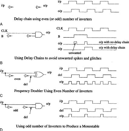
Figure 13.10 Examples of poor ASIC circuit techniques
The use of synchronous techniques is not a panacea for all timing problems. Take for example the master clock in a synchronous system driving several different circuits. The total capacitance being driven by the master clock can be extremely large, thus delaying the clock quite considerably. In order to isolate this large capacitance from the master clock, buffers are used leading to each circuit. These are quite simply two CMOS inverters in series. This reduces the capacitance seen directly by the master clock circuit and hence reduces the clock delay to each circuit. However, the input capacitance between the smallest and largest of these circuits may differ by an order of magnitude. Hence, the clock will arrive at different times to each of these circuits and the whole system will appear asynchronous in nature, A better buffering technique is therefore required. Two improved buffering techniques are shown in Figs 13.11(A) and (B). The first is to use an even number of inverters driving the large load. At first it just looks like our poor delay line shown in Figure 13.10(A). However, each inverter is larger than the previous one by a factor f (i.e., the W/L ratios of the MOS transistors are increased by f at each stage). The load capacitance gradually increases at each stage but the drive strength also increases. The optimum value of f is in fact e or 2.718, but the number of stages required for this case would be quite large. A compromise is to use an increased value of f and a reduced number of stages. Another technique is to use tree buffering which consists of several small inverters arranged in a tree structure. This is illustrated in Figure 13.11(B). In this case each inverting buffer is arranged such that it drives the same load. Hence, the relative clock signal delay will be kept to a minimum.

Figure 13.11 Two techniques for buffering the ASIC clock driver from a large capacitance
Example 13.3
One of the small inverters in Figure 13.11(B) is used to drive 64 loads each of 1 pF. Determine the delay of this inverter when driving this load directly and what the delay would be if the tree buffering of Figure 13.11(B) is used. Assume that the inherent delay of a single inverter is 1 ns, its output drive capability is 20 ns/pF and it has an input capacitance of 0.01 pF.
Solution
Unbuffered
![]()
Buffered

A great saving in delay is achieved at the expense of more gates.
Therefore, these safe mask programmable ASIC design techniques can be summarized as follows:
4. use synchronous techniques wherever possible;
In the early days, ASIC designs were breadboarded (i.e., a hardware prototype was produced) using 74 series devices in order to confirm that the design functioned correctly. However, nowadays the designer has available very accurate computer simulators that can be run in conjunction with drawing packages and chip layout. Together these computer programs are called computer-aided design (CAD) tools. Since a mask programmable ASIC cannot be modified once fabricated without incurring additional charges, the design cycle relies very heavily upon these CAD tools. The process of fabricating a chip and then finding a design fault is an unforgivable and costly error. We shall look at the various CAD tools employed to guarantee a “right first time” design.
13.3.2 Mask Programmable Gate Arrays
The first mask programmable ASIC that we shall look at is the mask programmable gate array. This device consists of a large array of unconnected blocks of transistors called gates. All the layers required to form these gates are prefabricated except for the metal interconnect. The IC manufacturer therefore has a “stock-pile” of uncommitted wafers awaiting a metal mask. The user or designer only needs to specify to the manufacturer how these gates are to be connected with the metal layer (i.e., customized).
The basic building block or gate in a CMOS gate array is a versatile cell consisting of four transistors. These blocks of four transistors are repeated many times across the array. Mask programmable gate arrays are characterized in terms of the number of four transistor blocks or gates in the array. The gate is called a versatile cell since it contains two NMOS and two PMOS transistors which can form simple logic gates such as NOR and NAND.
Two types of arrays exist—channelled and sea of gates. These are illustrated in Figures 13.12(A) and (B). The channelled array has a routing channel between each row of gates. These routing channels allow metal tracks on a fixed pitch to be used for interconnection across the array. Each channel can contain typically 20 wiring routes. The sea of gates on the other hand does not contain any dedicated routing channels and as a result contains more gates. The routing is implemented across each gate at points where no other metal exists. However, with the sea of gates the routing over long distances is more difficult and hence places a limit on the number of gates that can be accessed. This raises the important issue of utilization. This is the percentage of gates which the designer can access. As more gates on the array are utilized the routing ability for both array types is reduced. There comes a point where there are not enough routes available to complete the design and because of this manufacturers quote a utilization figure. As you can imagine, the channelled array has a better utilization than the sea of gates. A simple single layer metal channelled array has a utilization of 80% while a double layer metal has a utilization of 95%. Many mask programmable gate array manufacturers use three and four layer metal processes in order to fully utilize the array.

Figure 13.12 Channelled and sea of gates mask programmable gate arrays; (A) Channelled array; (B) Sea of gates array
For any design it is the gate count that is the most important issue. It is therefore useful to know how many gates typical functions consume in CMOS technology. For example a two-input NOR or NAND uses one gate, while a D-type and a JK consume five and eight gates, respectively. Hence, if a design schematic exists, then a quick gate count is always useful to specify what gate array size to use. The selection of an optimum array size is crucial in gate array design since array sizes can vary from 1,000 to 500,000 gates!
The cost of a mask programmable gate array depends upon:
1. number of gates required (or the number of I/Os);
2. number of parts required per year;
All mask programmable gate array, manufacturers charge a tooling cost for production of the metal mask(s). This charge is called a nonrecurring expenditure or NRE. Quotes from three reputable ASIC suppliers for a 2000-gate design, commercialized by the authors, revealed the following prices on a small volume of 1000 parts per year:
• Firm X (2 micron) NRE of £10000 at £4.00 unit cost;
The numbers in brackets indicate the minimum feature size on the chip, which is inversely proportional to the maximum operating frequency. Although the products are not fully comparable, one can see that the costs of mask programmable gate arrays involves the user in large initial charges, hence the importance of accurate CAD simulator tools prior to mask manufacture.
Because the gate array wafers before metallization are customer independent, the costs up to this stage are divided among all customers. It is only the metallization masks that are customer dependent and so these costs make up the bulk of the NRE. These NRE charges can be greatly reduced by sharing the prototyping costs even further by using a technique called a multiproject wafer (MPW). This is a metal mask that contains many different customer designs. The NREs are thus reduced approximately by a factor of N where N is the number of designers sharing that mask. Hence, prototyping costs with mask programmable gate arrays are less of a financial risk when a manufacturer offers an MPW service. The typical prototyping costs for a 2000 gate design, with MPW, are now as low as £1000 for 10 devices.
Of all the mask programmable ASICs the gate array has the fastest fabrication route, since a reduced mask set is required depending upon the number of metal layers used for the interconnect. The typical time to manufacture such a device (referred as the turnaround time) is four weeks.
Example 13.4
How many masks are needed for a double layer metal, mask programmable gate array?
Solution
The answer is not two since it is necessary to insulate one metal layer from the next and provide vias (holes etched in the insulating layers deposited between the first and second layer metal) where connections are needed between layers. Hence, the number is three, i.e., two metal masks and one via mask.
Example 13.5
A schematic for a control circuit consists of four 16 bit D-type based synchronous counters, 20 two-input NAND gates and 24 two-input NOR gates. Estimate the total number of gates required for this design.
Solution
Gate count for each part:
A 16-bit synchronous counter contains 16 D-type bistables plus combinational logic to generate the next state. This logic is typically comparable to the total gate count of the bistable part of the counter. Hence, the total gate count for the counter will be approximately 160 gates (i.e., 16 × 5 × 2). A two-input NAND gate will require four transistors and hence one gate. Thus, 20 will consume 20 gates of the array. Finally a single two-input NOR gate can be made from four transistors. Hence 24 will consume 24 gates of the array.
The total gate count required for this control circuit is 160 + 20 + 24 = 204 gates.
13.3.2.1 CAD Tools for Mask Programmable Gate Arrays
A mask programmable gate array cannot be modified once it has been fabricated without incurring a second NRE. Consequently a large reliance is placed upon the CAD tools, in particular the simulator, before releasing a design for fabrication. The generic CAD stages involved in the design of both mask- and field-programmable ASICs are illustrated in Figure 13.13. For mask programmable gate arrays this design flow is discussed below:
1. System description. The most common way of entering the circuit description is via a drawing package, called schematic capture. The user has a library of components to call upon, varying in complexity from a two-input NAND gate through to counters/decoders, PISO/SIPOs and arithmetic logic units. At no stage does the designer see the individual transistors that make up the logic gates. For large circuits (greater than approximately 10,000 gates) the description of the circuit using schematic capture becomes rather tedious and error prone. Consequently high-level, textual, programming languages have been developed to describe the system in terms of its behavior. The one language adopted as a standard is that recommended by the USA Department of Defense called VHDL. A brief introduction to VHDL is presented later in this chapter.
If the system is described in schematic form it is then converted into a netlist. This is a textual description of how the circuit is interconnected and is needed for the simulator. If the system is described in VHDL form, then for the sake of brevity this can be considered as a netlist description already.
2. Prelayout simulation. Once the system has been described, the next stage is to simulate the system prior to layout. The components used in the schematic or VHDL are represented as digital (or behavioral) models. A digital simulator, called an event-driven simulator, is used to simulate the system by applying input vectors to the system, i.e., a stream of 1s and 0s. This simulator obtains its name since only the gates whose inputs are changing (i.e., an event is occurring) are updated. The outputs then drive other gates and hence a new event is scheduled some time later. In some cases, to simplify the simulation, all gates are assumed to have a 1-ns delay or a unit delay and wire delays are set at zero. This is because the chip has not been laid out and therefore no information is available yet about wire delays. This type of simulation is called in some CAD manuals functional simulation. It is, however, advisable to simulate with the gate propagation delays which include fan-out loading, thus allowing the simulator to perform more realistic flip-flop timing checks such as: set-up and hold times; minimum clock and reset pulse widths, etc. This will identify, early in the design cycle, poor design techniques such as asynchronous events which violate set-up and hold time, or gated clocks which are revealed as spikes and glitches on clock lines.
3. Layout. Next, the chip is laid out and this consists of a two-stage process of place and route. First the gates used to describe the system are placed on to the array and implemented using the versatile four-transistor cell. Optimum placement algorithms are run which aim to reduce the total wire length. The cells are then connected together by using the available routing channels. The I/O positions may be left to the software to decide on the best position so as to assist the place and routing software, or may be specified by the user at the placement stage.
4. Back annotation of routing delays. The metal used for the interconnect contains resistance and capacitance and will introduce delays. Hence, these delays need to be added to the original system description, i.e., the schematic or VHDL file. This step is called back annotation and these extra delays are referred to as wiring parasitics.
5. Postlayout simulation. The performance of the original prelayout system will now have changed, which in some cases may result in the delays increasing from 1 ns to 100 ns. The system therefore needs to be resimulated with the parasitic delays included. This final simulation is called postlayout simulation and includes the timing delays of both the wiring and logic gates. The simulation is now called a full timing simulation since the true delays of the chip are included.2 Any errors appearing in the simulation at this stage must be corrected by modifying the original schematic or VHDL file and rerunning the layout. This iterative process is characteristic of all ASIC CAD design tools.

Figure 13.13 Generic CAD stages involved in the design of ASICs
An example of a layout-induced timing error is demonstrated with a two-stage shift register in Figure 13.14. The delay element indicated by the dotted box represents additional wire delay on the clock line. If this delay is greater than the propagation delay of the flip-flop, then data is lost. This is because when a shift register shifts data it is assumed that all clocks arrive at the same time at each flip-flop. However, if a clock arrives at the first flip-flop before the second by at least one flip-flop delay, then the data at the input to the second flip-flop will change before the arrival of its clock pulse. This data has been overwritten and therefore lost. To avoid this problem occurring, the place and route software allows the designer to influence the layout in several ways. Firstly, the clock line can be given priority (called seeding) and it is routed first before all the other routes. It will therefore have the shortest and hence the fastest path. Another technique is to label groups such as shift registers so that they are not broken up during placement. All flip-flops are consequently placed close to each other and hence clock delays are reduced.
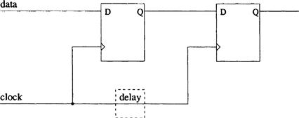
Figure 13.14 Layout delays on clock lines can cause a shift register to malfunction
When the postlayout simulation has been successfully completed, the designer has to pass an intensive sign-off procedure, which needs to be countersigned by the project manager and an engineer at the ASIC manufacturer. The final file that is passed to the manufacturer is in a syntax which is applicable for mask manufacturing machines and allows the metal interconnection layer(s) to be added to the base wafers in order to customize the array.
The CAD tools described here are either supplied by the IC manufacturer or by generic CAD software houses such as Mentor and Cadence. These tools take a design from schematic through to layout. Alternative tools, such as Viewlogic, are used for just the prelayout stage. These so-called front end tools are popular PC-based commodities and are used extensively in FPGA design.
13.3.3 Standard Cell
The advantages of fast turnaround time and relatively low cost offered by gate arrays are counterbalanced by several problems. The first is that silicon is wasted because a design does not use all the available gates on the array. Also, it is not known by the manufacturer which pad on the array is to be an input or an output and so silicon is further wasted by the inclusion of both input and output circuits at every pad. As the chip price is proportional to die size, then this can be uneconomical when large volumes are required. In addition, because all the transistors in a gate array are the same size, when transistors are placed in series long delays occur. This happens on the PMOS chain for NOR and the NMOS chain for NAND. Consequently the gates cannot be optimally designed and the delays τplh and τphl are asymmetrical. If the W/L’s of the transistors were individually adjusted for each gate type, the delays would be shorter.
The standard cell approach gets around these problems. Here, the designer again has available a library of logic gates but the design starts with a clean piece of silicon. Hence, only those gates selected for a design appear on the final chip and no silicon is wasted. It is also known which pads are to be input and output thus further saving silicon. The standard cell chip is therefore smaller than the gate array. This device is also faster partly because it is smaller and the routing is shorter (hence smaller wire delays) and partly because the library of logic gates is optimally designed by the manufacturer. This is achieved by adjusting the W/L’s of the transistors in each gate so as to achieve optimum delay.
Since the standard cell only uses those gates that are needed for a design, then each chip is of different size and is unique. Hence, all masks are required, which can be of the order of 8–16 masks where each mask costs £1000–£2000! The NRE costs are therefore considerably higher and the production times longer compared to a mask programmable gate array. This approach is therefore only economical when relatively large volumes are involved. However, reduced prototyping costs are again available by using multiproject wafers.
Libraries for standard cell (and gate arrays) have become quite sophisticated. Not only are the basic and complex gates provided but also counters and UARTs (serial interface) exist. Incredibly some manufacturers are even offering complete processor cores such as the Z180 by VLSI Technology, TMS320C50 by TI and the 80486 by SGS Thomson.
Example 13.6
Compare the transistor count of a complex combinational gate that is offered in the manufacturer’s library that produces the function ![]() implemented in a mask programmable gate array with a standard cell approach.
implemented in a mask programmable gate array with a standard cell approach.
Solution
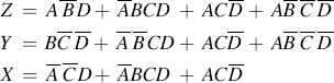
The gate array approach would require De Morgan’s theorem to implement this function using the blocks of four transistors (i.e., using either two-input NAND or two-input NOR gates). Choosing NAND gates results in:
![]()
The function using NAND gates is shown in Figure 13.15(A). Note that it is not possible to directly produce an AND gate with CMOS. This must be produced by using a NAND with an inverter. Thus the total number of gates required is 3.5 or 14 transistors.
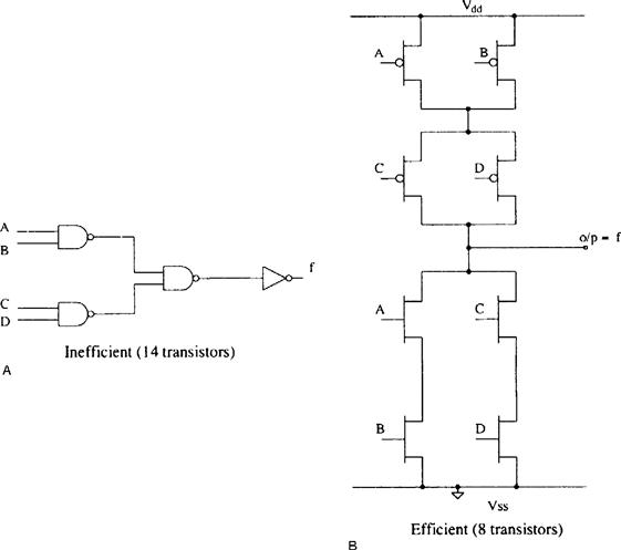
Figure 13.15 Inefficient and efficient implementation of the function ![]()
Consider now the standard cell. To implement the above function the library designer uses the following technique:
1. Concentrate on the NMOS network first: those terms that are AND’d are placed in series while those OR’d are placed in parallel.
The final circuit diagram is shown in Figure 13.15(B). Notice that the number of transistors used is now only eight, a great saving on silicon. In addition the gate array approach uses a three-level logic while the standard cell uses only a single level, giving the gate a much smaller propagation delay.
13.3.3.1 CAD Tools for Standard Cell
The CAD tools for a standard cell follow those for mask programmable gate arrays with a slight exception at the layout stage. Here the designer can interconnect each cell without the restriction of a fixed number of routing channels. This results in a chip that is much easier to route but may cause errors in the layout due to incorrect connectivity caused by designer intervention. To avoid this problem the designer has available layout verification tools which perform various checks on the layout. These are shown dotted in Fig 13.13 and consist of: design rule check (DRC), where the spacing of the metal interconnect is checked; electrical rule check (ERC), where the electrical correctness of the circuit is confirmed, i.e., outputs not shorted to supply, no outputs tied together etc., and finally layout versus schematic (LVS), where a netlist is extracted from the layout and is compared with the original schematic. Since the NRE costs are high (especially for non-MPW processes) these verification tools are an essential component in standard cell design. Both Mentor and Cadence offer such tools and so are suitable for standard cell design.
13.3.4 Full Custom
This is the traditional method of designing integrated circuits. With a standard cell and gate array the lowest level that the design is performed at is the logic gate level, i.e., NAND, NOR, D-Type, etc. No individual transistors are seen. However, full custom design involves working down at this transistor level where each transistor is handcrafted depending upon what it is driving. Thus a much longer development time occurs and consequently the development costs are larger. The production costs are also large since all masks are required and each design presents new production problems.
Full custom integrated circuits are not so common nowadays unless it is for an analog or a high-speed digital design. A mixed approach tends to be used, which combines full custom and standard cells. In this way a designer can use previously designed cells and for those parts of the circuit that require a higher performance, then a full custom part can be made.
13.3.4.1 CAD Tools for Full Custom
The CAD tools follow the general form described for a standard cell. However, since the design of full custom parts involves more manual human involvement then the chances of error are increased. The designer thus relies very heavily on simulation and verification tools. In addition, since cells are designed from individually handcrafted transistors, then they must be simulated with an analog circuit simulator such as SPICE before being released as a digital part. Needless to say, the choice of a design route that incorporates full custom design is one that should not be taken lightly.
13.4 Field-Programmable Logic
So far we have seen two extremes in the design options available to a digital designer—namely standard products and mask programmable ASICs. Although mask programmable ASICs offer extremely high performance they carry a large risk in terms of time and expenditure. To provide the designer with the flexibility of both, the industry has gradually developed a class of logic that can be programmed with a personal computer in the laboratory. These devices are called field-programmable logic and can be either one-time programmable (utilizing small fuses) or many times programmable (using either ultraviolet erasable connections or an SRAM/MUX). Because these devices contain the extra circuitry to control interconnect and functionality this overhead results in a family which is less complex and slower than the mask programmable ASICs. However, the attraction of a much lower risk can outweigh the performance problems especially for prototyping purposes.
These field-programmable logic devices are divided into two groups:
13.4.1 AND-OR Programmable Architectures
The AND-OR programmable architecture devices were the first programmable logic chips available on the market and still exist today. The reason for the interest in such structures is because all combinational logic circuits can be expressed in this AND-OR form.
Three types of programmable AND-OR arrays are available:
A block schematic of an AND-OR array is shown in Figure 13.16. Inputs are passed to the AND array whose outputs are fed into the OR array which provide the outputs of the chip. Each of these AND-OR array types will now be discussed in more detail.
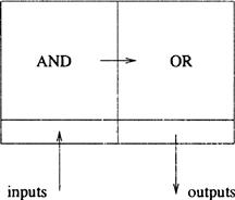
Figure 13.16 Schematic for an AND-OR array
13.4.2 ROM: Fixed AND-Programmable OR
As was seen earlier, a ROM is a read only memory device. It consists of a decoder with n inputs (or addresses) whose 2n outputs drive a memory array. As seen in Figure 13.2 a decoder can be implemented with AND gates and hence this is called the AND array. Since all possible input and output combinations exist then this is classed as a fixed array, i.e., an n input decoder requires 2n n-input AND gates to generate all product terms. As we have also seen (see Figure 10.3), the memory array is in fact a NOR array. However, the inclusion of an inverter on each column line will turn this into an OR array. Hence if the decoder has 2n outputs then the OR array must contain m OR gates with each gate having up to 2n inputs, where in this case m is the number of bits in a word. Notice that we have said “up to” 2n inputs. This is because the OR array contains the data which is programmable. The ROM architecture is thus a fixed AND-programmable OR array.
The complete circuit for a 4 × 3 bit ROM is shown in Figure 13.17(A). Note that it consists of a fixed AND structure (i.e., a 2-to-4 decoder) and a programmable OR array (i.e., a 4-to-3 encoder).The three-bit words stored in the four addresses are programmed by simply connecting each decoder output to the appropriate input of an OR gate when a logic “1” is to be stored.

Figure 13.17 A 4 × 3 bit ROM shown storing the data in the truth table
This circuit shows the ROM storing the data in the truth table of Figure 13.17(B). The Boolean equations, in fundamental sum of products form, are:
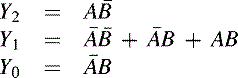
Note that rather than thinking of the ROM storing four three-bit words, an alternative view is that it is implementing a two-input, three-output truth table.
The same circuit is shown again in Figure 13.18 but this time the 2n inputs to each OR gate are shown, for simplicity, as a single input. A cross indicates a connection from the address line to the gate. The same data as in Figure 13.17 are shown stored.

Figure 13.18 A 4 × 3 bit ROM using an abbreviated notation for the OR array
As seen earlier, the physical implementation of the programmable OR array is achieved via the presence or absence of a transistor connection. This is achieved either by omitting the source or drain connections of MOS transistors or blowing fuses which are connected to the transistor terminals. Apart from using ROMs to store data or programs they can also be used to perform many digital operations, some of which are described below.
13.4.2.1 Universal Combinational Logic Function
As we have seen a ROM has all fundamental product terms available for summing and can implement an m-output, n-input truth table. This is simply achieved by connecting the address lines to the n input variables, and each output line programmed to give the appropriate output values. The advantages of such a ROM based design are: it is particularly applicable if n is large; no minimization is needed; it is cheap if mass produced; and only one IC is needed.
Example 13.7
How would the truth table shown in Figure 13.19(A) be implemented using a ROM?

Figure 13.19 Truth table used in Example 13.7 for implementation in ROM
Solution
A ROM of at least size 16 × 3 would be needed. The four address lines would be connected to the input variables A, B, C and D with the three outputs providing X, Y and Z. The required outputs (three-bit word) for each of the 16 possible input combinations would be programmed into the ROM, straight from the truth table. This is shown in Figure 13.19(B) for the first four addresses, where An and On, are the nth address line and output respectively of the ROM.
Note that because all the fundamental product terms are produced by the fixed AND array of the ROM then no minimization can take place.
13.4.2.2 Code Converter and Look-Up Table
A ROM can be used to convert an n-bit binary code (presented to the address lines) into an m-bit code (which appears at the outputs).The desired m-bit code is simply stored at the appropriate address location. Considered in this way it is a general n-to-m encoder or code converter.
Another ROM application similar to the code converter is the look-up table. Here, a ROM could be used to look up the values of, for example, a trigonometric function (e.g., sin x), by storing the values of the function in ROM. By addressing the appropriate location with a digitized version of x the value for the function stored would be output.
13.4.2.3 Sequence Generator and Waveform Generator
A ROM can be used as a sequence generator in that if the data from an n × m ROM are output, address by address, then this will generate n binary data sequences. Also, if the ROM output is passed to an m bit digital-to-analog converter (DAC) then an analog representation of the stored function will be produced. Hence a ROM with a DAC can be used as a waveform generator.
13.4.3 PAL: Programmable AND-Fixed OR
ROM provides a fixed AND-programmable OR array in which all fundamental product terms are available, thus providing a universal combinational logic solution. However, ROM is only available in limited sizes and with a restricted number of inputs. Adding an extra input means doubling the size of the ROM. Clearly a means of retaining the flexibility of the AND-OR structure while also overcoming this problem would produce a useful structure.
Virtually all combinational logic functions can be minimized to some degree, therefore allowing nonfundamental product terms to be used. Therefore, a programmable AND array would allow only the necessary product terms, after minimization, to be produced. Followed by a fixed OR array, this would allow a fixed number of product terms to be summed and so a minimized sum of products expression implemented. This type of structure is called a programmable array logic or PAL.
The structure of a hypothetical PAL is shown in Figure 13.20. This circuit has two input variables and three outputs, each of which can be composed of two product terms. The product terms are programmable via the AND array. For the connections shown the outputs are:


Figure 13.20 A programmable AND-fixed OR logic structure (i.e., PAL) with two inputs, six programmable product terms and three outputs (each summing two of the six product terms)
(Note that Y0 only has one product term so only one of the two available AND gates is used.)
Commercially available PAL part numbers are coded according to the number of inputs and outputs. For example the hypothetical PAL shown in Figure 13.20 would be coded PAL2H3, i.e., it is a PAL having two inputs and three outputs. The H indicates that the outputs are active high. One of the smallest PALs on the market is a PAL16L8 offered by Texas Instruments, AMD and several other manufacturers. This has 16 input terms and eight outputs. The L indicates that the outputs are active low. This device actually shares some of its inputs with its outputs, i.e., it has feedback. Hence, if all eight outputs are required then only eight inputs are available. The other piece of information that is required about a PAL is how many product terms each OR gate can support. This is supplied on the data sheet, and for the PAL16L8, for example, it is seven.
By adding flip-flops at the output, the designer is able to use PALs as sequential elements. The nomenclature for the device would now be PAL16R8 for example where R stands for registered output. The early PALs were fuse programmable. However, companies such as Altera, Intel and Texas Instruments added EPROM technology to these registered output PALs so that the devices could be programmed many times. These devices are called erasable programmable logic devices or EPLDs.
Very large PALs exist having gate equivalents of over 2000 gates quoted (remember a gate is defined as a two-input NAND gate). The inflexibility of only having the flip-flops at the outputs and not buried within the array (as in mask programmable ASICs) resulted in the GAL. The GAL (generic array logic) is an ultraviolet-erasable PAL with a programmable cell at each output, called an output logic macro cell (OLMC). Each OLMC contains a register and multiplexers to allow connections to and from adjacent OLMCs and from the AND/OR array. The GAL (trademark of Lattice Semiconductors) has a similar nomenclature to PALs. For example the GAL16V8 has 16 inputs and eight outputs using a versatile cell (i.e., V in the device name). However, because it uses OLMCs then it can emulate many different PAL devices in one package, having a range of inputs (up to 16) and outputs (up to eight).
Example 13.8
How could the truth table in Figure 13.19(A) be implemented using a (hypothetical) PAL with four inputs, three outputs and a total of 12 programmable product terms (i.e., four to each output)?
Solution
First, we use Karnaugh maps (Figure 13.21) to minimize the functions X, Y and Z.

Figure 13.21 Karnaugh maps for Example 13.8

The PAL, a PAL4H3, would therefore be programmed as shown in Figure 13.22.

Figure 13.22 Using a PAL to implement the truth table in Figure 13.19
13.4.4 PLA: Programmable AND-Programmable OR
The final variant of the AND-OR architectures is the programmable AND-programmable OR array or programmable logic array (PLA). With this the desired product terms can be programmed using the AND array and then as many of these terms summed together as required, via a programmable OR array, to give the desired function.
The structure of such an array with two inputs, three outputs and six programmable product terms available is shown in Figure 13.23. For the connections shown the outputs are:

Figure 13.23 A programmable AND-programmable OR logic array (i.e., PLA) with two inputs, six programmable product terms and three programmable outputs
Note that any product term can be formed by the AND gates, and that any number of these product terms can be summed by the OR gates.
Example 13.9
How would the truth table shown in Figure 13.19(A) be implemented using a (hypothetical) four-input, three-output PLA with eight product terms?
Solution
From the minimization performed to implement this truth table using the PAL in Example 13.8 it can be seen that the three Boolean expressions for X, Y and Z contain a total of nine different product terms (ACD2¯ is common to both X and Z). This PLA can only produce eight which means that product terms common to the three expressions must be found, effectively de-minimizing them to some degree.
This can be achieved by reconsidering the Karnaugh maps and not fully minimizing them, but rather looking for common implicants in the three expressions:
In this form only seven different product terms are required to implement all three functions and so the given PLA can be used as shown in Figure 13.24.
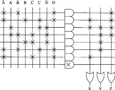
Figure 13.24 A programmable AND-programmable OR logic array (PLA) with four inputs, eight programmable product terms and three programmable outputs
13.4.5 Field-Programmable Gate Arrays
The advancement in on-chip field-programmable techniques combined with ever increasing packing densities has led to the introduction of field-programmable gate arrays or FPGAs. These devices can be considered as being the same as mask programmable gate arrays except the functionality and interconnect is programmed in the laboratory at a greatly reduced financial risk. The popularity of FPGAs is indicated by the large number of companies who currently manufacture such devices. These include Actel, Altera, AMD, Atmel, Crosspoint, Lattice, Plessey, Quicklogic, Texas Instruments, and Xilinx, to name but a few. Of these, the three that are perhaps the best known are Altera, Xilinx and Actel. In order to introduce FPGAs, some of the devices provided by these three companies will therefore be discussed. Essentially they differ in terms of: granularity; programming technique; volatility; and reprogrammability. All FPGAs consist of a versatile cell that is repeated across the chip with its size and hence cell complexity referred to as the granularity. These cells are multifunctional such that they can produce many different logic gates from a single cell. The larger the cell, the greater the complexity of gate each cell can produce. Those arrays that use a small simple cell, duplicated many times, are referred to as having fine granularity, while arrays with few, but large, complex cells are defined as coarse grain. These versatile cells have been given different names by the manufacturers, for example: modules; macrocells; and combinatorial logic blocks. The programming of the function of each cell and how each cell is interconnected is achieved via either: small fuses; onboard RAM elements that control multiplexers; or erasable programmable read only memory (EPROM) type transistors. Consequently some devices are volatile and lose their functionality when the power is removed, while others retain their functionality even with no supply connected. Finally these devices can be divided into those that can be reprogrammed many times and those that are one-time programmable.
Let us now look more closely at the FPGA types, which will be divided into: EPROM type; SRAM/MUX type; and fuse type.
13.4.5.1 EPROM Type FPGAs
The most common EPROM type FPGA device is that supplied by Altera. The range of devices available from Altera are the MAX 5000, 7000 and 9000 series (part numbers: EPM5XXX, EPM7XXX and EPM9XXX). These devices are the furthest from the true FPGAs and can be considered really as large PAL structures. They offer coarse granularity and are more an extension to Altera’s own range of electrically programmable, ultraviolet-erasable logic devices (EPLD). The versatile cell of these devices is called a macrocell. This cell is basically a PAL with a registered output. Between 16 and 256 macrocells are grouped together into an array inside another block called a logic array block (LAB) of which an FPGA can contain between 1 and 16. In addition to the macrocell array each LAB contains an I/O block and an expander which allows a larger number of product terms to be summed. Routing between the LABs is achieved via a programmable interconnect array (PIA) which has a fixed delay (3 ns worst case) that reduces the routing dependence of a design’s timing characteristics.
Since these devices are derived from EPLD technology the programming is achieved in a similar manner to an EPROM via an Altera logic programmer card in a PC connected to a master programming unit. The MAX 7000 is similar to the 5000 series except that the logic block has two more input variables. The MAX 9000 is similar to the 7000 device except that it has two levels of PIA. One is a PIA local to each LAB while the other PIA connects all LABs together. Both the 7000 and 9000 series are E2PROM devices and hence do not need an ultraviolet source to be erased.
It should be noted though that these devices are not true FPGAs and have a limited number of flip-flops available (one per macrocell). Hence, the Altera Max 5000/7000/9000 series is more suited to combinatorially intensive circuits. For more register intensive designs Altera offers the Flex 8000 and 10 K series of FPGAs which uses an SRAM memory cell based programming technique (as used by Xilinx—see next section); although currently rather expensive it will in time become an attractive economical option. The Flex 8000 series (part number: EPF8XXX) has gate counts from 2000 to 16000 gates. The 10 K series (part number: EPF10XXX) however, has gate counts from 10000 to 100000 gates!
13.4.5.2 SRAM/MUX Type FPGAs
The most common FPGA that uses the SRAM/MUX programming environment is that supplied by Xilinx. The range of devices provided by Xilinx consists of the XC2000, XC3000 and XC4000. The versatile cell of these devices is the “configurable logic block” (CLB) with each FPGA consisting of an array of these surrounded by a periphery of I/O blocks. Each CLB contains combinational logic, registers and multiplexers and so, like the Altera devices, has a relatively coarse granularity. The Xilinx devices are programmed via the contents of an on-board static RAM array which gives these FPGAs the capability of being reprogrammed (even while in operation). However, the volatility of SRAM memory cells requires the circuit configuration to be held in an EPROM alongside the Xilinx FPGA.
A recent addition to the Xilinx family is the XC6000 range. This family has the same reprogrammability nature as the other devices except it is possible to partially reconfigure these devices. This opens up the potential for fast in-circuit reprogramming of small parts of the device for learning applications such as neural networks.
13.4.5.3 Fuse Type FPGAs
The most common fuse type FPGA is that supplied by Actel. These devices are divided into the Act1, Act2 and Act3 families. The Act1 FPGAs (part numbers: AI0XX) contain two programmable cells: “Actmod” and “IOmod.” The versatile core cell is the Actmod which is simply based around a 4-to-1 multiplexer for Act 1. This versatile cell is shown in Figure 13.25. Since this cell is relatively small the array is classed as fine grain. By tying the inputs to either a logic “0” or logic “1” this versatile cell can perform 722 different digital functions. The programmable IOmod cell is used to connect the logic created from the Actmods to the outside world. This cell can be configured as various types of inputs and/or outputs (bidirectional, tristate, CMOS, TTL, etc.). Unlike the Xilinx and Altera devices, the Actel range are programmed using fuse technology with desired connections simply blown (strictly called an antifuse). These devices are therefore “one time programmable” (OTP) and cannot be reprogrammed. The arrays have an architecture similar to a channelled gate array with the repeating cell (Actmod) arranged in rows with routing between each row. The routing contains horizontal and vertical metal wires with antifuses at the intersection points.

Figure 13.25 Versatile cell used for Actel Act1 range of fused FPGAs
Other devices in the Actel range are the Act2 (part numbers: A12XX) and the Act3 (part numbers: A14XX) devices. These use two repeating cells in the array. The first is a more complex Actmod cell called Cmod, used for combinational purposes, while the other cell is a Cmod with a flip-flop.
Table 13.1 shows a comparison of some of the FPGA devices offered by Altera, Xilinx, and Actel.
Table 13.1 Comparison of some FPGA types

Example 13.10
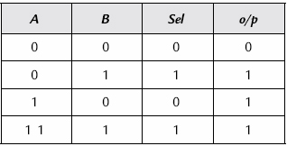
Consider the versatile Actel cell shown in Figure 13.25. What functions are produced if the following signals are applied to its inputs:
Assume that the signals A and B are inputs having values of “0” or “1” and that for each multiplexer when the select line is low the lower input is selected.
Solution
(a) In this case the OR gate output is always zero and so the lower line is selected. This is derived from the lower multiplexer whose select line is controlled by the only input “A”. With the inputs to this multiplexer at “0” for the upper line and “1” for the lower line, the output follows that of an inverter.
(b) Here it is helpful to construct a truth table and include in this table the output of the OR gate, called sel (See Table 13.2). We can thus see that the function is a two-input OR gate.
Table 13.2 Truth table for Example 13.10(b)
(c) Again a truth table (including sel) is useful to work out the function implemented (See Table 13.3).
Table 13.3 Truth table for Example 13.10(c)

A Karnaugh map for the output is shown in Table 13.4, which generates the function:
![]()
Table 13.4 Karnaugh map for Example 13.10(c) output

13.4.6 CAD Tools for Field-Programmable Logic
The programming of field-programmable logic devices is implemented directly via a computer. The software needed for PALs and PLAs is usually a simple matter of producing a programming file called a fuse or an EPROM bit file. This file has a standard format (called JEDEC) and contains a list of l’s and 0’s. This file is automatically generated from either Boolean equations, truth tables or state diagrams using programs such as ABEL (DataIO Corp.), PALASM (AMD Inc.) and CUPL (Logical Devices Inc.). In other words the minimization is done for you and it is not necessary to draw out any Karnaugh maps. Software programs that can directly convert a schematic representation into a JEDEC file are also available. Since these devices have only an MSI complexity level, the software tools are relatively simple to use and also inexpensive.
The FPGAs, on the other hand, have capacities of LSI and VLSI level and are much more complex. Since FPGAs are similar in nature to mask programmable gate arrays, the associated CAD tools have been derived from mask programmable ASICs and follow that of Figure 13.13; that is: schematic capture (or VHDL), prelayout simulation, layout, back annotation and postlayout simulation.
It should be noted that FPGA simulation philosophy is somewhat different from mask programmable gate arrays. With mask programmable devices, 100% simulation is absolutely essential since these circuits cannot be rectified after fabrication without incurring large financial and time penalties. These penalties are virtually eliminated with FPGA technology due to the fast programming time in the laboratory and the low cost of devices. For one-time programmable devices (such as Actel) the penalty is the price of one chip while for erasable devices (such as Xilinx) the devices can simply be reprogrammed. Hence, the pressure to simulate 100% is not as great.
For those devices that are reprogrammable, this results in an inexpensive iterative procedure whereby a device is programmed and then tested in the final system. If the device fails it can be reprogrammed with the fault corrected. For OTP type FPGAs then a new device will have to be blown at each iteration; although it will incur a small charge the cost is considerably less than mask programmable arrays. It is not uncommon for FPGA designs (both reprogrammable and OTP) to experience four iterations before a working device is obtained. This is totally unthinkable for mask programmable designs where a “right first time approach” has to be employed—hence, the reliance on the simulator.
Since fuses, SRAM/MUX cells, etc., are used to control the connectivity, the delays caused by these elements must be added to the wire delays for postlayout simulation. Hence it is for this reason that FPGAs operate at a lower frequency than mask programmable gate arrays. The large delays in the routing path also mean that timing characteristics are routing dependent. Hence, changing the placement positions of core cells (by altering the pin out for example) will result in a different timing performance. If the design is synchronous then this should not be a problem with the exception of the shift register problem referred to in Figure. 13.14. It should also be noted that the prelayout simulation of FPGAs on some occasions is only a unit delay (i.e., 1 ns for all gates) or functional simulation. It does not take into account fan-out, individual gate delays, set-up and hold time, minimum clock pulse widths (i.e., spike and glitch detector), etc., and does not make any estimate of the wire delay. Hence the simulation at this stage is not reflective of how the final design will perform. To obtain the true delays, the FPGA must be laid out and the delays back annotated for a postlayout simulation. This will provide an accurate simulation and hence reveal any design errors. Unfortunately, if a mistake is found then the designer must return all the way back to the original schematic. The design must again be prelayout simulated, laid out and delays back annotated before the postlayout simulation can be repeated. This tedious iterative procedure is another reason why FPGAs are usually programmed prematurely with a limited simulation. It should be mentioned that an FPGA is sometimes used as a prototyping route prior to migrating to a mask programmable ASIC. Hence the practice of postlayout simulation using back annotated delays is an important discipline for an engineer to learn in preparation for moving to mask programmable ASICs.
When all the CAD stages are completed the FPGA netlist file is converted into a programming file to program the device. This is either a standard EPROM bit file for the Xilinx and Altera arrays or a fuse file for the Actel devices. Once a device is programmed, debug and diagnostic facilities are available. These allow the logic state of any node in the circuit to be investigated after a series of signals has been passed to the chip via the PC serial or parallel port. This feature is unique to FPGAs since each node is addressable, unlike mask programmable devices.
FPGA CAD tools are usually divided into two parts. The first is the prelayout stage or front-end software, i.e., schematic and prelayout simulation. The CAD tools here are generic (suitable for any FPGA) and are provided by proprietary packages such as Mentor Graphics, Cadence, Viewlogic, Orcad, etc. However, to access the FPGAs the corresponding libraries are required for schematic symbols and models.
The second part is called the back-end software incorporating: layout; back annotation of routing delays; programming file generation and debug. The software for this part is usually tied to a particular type of FPGA and is supplied by the FPGA manufacturer.
For example consider a typical CAD route with Actel on a PC. The prelayout (or front end) tools supplied by Viewlogic can be used to draw the schematic using a package called Viewdraw and the prelayout functional simulation is performed with Viewsim. In both cases library files are needed for the desired FPGA. Once the design is correct it can be converted into an Actel net-list using a netlist translator. This new file is then passed into the CAD tools supplied by Actel (called Actel Logic System – ALS) ready for place and routing. The parasitic delays can be extracted and back annotated out of ALS back into Viewlogic so that a post-layout simulation can be performed again with Viewsim. If the simulation is not correct then the circuit schematic must be modified and the array is placed and routed again. Actel provides a static timer to check set-up and hold time and calculate the delays down all wires, indicating which wire is the heaviest loaded. A useful facility is the net criticality assignment which allows nets to be tagged depending on how speed critical they are. This facility controls the placing and routing of the logic in order to minimize wiring delays wherever possible. The device is finally programmed by first creating a fuse file and then blowing the fuses via a piece of hardware called an activator. This connects to an Actel programming card inside the PC. As an example of the length of time the place and route software can take to complete, the authors ran a design for a 68-pin Actel 1020 device. The layout process took approximately 10 minutes using a 486, 66 MHz PC and utilized 514 (approximately 1200 gates) of the 547 modules available (i.e., a utilization of 94%). In addition, on the same computer the fuse programming via the activator took around 1 minute to complete its program. With mask programmable ASICs, however, the programming step can take at least four weeks to complete! This is one of the great advantages that FPGAs have over mask programmable ASICs. Note, however, that as with mask programmable arrays the FPGA manufacturers only provide a limited range of array sizes. The final design thus never ever uses all of the gates available and hence silicon is wasted. Also, as the gates are used up on the array, the ability for the router to access the remaining gates decreases and hence, although a manufacturer may quote a maximum gate count for the array, the important figure is the percentage utilization.
Actel FPGAs also have comprehensive post-programming test facilities available under the option “Debug.” These consist of: the functional debug option; and the in-circuit diagnostic tool. The functional debug test involves sending test vectors from the PC to the activator, which houses the FPGA during programming, and simple tests can be carried out. The in-circuit diagnostic tool is used to check the real time operation of the device when in the final PCB. This test is 100% observable in that any node within the chip can be monitored in real time with an oscilloscope via two dedicated pins on the FPGA.
The Xilinx FPGA devices are programmed in a similar way by using two pieces of software. Again, typical front-end software for these devices is Viewlogic utilizing Viewdraw and Viewsim for circuit entry and functional simulation, respectively. The netlist for the schematic is this time converted into a Xilinx netlist and the design can now move into the Xilinx development software supplied by Xilinx (called XACT). Although individual programs exist for place and route, parasitic extract, programming file generation, etc., Xilinx provides a simple to use compilation utility called XMAKE. This runs all of these steps in one process. Parasitic delays can again be back annotated to Viewsim for a timing simulation with parasitics included. A static timing analyzer is again available so that the effects of delays can be observed on set-up and hold time without having to apply input stimuli. Bit stream configuration data, used in conjunction with a Xilinx provided cable, allow the data to be downloaded to the chip for configuration. As with Actel, both debug and diagnostic software exist such that the device can be tested and any node in the circuit monitored in real time. The bit stream data can be converted into either Intel (MCS-86), Motorola (EXORMAX) or Tektronix (TEKHEX) PROM file formats for subsequent PROM or EPROM programming. The one disadvantage of these devices as compared to the Actel devices is that when in final use the device needs to have an associated PROM or EPROM, which increases the component count.
13.5 VHDL
As systems become more complex, the use of schematic capture programs to specify the design becomes unmanageable. For designs above 10,000 gates, an alternative design entry technique of behavioral specification is invariably employed. This is a high-level programming language that is textual in nature, describes behavior and maps to hardware. The most commonly accepted behavioral language is that standardized by the IEEE (standard 1076) in 1987 called VHDL. VHDL is an acronym for VHSIC Hardware Description Language where VHSIC (Very High Scale Integrated Circuits) is the next level of integration above VLSI. This language was developed by the USA Department of Defense and is now a worldwide standard for describing general digital hardware. The language allows a system to be described at many different levels from the lowest level of logic gates (called structural) through to behavioral level. At behavioral level the design is represented in terms of programming statements which makes no use of logic gates. This behavior can use a digital (i.e., Boolean), integer or real representation of the circuit operation. A system designer can specify the design at a high level (i.e., in integer behavioral) and then pass this source code to another member of the group to break the design down into individual smaller blocks (partitioning). A block in behavioral form requires only a few lines of code and hence is not as complex as a structural logic gate description and hence has a shorter simulation time. Since the code supports mixed levels (i.e., gate and behavior) then the system can be represented with some blocks represented at the gate level and the rest at behavioral. Thus the complete system can be simulated in a much shorter time.
One of the biggest problems of designing an ASIC is the interpretation of the specification required by the customer. Because VHDL has a high-level description capability it can be used also as a formal specification language and establishes a common communication between contractors or within a group. Another problem of ASIC design is that you have to choose a foundry before a design is started, thus committing you to that manufacturer. Hence, it is usual to insist on second sourcing outlets to avoid production hold-ups. However, VHDL at the high level is technology and process independent and is therefore transportable into other processes and CAD tools. It is not surprising that many companies are now insisting on a VHDL description for their system as an extra deliverable as well as the chip itself.
A simple example of a VHDL behavioral code for a 2-to-1 multiplexer is shown in Table 13.5. This source code is divided into two parts: entity and architecture. The entity lists the input and output pins and what form they are—bit or binary in this case—while the architecture describes the behavior of the multiplexer. The process labeled f1 is only run if any of the inputs d0, d1 or sel change, i.e., it is an event driven simulator. If one of these events occurs, the IF statement is processed and the output q is set depending upon the value of sel.
Table 13.5 VHDL behavioral code for a 2-to-1 multiplexer
Notice that since this is a behavioral description then no logic gates are used in the architecture. The next stage would be to convert this design into logic gates. This can be performed in two ways: automatically or manually. With the automatic approach an additional CAD software package is required called a synthesizer. These are available at an extra charge and will generate the logic gates required to implement the desired behavior. Alternatively this step can be performed manually. A typical VHDL structural description of the above multiplexer implemented with logic gates is shown in Table 13.6.
Table 13.6 VHDL structure code for a 2-to-1 multiplexer
Since this is only a trivial example, a manual synthesis is possible. It is also apparent that a behavioral code is more succinct than a structural one hence the simulation is faster. As the design becomes more complex then the use of an automatic synthesizer is essential.
13.6 Choosing a Design Route
So we now know all the options available to a digital circuit designer. The decision is now to choose the appropriate route. It is wise at this point to revisit the ten questions that were raised at the beginning of this chapter and to consider them in the light of the summarized information given in Table 13.7.
Table 13.7 Comparison of digital design routes

A standard part (called Std. Part in the table) design route (i.e., 74HCT, etc.) is certainly the quickest to get started and can handle large and complex designs. However, it may well be limited when the design needs to be miniaturized or put into production. Also design techniques with standard products often tend to be ad hoc and in some instances not synchronous. The design may use RC components, 555 timers and gated clocks. If the design is only a one-off and it functions correctly then this will be perfectly satisfactory if size and power are not an issue. However, if the design requires miniaturization or transfer to an ASIC for power consumption reasons, then the circuit will have to be redesigned for a totally synchronous approach.
Of the AND-OR array devices a ROM device can be used to efficiently perform a number of digital tasks, while PALs and PLAs are also widely available, providing much of the capability of ROM but with smaller circuits. However, it is necessary to minimize the Boolean functions before they can be implemented in a PAL or PLA. A PAL allows a fixed number of minimized product terms to be summed, while a PLA enables any number of the product terms formed to be summed. However, although PALs and PLAs are quite adequate for gate counts of the order of 500, they are limited due to having no buried registers.
Obviously, no one route will satisfy all options but FPGAs are becoming a strong prototyping contender. At present, FPGA performance is still below that of mask programmable gate arrays (MPGA) which still have the edge in terms of high performance (high speed, low power consumption), high gate density or large volumes. However, for small volumes, FPGAs offer a virtually immediate turn around time and relatively low cost (particularly in terms of the nonrecurring engineering (NRE) costs, which can be very large for many ASIC designs). In addition, since a single FPGA is relatively inexpensive the risk factor is significantly less and hence, the emphasis on the simulation stage is reduced. An FPGA can thus be programmed and tested rapidly. However, if a design fault exists then the fault can be quickly corrected and the device reprogrammed. The use of an FPGA is a very powerful vehicle for testing out an idea before going to volume production. Translators are available which can convert FPGA designs into mask programmable ASICs once the design is confirmed at the prototype stage. FPGAs also/support VHDL description and since VHDL is transportable it can be transferred into standard cell (SC) options if sufficient volume is expected.
1 This decoder has outputs that are active low; however, for this application we shall assume that the outputs are active high.
2 In some environments a separate static timing analyzer is available. This checks all timing delays around bistables with regard to clock and data and confirms that no set-up and hold time violations are present. This removes the time-consuming process of writing a stimulus file for the timing simulator that covers all possible combinations of inputs around all bistables.