
Chapter 2
The Semiconductor Diode
The semiconductor diode, like its predecessor the thermionic diode, conducts current in one direction only. It is arguable that diodes in general are not really active devices at all, but simply nonlinear passive devices. The earliest semiconductor diode was a point contact device and was already in use before the First World War, being quite possibly contemporary with the earliest thermionic diodes. It consisted of a sharp pointed piece of springy wire (the “cat’s whisker”) pressed against a lump of mineral (the “crystal”), usually Galena, an ore containing sulfide of lead. The crystal detector was widely employed as the detector in the crystal sets that were popular in the early days of broadcasting. Given a long aerial and a good earth, the crystal set produced an adequate output for use with sensitive headphones, while with so few stations on the air in those days the limited selectivity of the crystal set was not too serious a problem. The crystal and cat’s whisker variety of point contact diode was a very hit and miss affair, with the listener probing the surface of the crystal to find a good spot. Later, new techniques and materials were developed, enabling robust preadjusted point contact diodes useful at microwave frequencies to be produced. These were used in radar sets such as AI Mk.10, an airborne interceptor radar that was in service during (and long after!) the Second World War. Germanium point contact diodes are still manufactured and are useful where a diode with a low forward voltage drop at modest current (a milliampere or so) combined with very low reverse capacitance is required. However, for the last twenty years silicon has predominated as the preferred semiconductor material for both diode and transistor manufacture, while point contact construction gave way to junction technology even earlier.
Figure 2.1A shows the I/V characteristics of practical diodes. Silicon diodes are manufactured hundreds or thousands at a time, commencing with a thin wafer of single crystal silicon several inches in diameter, which is later scribed and separated to obtain the individual diodes. Silicon is one of those substances that crystallize in a cubic lattice structure; another is sodium chloride—common salt—but that is a compound, not an element like silicon. Silicon, in the form of silicon dioxide, is one of the most abundant elements in the carth’s crust, occurring as quartz, in sandstone, etc. When reduced to elementary silicon, purified and grown from the melt as a single crystal, it is called intrinsic silicon and is a poor conductor of electricity, at least at room temperature. However, if a few of the silicon atoms in the atomic lattice are replaced with atoms of the pentavalent element phosphorus, (which has five valence electrons in its outer shell, unlike quadravalent silicon that has four outer electrons), then there are electrons “going begging,” with no corresponding electron in a neighboring atom with which to form a bond pair. These spare electrons can move around in the semiconductor lattice, rather like the electrons in a metallic conductor. The higher the doping level, the more free electrons and the higher the conductivity of the silicon, which is described as n-type. This simply indicates that the current flow is by means of negative charge carriers, i.e., electrons. p-type silicon is obtained by doping the monocrystalline lattice with a sprinkling of trivalent atoms, such as boron. Where one of these is substituted in the lattice next to a silicon atom, the latter has one of its electrons “unpaired,” a state of affairs described as a hole. If this is filled by an electron from a silicon atom to the right, then while that electron has moved to the left, the hole has effectively moved to the right. It turns out that the spare electrons in n-type silicon are more mobile than the holes in p-type, which explains why very high-frequency transistors are more easy to produce in NPN than PNP types—but that is jumping ahead.
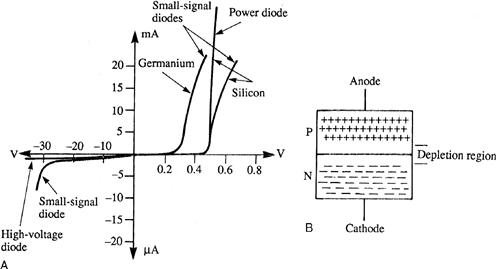
Figure 2.1 Semiconductor diodes. (A) I/V characteristics; (B) Diagrammatic representation of PN diode, showing majority carriers and depletion region.
To return to the silicon junction diode: the construction of this is as in Figure 2.1B, which indicates the lack of carriers (called a depletion region) in the immediate neighborhood of the junction. Here, the electrons from the N region have been attracted across to the P region to fill holes. This disturbance of the charge pattern that one would expect to find throughout n-type and p-type material represents a potential barrier, which prevents further migration of carriers across the junction. When the diode is reverse biased, the depletion region simply becomes more extensive.
The associated redistribution of charge represents a transient charging current, so that a reversed biased diode is inherently capacitive. If a forward bias voltage large enough to overcome the potential barrier is applied to the junction, about 0.6V in silicon, then current will flow; in the case of a large-area power diode, even a current of several amperes will only result in a small further increase in the voltage drop across the diode, as indicated in Figure 2.1A. The incremental or slope resistance rd of a forward biased diode at room temperature is given approximately by 25/Ia ohms, where the current through the diode Ia is in milliamperes. Hence the incremental resistance at 10 μA is 2K5, at 100 μA is 250R, and so on, but it bottoms out at a few ohms at high currents, where the bulk resistance of the semiconductor material and the resistance of the leads and bonding pads, etc., come to predominate. This figure would apply to a small-signal diode: the minimum slope resistance of a high-current rectifier diode would be in the milliohm region.
Power diodes are used in power supply rectifier circuits and similar applications, while small signal diodes are widely used as detectors in radio-frequency circuits and for general purpose signal processing, as will appear in later chapters. Also worth mentioning are special purpose small-signal diodes such as the tunnel diode, backward diode, varactor diode, PIN diode, snap-off diode, Zener diode and Schottky diode; the last of these is also used as a rectifier in power circuits. However, the tunnel diode and its degenerate cousin the backward diode are only used in a few very specialized applications nowadays.
The varactor diode or varicap is a diode designed solely for reverse biased use. A special doping profile giving an abrupt or “hyperabrupt” junction is used. This results in a diode whose reverse capacitance varies widely according to the magnitude of the reverse bias. The capacitance is specified at two voltages, e.g., 1V and 15V, and may provide a capacitance ratio of 2:1 or 3:1 for types intended for use at UHF, up to 30:1 for types designed for tuning in AM radio sets. In these applications the peak-to-peak amplitude of the RF voltage applied to the diode is small compared with the reverse bias voltage, even at minimum bias (where the capacitance is maximum). So the varactor behaves like a normal mechanical air-spaced tuning capacitor except that it is adjusted by a DC voltage rather than a rotary shaft. Tuning varactors are designed to have a low series loss rs so that they exhibit a high quality factor Q, defined as Xc/rs, over the range of frequencies for that they are designed.
Another use for varactors is as frequency multipliers. If an RF voltage with a peak-to-peak amplitude of several volts is applied to a reverse biased diode, its capacitance will vary in sympathy with the RF voltage. Thus, the device is behaving as a nonlinear (voltage dependent) capacitor, and as a result the RF current will contain harmonic components that can be extracted by suitable filtering.
The p-type/intrinsic/n-type diode or PIN diode is a p-n junction diode, but fabricated so as to have a third region of intrinsic (undoped) silicon between the P and N regions. When forward biased by a direct current it can pass radio-frequency signals without distortion, down to some minimum frequency set by the lifetime of the current carriers—holes or electrons—in the intrinsic region. As the forward current is reduced, the resistance to the flow of the RF signal increases, but it does not vary over an individual cycle of the RF current. As the direct current is reduced to zero, the resistance rises toward infinity; when the diode is reverse biased, only a very small amount of RF current can flow, via the diode’s reverse biased capacitance. The construction ensures that this is very small, so the PIN diode can be used as an electronically controlled RF switch or relay, on when forward biased and off when reverse biased. It can also be used as a variable resistor or attenuator by adjusting the amount of forward current. An ordinary p-n diode can also be used as an RF switch, but it is necessary to ensure that the peak RF current when “on” is much smaller than the direct current, otherwise waveform distortion will occur. It is the long lifetime of carriers in the intrinsic region (long compared with a single cycle of the RF), which enables the PIN diode to operate as an adjustable linear resistor, even when the peaks of the RF current exceed the direct current.
When a PN junction diode that has been carrying current in the forward direction is suddenly reverse biased, the current does not cease instantaneously. The charge has first to redistribute itself to re-establish the depletion layer. Thus for a very brief period, the reverse current flow is much greater than the small steady-state reverse leakage current. The more rapidly the diode is reverse biased, the larger the transient current and the more rapidly the charge is extracted. Snap-off diodes are designed so that the end of the reverse current recovery pulse is very abrupt, rather than the tailing off observed in ordinary PN junction diodes. It is thus possible to produce a very short sharp current pulse by rapidly reverse biasing a snap-off diode. This can be used for a number of applications, such as high-order harmonic generation (turning a VHF or UHF drive current into a microwave signal) or operating the sampling gate in a digital sampling oscilloscope.
Small-signal Schottky diodes operate by a fundamentally different form of forward conduction. As a result of this, there is virtually no stored charge to be recovered when they are reverse biased, enabling them to operate efficiently as detectors or rectifiers at very high frequencies. Zener diodes conduct in the forward direction like any other silicon diode, but they also conduct in the reverse direction, and this is how they are normally used. At low reverse voltages, a Zener diode conducts only a very small leakage current like any other diode. But when the voltage reaches the nominal Zener voltage, the diode current increases rapidly, exhibiting a low incremental resistance. Diodes with a low breakdown voltage, up to about 4V, operate in true Zener breakdown: this conduction mechanism exhibits a small negative temperature coefficient of voltage. Higher-voltage diodes, rated at 6V and up, operate by a different mechanism called avalanche breakdown, which exhibits a small positive temperature coefficient. In diodes rated at about 5V both mechanisms occur, resulting in a very low or zero temperature coefficient of voltage. However, the lowest slope resistance occurs in diodes of about 7V breakdown voltage.
Reference
1. EDN. Harold P, ed. Current-feedback op-amps ease high-speed circuit design, 1988.