
Chapter 33
Microprocessor and Microcontroller Overview
Many of today’s complex electronic systems are based on the use of a microprocessor or microcontroller. Such systems comprise hardware that is controlled by software. If it is necessary to change the way that the system behaves it is the software (rather than the hardware) that is changed.
In this chapter we provide an introduction to microprocessors and explain, in simple terms, both how they operate and how they are used. We shall start by explaining some of the terminology that is used to describe different types of system that involve the use of a microprocessor or a similar device.
33.1 Microprocessor Systems
Microprocessor systems are usually assembled on a single PCB comprising a microprocessor CPU together with a number of specialized support chips. These very large scale integrated (VLSI) devices provide input and output to the system, control and timing as well as storage for programs and data.
Typical applications for microprocessor systems include the control of complex industrial processes. Typical examples are based on families of chips such as the Z80CPU plus Z80PIO, Z80CTC, and Z80SIO.
33.2 Single-Chip Microcomputers
A single-chip microcomputer is a complete computer system (comprising CPU, RAM and ROM etc.) in a single VLSI package. A single-chip microcomputer requires very little external circuitry in order to provide all of the functions associated with a complete computer system (but usually with limited input and output capability).
Single-chip microcomputers may be programmed using in-built programmable memories or via external memory chips. Typical applications of single-chip microcomputers include computer printers, instrument controllers, and displays. A typical example is the Z84C.
33.3 Microcontrollers
A microcontroller is a single-chip microcomputer that is designed specifically for control rather than general-purpose applications. They are often used to satisfy a particular control requirement, such as controlling a motor drive. Single-chip microcomputers, on the other hand, usually perform a variety of different functions and may control several processes at the same time.
Typical applications include control of peripheral devices such as motors, drives,printers, and minor subsystem components. Typical examples are the Z86E, 8051, 68705 and 89C51.
33.4 Microprocessor systems
The basic components of any microprocessor system (see Figure 33.1) are:
(a) a central processing unit (CPU);
(b) a memory, comprising both ‘read/write’ and ‘read only’ devices (commonly called RAM and ROM, respectively);
(c) a means of providing input and output (I/O). For example, a keypad for input and a display for output.
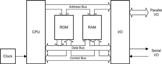
Figure 33.1 Block diagram of a microprocessor system
In a microprocessor system the functions of the CPU are provided by a single very large scale integrated (VLSI) microprocessor chip (see Figure 33.2). This chip is equivalent to many thousands of individual transistors. Semiconductor devices are also used to provide the read/write and read-only memory. Strictly speaking, both types of memory permit “random access” since any item of data can be retrieved with equal ease regardless of its actual location within the memory. Despite this, the term RAM has become synonymous with semiconductor read/write memory.

Figure 33.2 A Z80 microprocessor
The basic components of the system (CPU, RAM, ROM, and I/O) are linked together using a multiple-wire connecting system known as a bus (see Figure 33.1). Three different buses are present, these are:
(a) the address bus used to specify memory locations;
(b) the data bus on which data is transferred between devices; and
(c) the control bus which provides timing and control signals throughout the system.
The number of individual lines present within the address bus and data bus depends upon the particular microprocessor employed. Signals on all lines, no matter whether they are used for address, data, or control, can exist in only two basic states: logic 0 (low) or logic 1 (high). Data and addresses are represented by binary numbers (a sequence of 1s and 0s) that appear respectively on the data and address bus.
Many microprocessors designed for control and instrumentation applications make use of an 8-bit data bus and a 16-bit address bus. Others have data and address buses which can operate with as many as 128 bits at a time.
The largest binary number that can appear on an 8-bit data bus corresponds to the condition when all eight lines are at logic 1. Therefore the largest value of data that can be present on the bus at any instant of time is equivalent to the binary number 11111111 (or 255). Similarly, the highest address that can appear on a 16-bit address bus is 1111111111111111 (or 65,535). The full range of data values and addresses for a simple microprocessor of this type is thus:
| Data | from | 00000000 |
| to | 11111111 | |
| Addresses | from | 0000000000000000 |
| to | 1111111111111111 |
33.4.1 Data Representation
Binary numbers—particularly large ones—are not very convenient. To make numbers easier to handle we often convert binary numbers to hexadecimal (base 16). This format is easier for mere humans to comprehend and offers the advantage over denary (base 10) in that it can be converted to and from binary with ease. The first sixteen numbers in binary, denary, and hexadecimal are shown in the table below. A single hexadecimal character (in the range zero to F) is used to represent a group of four binary digits (bits). This group of four bits (or single hex character) is sometimes called a nibble.
A byte of data comprises a group of eight bits. Thus a byte can be represented by just two hexadecimal (hex) characters. A group of sixteen bits (a word) can be represented by four hex characters, thirty-two bits (a double word by eight hex characters, and so on).
The value of a byte expressed in binary can be easily converted to hex by arranging the bits in groups of four and converting each nibble into hexadecimal using Table 33.1.
Table 33.1 Binary, denary and hexadecimal
| Binary (base 2) | Denary (base 10) | Hexadecimal (base 16) |
| 0000 | 0 | 0 |
| 0001 | 1 | 1 |
| 0010 | 2 | 2 |
| 0011 | 3 | 3 |
| 0100 | 4 | 4 |
| 0101 | 5 | 5 |
| 0110 | 6 | 6 |
| 0111 | 7 | 7 |
| 1000 | 8 | 8 |
| 1001 | 9 | 9 |
| 1010 | 10 | A |
| 1011 | 11 | B |
| 1100 | 12 | C |
| 1101 | 13 | D |
| 1110 | 14 | E |
| 1111 | 15 | F |
Note that, to avoid confusion about whether a number is hexadecimal or decimal, we often place a symbol before a hexadecimal number or add an H to the end of the number. For example, 64 means decimal “sixty-four”; whereas, $64 means hexadecimal “six-four”, which is equivalent to decimal 100. Similarly, 7FH means hexadecimal “seven-F” which is equivalent to decimal 127.
Solution
From Table 33.1, A = 1010 and 3 = 0101. Thus, A3 in hexadecimal is equivalent to 10100101 in binary.
Example 33.2
Convert binary 11101000 binary to hexadecimal.
Solution
From Table 33.1, 1110 = E and 1000 = 8. Thus, 11101000 in binary is equivalent to E8 in hexadecimal.
33.5 Data Types
A byte of data can be stored at each address within the total memory space of a microprocessor system. Hence, one byte can be stored at each of the 65,536 memory locations within a microprocessor system having a 16-bit address bus.
Individual bits within a byte are numbered from 0 (least significant bit) to 7 (most significant bit). In the case of 16-bit words, the bits are numbered from 0 (least significant bit) to 15 (most significant bit).
Negative (or signed) numbers can be represented using two’s complement notation where the leading (most significant) bit indicates the sign of the number (1 = negative, 0 = positive). For example, the signed 8-bit number 10000001 represents the denary number −1.
The range of integer data values that can be represented as bytes, words and long words are shown in Table 33.2.
Table 33.2 Data types
| Data type | Bits | Range of values |
| Unsigned byte | 8 | 0 to 255 |
| Signed byte | 8 | −128 to +127 |
| Unsigned word | 16 | 0 to 65,535 |
| Signed word | 16 | −32,768 to +32,767 |
33.6 Data Storage
The semiconductor ROM within a microprocessor system provides storage for the program code as well as any permanent data that requires storage. All of this data is referred to as nonvolatile because it remains intact when the power supply is disconnected.
The semiconductor RAM within a microprocessor system provides storage for the transient data and variables that are used by programs. Part of the RAM is also be used by the microprocessor as a temporary store for data while carrying out its normal processing tasks.
It is important to note that any program or data stored in RAM will be lost when the power supply is switched off or disconnected. The only exception to this is CMOS RAM that is kept alive by means of a small battery. This battery-backed memory is used to retain important data, such as the time and date.
When expressing the amount of storage provided by a memory device we usually use kilobytes (Kbyte). It is important to note that a kilobyte of memory is actually 1,024 bytes (not 1,000 bytes). The reason for choosing the Kbyte rather than the kbyte (1,000 bytes) is that 1,024 happens to be the nearest power of 2 (note that 210= 1,024).
The capacity of a semiconductor ROM is usually specified in terms of an address range and the number of bits stored at each address. For example, 2K × 8 bits (capacity 2 Kbytes), 4K × 8 bits (capacity 4 Kbytes), and so on. Note that it is not always necessary (or desirable) for the entire memory space of a microprocessor to be populated by memory devices.
33.7 The Microprocessor
The microprocessor central processing unit (CPU) forms the heart of any microprocessor or microcomputer system computer and, consequently, its operation is crucial to the entire system.
The primary function of the microprocessor is that of fetching, decoding, and executing instructions resident in memory. As such, it must be able to transfer data from external memory into its own internal registers and vice versa. Furthermore, it must operate predictably, distinguishing, for example, between an operation contained within an instruction and any accompanying addresses of read/write memory locations. In addition, various system housekeeping tasks need to be performed including being able to suspend normal processing in order to respond to an external device that needs attention.
The main parts of a microprocessor CPU are:
(a) registers for temporary storage of addresses and data;
(b) an arithmetic logic unit (ALU) that performs arithmetic and logic operations;
(c) a unit that receives and decodes instructions; and
(d) a means of controlling and timing operations within the system.
Figure 33.3 shows the principal internal features of a typical 8-bit microprocessor. We will briefly explain each of these features in turn.
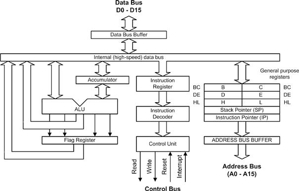
Figure 33.3 Internal architecture of a typical 8-bit microprocessor CPU
33.7.1 Accumulator
The accumulator functions as a source and destination register for many of the basic microprocessor operations. As a source register it contains the data that will be used in a particular operation while as a destination register it will be used to hold the result of a particular operation. The accumulator (or A-register) features in a very large number of microprocessor operations, consequently more reference is made to this register than any others.
33.7.2 Instruction Register
The instruction register provides a temporary storage location in which the current microprocessor instruction is held while it is being decoded. Program instructions are passed into the microprocessor, one at time, through the data bus.
On the first part of each machine cycle, the instruction is fetched and decoded. The instruction is executed on the second (and subsequent) machine cycles. Each machine cycle takes a finite time (usually less than a microsecond) depending upon the frequency of the microprocessor’s clock.
33.7.3 Data Bus (D0 to D7)
The external data bus provides a highway for data that links all of the system components (such as random access memory, read-only memory, and input/output devices) together. In an 8-bit system, the data bus has eight data lines, labeled D0 (the least significant bit) to D7 (the most significant bit) and data is moved around in groups of eight bits, or bytes. With a sixteen bit data bus the data lines are labeled D0 to D15, and so on.
33.7.4 Data Bus Buffer
The data bus buffer is a temporary register through which bytes of data pass on their way into, and out of, the microprocessor. The buffer is thus referred to as bidirectional with data passing out of the microprocessor on a write operation and into the processor during a read operation. The direction of data transfer is determined by the control unit as it responds to each individual program instruction.
33.7.5 Internal Data Bus
The internal data bus is a high-speed data highway that links all of the microprocessor’s internal elements together. Data is constantly flowing backward and forward along the internal data bus lines.
33.7.6 General-Purpose Registers
Many microprocessor operations (for example, adding two 8-bit numbers together) require the use of more than one register. There is also a requirement for temporarily storing the partial result of an operation while other operations take place. Both of these needs can be met by providing a number of general-purpose registers. The use to which these registers are put is left mainly up to the programmer.
33.7.7 Stack Pointer
When the time comes to suspend a particular task in order to briefly attend to something else, most microprocessors make use of a region of external random access memory (RAM) known as a stack. When the main program is interrupted, the microprocessor temporarily places in the stack the contents of its internal registers together with the address of the next instruction in the main program. When the interrupt has been attended to, the microprocessor recovers the data that has been stored temporarily in the stack together with the address of the next instruction within the main program. It is thus able to return to the main program exactly where it left off and with all the data preserved in its registers. The stack pointer is simply a register that contains the address of the last used stack location.
33.7.8 Program Counter
Programs consist of a sequence of instructions that are executed by the microprocessor. These instructions are stored in external random access memory (RAM) or read-only memory (ROM). Instructions must be fetched and executed by the microprocessor in a strict sequence. By storing the address of the next instruction to be executed, the program counter allows the microprocessor to keep track of where it is within the program. The program counter is automatically incremented when each instruction is executed.
33.7.9 Address Bus Buffer
The address bus buffer is a temporary register through which addresses (in this case comprising 16-bits) pass on their way out of the microprocessor. In a simple microprocessor, the address buffer is unidirectional with addresses placed on the address bus during both read and write operations. The address bus lines are labeled A0 to A15, where A0 is the least-significant address bus line and A16 is the most significant address bus line. Note that a 16-bit address bus can be used to communicate with 65,536 individual memory locations. At each location a single byte of data is stored.
33.7.10 Control Bus
The control bus is a collection of signal lines that are both used to control the transfer of data around the system and also to interact with external devices. The control signals used by microprocessors tend to differ with different types; however, the following are commonly found:
| READ | An output signal from the microprocessor that indicates that the current operation is a read operation. |
| WRITE | An output signal from the microprocessor that indicates that the current operation is a write operation. |
| RESET | A signal that resets the internal registers and initializes the program counter so that the program can be re-started from the beginning. |
| IRQ | Interrupt request from an external device attempting to gain the attention of the microprocessor (the request may be obeyed or ignored according to the state of the microprocessor at the time that the interrupt request is received). |
| NMI | Nonmaskable interrupt (i.e., an interrupt signal that cannot be ignored by the microprocessor). |
33.7.11 Address Bus (A0 to A15)
The address bus provides a highway for addresses that links with all of the system components (such as random access memory, read-only memory, and input/output devices). In a system with a 16-bit address bus, there are sixteen address lines, labeled A0 (the least significant bit) to A15 (the most significant bit). In a system with a 32-bit address bus there are 32 address lines, labeled A0 to A31, and so on.
33.7.12 Instruction Decoder
The instruction decoder is nothing more than an arrangement of logic gates that acts on the bits stored in the instruction register and determines which instruction is currently being referenced. The instruction decoder provides output signals for the microprocessor’s control unit.
33.7.13 Control Unit
The control unit is responsible for organizing the orderly flow of data within the microprocessor as well as generating, and responding to, signals on the control bus. The control unit is also responsible for the timing of all data transfers. This process is synchronized using an internal or external clock signal (not shown in Figure 33.3).
33.7.14 Arithmetic Logic Unit (ALU)
As its name suggests, the ALU performs arithmetic and logic operations. The ALU has two inputs (in this case these are both 8-bits wide). One of these inputs is derived from the Accumulator while the other is taken from the internal data bus via a temporary register (not shown in Figure 33.3). The operations provided by the ALU usually include addition, subtraction, logical AND, logical OR, logical exclusive-OR, shift left, shift right, etc. The result of most ALU operations appears in the accumulator.
33.7.15 Flag Register (or Status Register)
The result of an ALU operation is sometimes important in determining what subsequent action takes place. The flag register contains a number of individual bits that are set or reset according to the outcome of an ALU operation. These bits are referred to as flags. The following flags are available in most microprocessors:
| ZERO | The zero flag is set when the result of an ALU operation is zero (i.e., a byte value of 00000000). |
| CARRY | The carry flag is set whenever the result of an ALU operation (such as addition) generates a carry bit (in other words, when the result cannot be contained within an 8-bit register). |
| INTERRUPT | The interrupt flag indicates whether external interrupts are currently enabled or disabled. |
33.7.16 Clocks
The clock used in a microprocessor system is simply an accurate and stable square wave generator. In most cases the frequency of the square wave generator is determined by a quarts crystal. A simple 4 MHz square wave clock oscillator (together with the clock waveform that is produces) is shown in Figure 33.4. Note that one complete clock cycle is sometimes referred to as a T-state.

Figure 33.4 (A) A typical microprocessor clock circuit (B) waveform produced by the clock circuit
Microprocessors sometimes have an internal clock circuit in which case the quartz crystal (or other resonant device) is connected directly to pins on the microprocessor chip. In Figure 33.5(A) an external clock is shown connected to a microprocessor while in Figure 33.5(B) and internal clock oscillator is used.

Figure 33.5 (A) An external CPU clock, and (B) an internal CPU clock
33.8 Microprocessor Operation
The majority of operations performed by a microprocessor involve the movement of data. Indeed, the program code (a set of instructions stored in ROM or RAM) must itself be fetched from memory prior to execution. The microprocessor thus performs a continuous sequence of instruction fetch and execute cycles. The act of fetching an instruction code (or operand or data value) from memory involves a read operation while the act of moving data from the microprocessor to a memory location involves a write operation—see Figure 33.6.

Figure 33.6 (A) Read, and (B) write operations
Each cycle of CPU operation is known as a machine cycle. Program instructions may require several machine cycles (typically between two and five). The first machine cycle in any cycle consists of an instruction fetch (the instruction code is read from the memory) and it is known as the M1 cycle. Subsequent cycles M2, M3, and so on, depend on the type of instruction that is being executed. This fetch-execute sequence is shown in Figure 33.7.

Figure 33.7 A typical timing diagram for a microprocessor’s fetch-execute cycle
Microprocessors determine the source of data (when it is being read) and the destination of data (when it is being written) by placing a unique address on the address bus. The address at which the data is to be placed (during a write operation) or from which it is to be fetched (during a read operation) can either constitute part of the memory of the system (in which case it may be within ROM or RAM) or it can be considered to be associated with input/output (I/O).
Since the data bus is connected to a number of VLSI devices, an essential requirement of such chips (e.g., ROM or RAM) is that their data outputs should be capable of being isolated from the bus whenever necessary. These chips are fitted with select or enable inputs that are driven by address decoding logic (not shown in Figure 33.2). This logic ensures that ROM, RAM and I/O devices never simultaneously attempt to place data on the bus!
The inputs of the address decoding logic are derived from one, or more, of the address bus lines. The address decoder effectively divides the available memory into blocks corresponding to a particular function (ROM, RAM, I/O, etc). Hence, where the processor is reading and writing to RAM, for example, the address decoding logic will ensure that only the RAM is selected while the ROM and I/O remain isolated from the data bus.
Within the CPU, data is stored in several registers. Registers themselves can be thought of as a simple pigeon-hole arrangement that can store as many bits as there are holes available. Generally, these devices can store groups of sixteen or thirty-two bits. Additionally, some registers may be configured as either one register of sixteen bits or two registers of thirty-two bits.
Some microprocessor registers are accessible to the programmer whereas others are used by the microprocessor itself. Registers may be classified as either general-purpose or dedicated. In the latter case a particular function is associated with the register, such as holding the result of an operation or signalling the result of a comparison. A typical microprocessor and its register model is shown in Figure 33.8.

Figure 33.8 The Z80 microprocessor (showing some of its more important control signals) together with its register model
33.8.1 The Arithmetic Logic Unit
The ALU can perform arithmetic operations (addition and subtraction) and logic (complementation, logical AND, logical OR, etc). The ALU operates on two inputs (sixteen or thirty-two bits in length depending upon the CPU type) and it provides one output (again of sixteen or thirty-two bits). In addition, the ALU status is preserved in the flag register so that, for example, an overflow, zero or negative result can be detected.
The control unit is responsible for the movement of data within the CPU and the management of control signals, both internal and external. The control unit asserts the requisite signals to read or write data as appropriate to the current instruction.
33.8.2 Input and Output
The transfer of data within a microprocessor system involves moving groups of 8, 16 or 32-bits using the bus architecture described earlier. Consequently it is a relatively simple matter to transfer data into and out of the system in parallel form. This process is further simplified by using a Programmable Parallel I/O device (a Z80PIO, 8255, or equivalent VLSI chip). This device provides registers for the temporary storage of data that not only buffer the data but also provide a degree of electrical isolation from the system data bus.
Parallel data transfer is primarily suited to high-speed operation over relatively short distances, a typical example being the linking of a microcomputer to an adjacent dot matrix printer. There are, however, some applications in which parallel data transfer is inappropriate, the most common example being data communication by means of telephone lines. In such cases data must be sent serially (one bit after another) rather than in parallel form.
To transmit data in serial form, the parallel data from the microprocessor must be reorganized into a stream of bits. This task is greatly simplified by using an LSI interface device that contains a shift register that is loaded with parallel data from the data bus. This data is then read out as a serial bit stream by successive shifting. The reverse process, serial-to-parallel conversion, also uses a shift register. Here data is loaded in serial form, each bit shifting further into the register until it becomes full. Data is then placed simultaneously on the parallel output lines. The basic principles of parallel-to-serial and serial-to-parallel data conversion are illustrated in Figure 33.9.
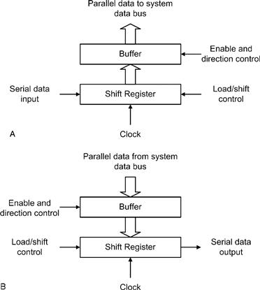
Figure 33.9 (A) Serial-to-parallel data conversion, and (B) parallel-to-serial data conversion
33.8.3 An Example Program
The following example program (see Table 33.3) is written in assembly code. The program transfers 8-bit data from an input port (Port A), complements (i.e., inverts) the data (by changing 0’s to 1’s and 1’s to 0’s in every bit position) and then outputs the result to an output port (Port B). The program repeats indefinitely.
Table 33.3 A simple example program
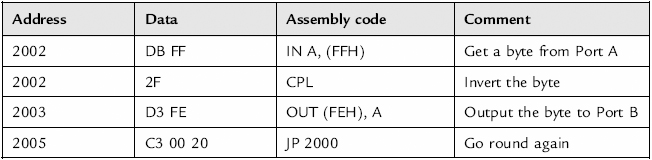
Just three microprocessor instructions are required to carry out this task together with a fourth (jump) instruction that causes the three instructions to be repeated over and over again. A program of this sort is most easily written in assembly code which consists of a series of easy to remember mnemonics. The flowchart for the program is shown in Figure 33.10(A).

Figure 33.10 (A) Flowchart for the example program, and (B) the eight bytes of program code stored in memory
The program occupies a total of eight bytes of memory, starting at a hexadecimal address of 2000 as shown in Figure 33.10(B). You should also note that the two ports, A and B, each have unique addresses; Port A is at hexadecimal address FF while Port B is at hexadecimal address FE.
33.8.4 Interrupts
A program that simply executes a loop indefinitely has a rather limited practical application. In most microprocessor systems we want to be able to interrupt the normal sequence of program flow in order to alert the microprocessor to the need to do something. We can do this with a signal known as an interrupt. There are two types of interrupt; maskable and nonmaskable.
When a nonmaskable interrupt input is asserted, the processor must suspend execution of the current instruction and respond immediately to the interrupt. In the case of a maskable interrupt, the processor’s response will depend upon whether interrupts are currently enabled or disabled (when enabled, the CPU will suspend its current task and carry out the requisite interrupt service routine).
The response to interrupts can be enabled or disabled by means of appropriate program instructions. In practice, interrupt signals may be generated from a number of sources and since each will require its own customized response a mechanism must be provided for identifying the source of the interrupt and calling the appropriate interrupt service routine. In order to assist in this task, the microprocessor may use a dedicated programmable interrupt controller chip.
33.9 A Microcontroller System
Figure 33.11 shows the arrangement of a typical microcontroller system. The sensed quantities (temperature, position, etc.) are converted to corresponding electrical signals by means of a number of sensors. The outputs from the sensors (in either digital or analog form) are passed as input signals to the microcontroller. The microcontroller also accepts inputs from the user. These user set options typically include target values for variables (such as desired room temperature), limit values (such as maximum shaft speed), or time constraints (such as “on” time and “off” time, delay time, etc).
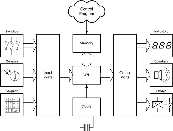
Figure 33.11 A microcontroller system with typical inputs and outputs
The operation of the microcontroller is controlled by a sequence of software instructions known as a control program. The control program operates continuously, examining inputs from sensors, user settings, and time data before making changes to the output signals sent to one or more controlled devices.
The controlled quantities are produced by the controlled devices in response to output signals from the microcontroller. The controlled device generally converts energy from one form into energy in another form. For example, the controlled device might be an electrical heater that converts electrical energy from the AC mains supply into heat energy thus producing a given temperature (the controlled quantity).
In most real-world systems there is a requirement for the system to be automatic or self-regulating. Once set, such systems will continue to operate without continuous operator intervention. The output of a self-regulating system is fed back to its input in order to produce what is known as a closed loop system. A good example of a closed-loop system is a heating control system that is designed to maintain a constant room temperature and humidity within a building regardless of changes in the outside conditions.
In simple terms, a microcontroller must produce a specific state on each of the lines connected to its output ports in response to a particular combination of states present on each of the lines connected to its input ports (see Figure 33.11). Microcontrollers must also have a central processing unit (CPU) capable of performing simple arithmetic, logical and timing operations.
The input port signals can be derived from a number of sources including:
• switches (including momentary action pushbuttons);
The output port signals can be connected to a number of devices including:
• LED indicators (both individual and multiple bar types);
• LED seven segment displays (via a suitable interface);
• motors and actuators (both linear and rotary types) via a suitable buffer/driver or a dedicated interface);
• relays (both conventional electromagnetic types and optically couple solid-state types); and
• transistor drivers and other solid-state switching devices.
33.9.1 Input Devices
Input devices supply information to the computer system from the outside world. In an ordinary personal computer, the most obvious input device is the keyboard. Other input devices available on a PC are the mouse (pointing device), scanner and modem. Microcontrollers use much simpler input devices. These need be nothing more than individual switches or contacts that make and break but many other types of device are also used including many types of sensor that provide logic level outputs (such as float switches, proximity detectors, light sensors, etc).
It is important to note that, in order to be connected directly to the input port of a microcontroller, an input device must provide a logic compatible signal. This is because microcontroller inputs can only accept digital input signals with the same voltage levels as the logic power source. The 0V ground level (often referred to as VSS in the case of a CMOS microcontroller) and the positive supply (VDD in the case of a CMOS microcontroller) is invariably 5V ± 5%. A level of approximately 0V indicates a logic 0 signal and a voltage approximately equal to the positive power supply indicates a logic 1 signal.
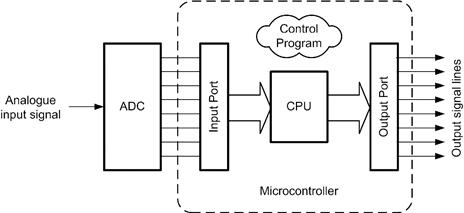
Figure 33.12 An analog input signal can be connected to a microcontroller input port via an analog-to-digital converter (ADC)
Other input devices may sense analog quantities (such as velocity) but use a digital code to represent their value as an input to the microcontroller system. Some microcontrollers provide an internal analog-to-digital converter (ADC) in order to greatly simplify the connection of analog sensors as input devices but where this facility isn’t available it will be necessary to use an external ADC which usually takes the form of a single integrated circuit. The resolution of the ADC will depend upon the number of bits used and 8, 10, and 12-bit devices are common in control applications.

Figure 33.13 An analog output signal can be produced by connecting a digital-to-analog converter (DAC) to a microcontroller output power
33.9.2 Output Devices
Output devices are used to communicate information or actions from a computer system to the outside world. In a personal computer system, the most common output device is the CRT (cathode ray tube) display. Other output devices include printers and modems. As with input devices, microcontroller systems often use much simpler output devices. These may be nothing more than LEDs, piezoelectric sounders, relays and motors. In order to be connected directly to the output port of a microcontroller, an output device must, once again, be able to accept a logic compatible signal.
Where analog quantities (rather than simple digital on/off operation) are required at the output a digital-to-analog converter (DAC) will be needed. All of the functions associated with a DAC can be provided by a single integrated circuit. As with an ADC, the output resolution of a DAC depends on the number of bits and 8, 10, and 12-bits are common in control applications.
33.9.3 Interface Circuits
Finally, where input and output signals are not logic compatible (i.e., when they are outside the range of signals that can be connected directly to the microcontroller) some additional interface circuitry may be required in order to shift the voltage levels or to provide additional current drive. Additional circuitry may also be required when a load (such as a relay or motor) requires more current than is available from a standard logic device or output port. For example, a common range of interface circuits (solid-state relays) is available that will allow a microcontroller to be easily interfaced to an AC mains-connected load. It then becomes possible for a small microcontroller (operating from only a 5V DC supply) to control a central heating system operating from 240V AC mains.