
Chapter 26
Useful Circuits
26.1 Introduction
Portable and single-supply electronic equipment is becoming more popular each day. The demand for single-supply op-amp circuits increases with the demand for portable electronic equipment because most portable systems have one battery. Split- or dual-supply op-amp circuit design is straightforward because op-amp inputs and outputs are referenced to the normally grounded center tap of the supplies. In the majority of split-supply applications, signal sources driving the op-amp inputs are referenced to ground, thus with one input of the op-amp referenced to ground, as shown in Figure 26.1, there is no need to consider input common-mode voltage problems.
 (26.1)

Figure 26.1 Split-supply op-amp circuit
When the signal source is not referenced to ground (see Figure 26.2 and Equation 26.19), the voltage difference between ground and the reference voltage shows up amplified in the output voltage. Sometimes this situation is OK, but other times the difference voltage must be stripped out of the output voltage.
 (26.2)
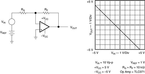
Figure 26.2 Split-supply op-amp circuit with reference voltage input
An input bias voltage is used to eliminate the difference voltage when it must not appear in the output voltage (see Figure 26.3 and Equation 26.3). The voltage, VREF, is in both input circuits, hence it is named a common-mode voltage. Voltage-feedback op-amps, like those used in this document, reject common-mode voltages because their input circuit is constructed with a differential amplifier (chosen because it has natural common-mode voltage rejection capabilities).
 (26.3)

Figure 26.3 Split-supply op-amp circuit with common-mode voltage
When signal sources are referenced to ground, single-supply op-amp circuits always have a large input common-mode voltage. Figure 26.4 shows a single-supply op-amp circuit that has its input voltage referenced to ground. The input voltage is not referenced to the midpoint of the supplies like it would be in a split-supply application, rather it is referenced to the lower power supply rail. This circuit malfunctions when the input voltage is positive because the output voltage would have to go negative—hard to do with a positive supply. It operates marginally with small negative input voltages because most op-amps do not function well when the inputs are connected to the supply rails.

Figure 26.4 Single-supply op-amp circuit
The constant requirement to account for inputs connected to ground or other reference voltages makes it difficult to design single-supply op-amp circuits. This chapter presents a collection of single-supply op-amp circuits, including their description and transfer equation. Those without a good working knowledge of op-amp equations should reference the Understanding Basic Analog … series of application notes available from Texas Instruments. Application note SLAA068, Understanding Basic Analog—Ideal Op-Amps develops the ideal op-amp equations. Circuit equations in this chapter are written with the ideal op-amp assumptions as specified in that document. The assumptions appear in Table 26.1 for easy reference.
Table 26.1 Ideal op-amp assumptions
| Parameter name | Parameter symbol | Value |
| Input current | IIN | 0 |
| Input offset voltage | VOS | 0 |
| Input impedance | ZIN | ∞ |
| Output impedance | ZOUT | 0 |
| Op-amp gain | a | ∞ |
Detailed information about designing single-supply op-amp circuits appears in application note SLOA030, Single-Supply Op-Amp Design Techniques. Unless otherwise specified, all op-amp circuits shown here are single-supply circuits. The single supply may be wired with the negative or positive lead connected to ground, but as long as the supply polarity is correct, the wiring does not affect circuit operation.
26.2 Boundary Conditions
All op-amps are constrained to output voltage swings less than or equal to their power supply. Use of a single supply limits the output voltage to the range of the supply voltage. For example, when the supply voltage VCC equals +10V, the output voltage is limited to the range 0 ≤ VOUT ≤ 10. This limitation precludes negative output voltages when the circuit has a positive supply voltage, but it does not preclude negative input voltages. As long as the voltage on the op-amp input leads does not become negative, the circuit can handle negative voltages applied to the input resistors.
Beware of working with negative (positive) input voltages when the op-amp is powered from a positive (negative) supply because op-amp inputs are highly susceptible to reverse-voltage breakdown. Also, ensure that no start-up condition reverse biases the op-amp inputs when the input and supply voltage are opposite polarity. It may be advisable to protect the op-amp inputs with a diode (Schottky or germanium) connected anode to ground and cathode to the op-amp input.
26.3 Amplifiers
Many types of amplifiers can be created using op-amps. This section consists of a selection of some basic, single-supply op-amp circuits that are available to the designer during the concept stage of a design. The circuit configuration and correct single-supply DC biasing techniques are presented for the following cases: inverting, noninverting, differential, T-network, buffer and AC-coupled amplifiers.
26.3.1 Inverting Op-Amp with Noninverting Positive Reference
The ideal transfer equation is given in Equation 26.4
 (26.4)
The transfer equation for this circuit (Figure 26.5) takes the form of Y = –mX + b. The transfer function slope is negative, and the DC intercept is positive. RF and RG are contained in both halves of the equation, thus it is hard to obtain the desired slope and DC intercept without modifying VREF. This is the minimum component count configuration for this transfer function. When the reference voltage is 0, the input voltage is constrained to negative voltages because positive input voltages would cause the output voltage to saturate at ground.

Figure 26.5 Inverting op-amp with noninverting positive reference
26.3.2 Inverting Op-Amp with Inverting Negative Reference
The transfer equation takes the form of Y = –mX + b and is given in Equation 26.5
 (26.5)
The transfer function slope is negative, and the DC intercept is positive (Figure 26.6). RG1 and RG2 are contained in the equation, thus it is easy to obtain the desired slope and DC intercept by adjusting the value of both resistors. Because of the virtual ground at the inverting input, RG2 is the terminating impedance for VREF. When the reference voltage is 0, the input voltage is constrained to negative voltages because positive input voltages would cause the output voltage to saturate at ground.

Figure 26.6 Inverting op-amp with inverting negative reference
26.3.3 Inverting Op-Amp with Noninverting Negative Reference
The transfer equation takes the form of Y = −mX − b and is given in Equation 26.6
 (26.6)
The transfer function slope is negative, and the DC intercept is negative. RF and RG are contained in both halves of the equation, thus it is hard to obtain the desired slope and DC intercept without modifying VREF. This is the minimum component count configuration for this transfer function. The slope and DC intercept terms in Equation 26.6 are both negative, hence, unless the correct input voltage range is selected, the output voltage will saturate at ground. The negative input voltage must be limited to less than −400 mV because op-amp inputs either break down or have protection circuits that forward bias when large negative voltages are applied to the inputs.

Figure 26.7 Inverting op-amp with noninverting negative reference
26.3.4 Inverting Op-Amp with Inverting Positive Reference
The transfer equation takes the form of Y = −mX − b and is given in Equation 26.7
 (26.7)
The transfer function slope is negative, and the DC intercept is negative. RG1 and RG2 are contained in the equation, thus it is easy to obtain the desired slope and DC intercept by adjusting the value of both resistors. Because of the virtual ground at the inverting input, RG2 is the terminating impedance for VREF. The slope and DC intercept terms in Equation 26.7 are both negative, hence, unless the correct input voltage range is selected, the output voltage will saturate.
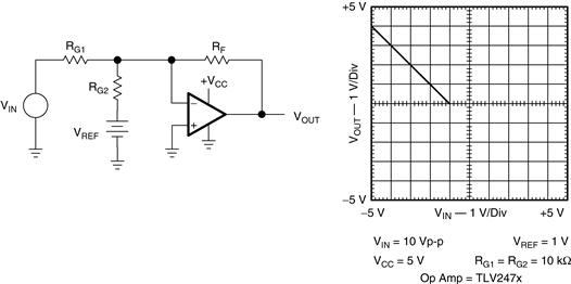
Figure 26.8 Inverting op-amp with inverting positive reference
26.3.5 Noninverting Op-Amp with Inverting Positive Reference
The transfer equation takes the form of Y = mX – b and is given in Equation 26.8
 (26.8)
The transfer function slope is positive, and the DC intercept is negative. This is the minimum component count configuration for this transfer function. The reference termination resistor is connected to a virtual ground, so RG is the load across VREF. RF and RG are contained in both halves of the equation, thus it is hard to obtain the desired slope and DC intercept without modifying VREF or placing an attenuator in series with VIN.

Figure 26.9 Noninverting op-amp with inverting positive reference
26.3.6 Noninverting Op-Amp with Noninverting Negative Reference
The transfer equation takes the form of Y = mX – b and is given in Equation 26.9.
 (26.9)
The transfer function slope is positive, and the DC intercept is negative. The reference is terminated in R1 and R2. R1 and R2 can be selected independent of RF and RG to obtain the desired slope and DC intercept. The price for the extra degree of freedom is two resistors.

Figure 26.10 Noninverting op-amp with noninverting negative reference
26.3.7 Noninverting Op-Amp with Inverting Negative Reference
The transfer equation takes the form of Y = mX + b and is given in Equation 26.10
 (26.10)
The transfer function slope is positive, and the DC intercept is positive. This is the minimum component count configuration for this transfer function. The reference termination resistor is connected to a virtual ground, so RG is the load across VREF. RF and RG are contained in both halves of the equation. Thus, it is hard to obtain the desired slope and DC intercept without modifying VREF or placing an attenuator in series with VIN.

Figure 26.11 Noninverting op-amp with inverting positive reference
26.3.8 Noninverting Op-Amp with Noninverting Positive Reference
The transfer equation takes the form of Y = mX + b and is given in Equation 26.11
 (26.11)
The transfer function slope is positive, and the DC intercept is positive. The reference is terminated in R1 and R2. R1 and R2 can be selected independent of RF and RG to obtain the desired slope and DC intercept. The price for the extra degree of freedom is two resistors.

Figure 26.12 Noninverting op-amp with noninverting positive reference
26.3.9 Differential Amplifier
When RF is set equal to R2 and RG is set equal to R1, Equation 26.12 reduces to Equation 26.13
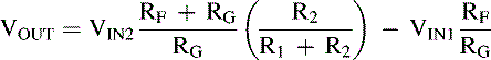 (26.12)
 (26.13)
These resistors must be matched very closely to obtain good differential performance. The mismatch error in these resistors reduces the common-mode performance, and the mismatch shows up in the output as an amplified common-mode voltage.
Consider Equation 26.13 Note that only the difference signal is amplified, thus this configuration is called a differential amplifier. The differential amplifier is a popular circuit in precision applications where it is used to amplify sensor outputs while rejecting common-mode noise.
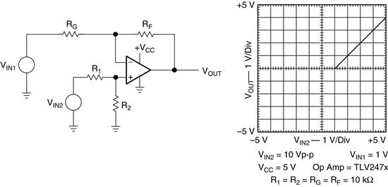
Figure 26.13 Differential amplifier
The inverting input impedance is RG because of the virtual ground at the inverting op-amp input. The noninverting input impedance is RF + RG because the noninverting op-amp input impedance approaches infinity. The two input impedances are different, and this leads to two problems with this circuit.
First, mismatched input impedances preclude any attempts to cancel input bias currents through resistor matching. Often R2 is set equal to RF || RG so that the bias currents develop equal common-mode voltages which the op-amp rejects. This is not possible when R2 = RF and R1 = RG unless the source impedances are matched. Second, high output impedance sensors are often used, and when high output sensors work into mismatched input impedances, errors occur.
26.3.10 Differential Amplifier with Bias Correction
When RF is set equal to R2 and RG is set equal to R1, Equation 26.14 reduces to Equation 26.15
 (26.14)
 (26.15)
When an offset voltage must be eliminated from or added to the input signal, this differential amplifier circuit is employed. The reference voltage can be positive or negative depending upon the polarity offset required, but care must be taken to protect the op-amp inputs and not exceed the output range.

Figure 26.14 Differential amplifier with bias correction
26.3.11 High Input Impedance Differential Amplifier
When RF is set equal to R1 and RG is set equal to R2, Equation 26.16 reduces to Equation 26.17
 (26.16)
 (26.17)
Each input signal is connected to an op-amp noninverting input that is very high impedance. The input impedance of the circuit is very high, and it is matched, so this circuit is often used to interface to high-impedance sensors. Each op-amp has a signal propagation time, and VIN1 experiences two propagation delays versus VIN2’s one propagation delay. At high frequencies, the propagation delay becomes a significant portion of the signal period, and this configuration is not usable at that frequency.
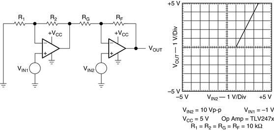
Figure 26.15 High input impedance differential amplifier
RF and R2, and RG and R1 should be matched to achieve good common-mode rejection capability. Bias current cancellation resistors equal to RF || RG should be connected in series with the input sources for precision applications.
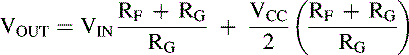
26.3.12 High Common-Mode Range Differential Amplifier
When all resistors are equal, Equation 26.18 reduces to Equation 26.19
 (26.18)
![]() (26.19)
(26.19)
R1 and RG2 are equal-value resistors terminated into a virtual ground; hence, the input sources are equally terminated. This configuration has high common-mode capability because R1 and RG2 limit the current that can flow into or out of the op-amp. Thus, the input voltage can rise to any value that does not exceed the op-amp’s drive capability. The voltage references, VREF1 and VREF2, are added for bias purposes. Without bias, the output voltage of the op-amps would saturate at ground, and the bias voltages keep the output voltage of the op-amp positive.
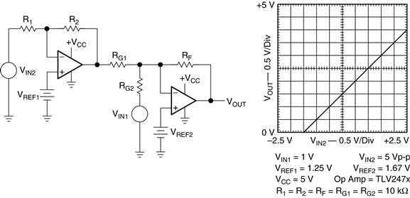
Figure 26.16 High common-mode range differential amplifier
26.3.13 High-Precision Differential Amplifier
When R7 = R6, R5 = R2, R1 = R4, and VREF1 = VREF2, Equation 26.20 reduces to Equation 26.21
 (26.20)
 (26.21)

Figure 26.17 High-precision differential amplifier
In this circuit configuration, both sources work into the input impedance of a noninverting op-amp. This impedance is very high, and if the op-amps are identical, both impedances are very nearly equal. The propagation delay is still equal to two op-amp propagation delays, but the propagation delay is very nearly equal, so any distortion resulting from unequal propagation delays is minimized.
The equal resistors should be matched with more precision than is expected from the circuit. Resistor matching eliminates distortion due to unequal gains, and it reduces the common-mode voltage feed through. Resistors equal to (R1 || R3)/2 may be placed in series with the sources to reduce errors resulting from bias currents. This differential amplifier has the unique feature that the gain can be changed with only one resistor, and if the gain setting resistor is R3, no resistor matching is required to change gain.
26.3.14 Simplified High-Precision Differential Amplifier
When RF is set equal to R2, RG is set equal to R1, and VREF1 = VREF2, Equation 26.22 reduces to Equation 26.23
 (26.22)
 (26.23)
Both input sources are loaded equally with very high impedances in the simplified high precision differential amplifier. This configuration eliminates three resistors, two of which are matched, but it sacrifices flexibility in gain setting capability because the gain must be set with a matched pair of resistors.

Figure 26.18 Simplified high-precision differential amplifier
26.3.15 Variable Gain Differential Amplifier
When R1 is set equal to R3 and R2 is set equal to R4, Equation 26.24 reduces to Equation 26.25
 (26.24)
 (26.25)
When a function is enclosed in a feedback loop, the function acts inverted on the closed loop transfer function. Thus, the gain stage RF/RG ends up being an attenuator. The circuit shown in Figure 26.19 can be used with any of the differential amplifiers to change gain without affecting matched resistors. R1, R3 and R2, R4 must be matched to reduce the common-mode voltage.

Figure 26.19 Variable gain differential amplifier
26.3.16 T Network in the Feedback Loop
Sometimes it is desirable to have a low-resistance path to ground in the feedback loop. Standard inverting op-amps cannot do this when the driving circuit sets the input resistor value and the gain specification sets the feedback resistor value. Inserting a T network in the feedback loop yields a degree of freedom that enables both specifications to be met with a low DC resistance path to ground in the feedback loop.
 (26.26)
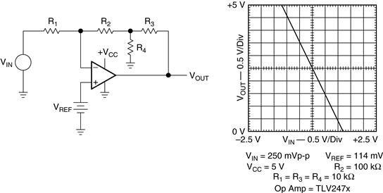
Figure 26.20 T network in the feedback loop
26.3.17 Buffer
The buffer input signal polarity must be unipolar because the output voltage swing is unipolar. When this limitation precludes the buffer, a differential amplifier with the negative input correctly biased is used, or a reference voltage is added to the buffer to offset the output voltage. RF must be included when the op-amp inputs are not rated for the full supply voltage. In that case, RF limits the current into the op-amp inputs, thus preventing latch up. Most new op-amp inputs can withstand the full supply voltage, so they often leave RF out as cost savings. The main attraction of the buffer is that it has very high input impedance and very low output impedance. The impedance transformation capability is why buffers are often added to the input of other circuits.
![]() (26.27)
(26.27)

Figure 26.21 Buffer
26.3.18 Inverting AC Amplifier
VCC and resistors R set a DC level of VCC/2 at the inverting input. RG is connected to ground through a capacitor, thus the circuit functions as a buffer for DC. This causes the DC output voltage to be VCC/2, so the quiescent output voltage is the middle of the supply voltage, and it is ready to swing to either rail as the input signal commands.
The AC gain is given in Equation 26.28 RG and C form a coupling network for the AC signal. Good coupling networks should be constant low impedance at the signal frequencies, so Equation 26.29 should be satisfied to get good low-frequency performance. The lowest frequency component of the input signal, fMIN, is determined by completing a Fourier series on the input signal. Then, setting fMIN = 100f in Equation 26.29 ensures that the 3-dB breakpoint introduced by RG and C is two decades lower than fMAX.
 (26.28)
 (26.29)

Figure 26.22 Inverting AC amplifier
26.3.19 Noninverting AC Amplifier
VCC and the resistors (R) set a DC level of VCC/2 at the inverting input. RG is connected to ground through a capacitor, thus the circuit functions as a buffer for DC. This causes the DC output voltage to be VCC/2, so the quiescent output voltage is the middle of the supply voltage, and it is ready to swing to either rail as the input signal commands.
The AC gain is given in Equation 26.30 RG and C create a coupling network for the AC signal. Good coupling networks should be a constant low impedance at the signal frequencies, so Equation 26.31 should be satisfied to get good low frequency performance. The lowest frequency component of the input signal, fMIN, is determined by completing a Fourier series on the input signal. Then, setting fMIN = 100f in Equation 26.31 ensures that the 3-dB breakpoint introduced by RG and C is two decades lower than fMAX. The breakpoint for RG and C1 is set in a similar manner.
 (26.30)
 (26.31)

Figure 26.23 Noninverting AC amplifier
26.4 Computing Circuits
Four versions of the inverting op-amp and four versions of the noninverting op-amp were given in the previous section. During the concept stage of the design, one of these eight op-amp circuits is selected. Specifications for the input and output voltage are the selection criteria that determines which circuit configuration is used.
There are four versions of most of the circuits given in this and following sections, but just the simplest version of any circuit is included in this chapter because of space limitations. Each circuit configuration can be modified as required to fit specific applications. Look back to the first section to determine what bias is required to fit the application, and adapt that bias to the new circuit.
26.4.1 Inverting Summer
The three input voltages are inverted and added as Equation 26.32 shows. RB should be made equal in value to the parallel combination of RF, RG1, RG2, and RG3 to convert the input bias current to a common-mode voltage so the op-amp can reject it. VREF sets the output voltage somewhere between the supply limits, and this allows negative addition (subtraction) to take place.
 (26.32)
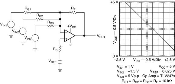
Figure 26.24 Inverting summer
26.4.2 Noninverting Summer
This circuit adds the input voltages and multiplies them by the stage gain. RG1, RG2, and RG3 in parallel should be equal to RF in parallel with RG to cancel the input bias current using the common-mode input voltage rejection technique. VREF is added to the circuit to enable the addition of negative values.
 (26.33)
Figure 26.25 Noninverting summer
26.4.3 Noninverting Summer with Buffers
VREF1 and VREF2 are added to enable the buffers to handle positive input voltages. Their output contribution to the last stage is cancelled out by VREF3. This configuration uses fewer resistors at the expense of two op-amps. RG1, RG2, and RF in parallel should be made equal to RB to cancel the input bias current.
 (26.34)

Figure 26.26 Noninverting summer with buffers
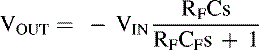
26.4.4 Inverting Integrator
The Laplace operator, s = jω, is used in Equation 26.35, and the mathematical operation 1/s constitutes an integration. Differentiation circuits are shown later, and the mathematical operation, s, constitutes a differentiation. The integration time constant is RC, thus the magnitude crosses 0 dB on a log plot when RC = 1. Also the phase is −45° when RC = 1.
![]() (26.35)
(26.35)
This integrator is not very practical because there is no method of discharging the capacitor; hence, any leakage current will eventually charge the capacitor until the circuit becomes saturated. The positive input of the integrator is biased at VCC/2 to center the output voltage at VCC/2; thus allowing for positive and negative voltage swings. The bias resistors are selected as 2R so that the parallel combination equals R. This offsets the input current drawn through R.
26.4.5 Inverting Integrator with Input Current Compensation
Functionally, this circuit is the same as that shown in Figure 26.27, but a current compensation network has been added to offset the input current. VCC, R1, and R2 bias the positive input at VCC/2 to center the output voltage at VCC/2; thus allowing for positive and negative voltage swings.
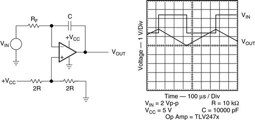
Figure 26.27 Inverting integrator
R1 and R2 are selected as relatively small values because the current flowing through RA also flows through the parallel combination of R1 and R2. RA forward biases the diode with a constant current, thus the diode acts like a small voltage regulator. The diode voltage drop is temperature sensitive, and this factor works in our favor because the input transistors are temperature sensitive. The two temperature sensitivities cancel out if the diode current is selected correctly. RB is a large-value resistor that acts like a current source, so it is selected such that it supplies the input bias current. Selecting RB correctly ensures that no input current flows through the integration resistor, R.
This integrator is not very practical because there is no method of discharging the capacitor. Hence, any input current will eventually charge the capacitor until the circuit becomes saturated. The bias circuit drastically reduces the input current flowing through R, thus it extends the integration time. A reset circuit is needed to make the integrator more practical.
This bias compensation scheme is set up for an op-amp that has NPN input transistors. The diode must be reversed and connected to ground for op-amps with PNP input circuits.
![]() (26.36)
(26.36)

Figure 26.28 Inverting integrator with input current compensation
26.4.6 Inverting Integrator with Drift Compensation
Functionally, this circuit is the same as that shown in Figure 26.27, but it uses an RC circuit in the positive lead to obtain drift compensation. The voltage divider is made from a series string of resistors (RA), and VCC biases the input in the center of the power supply.
Positive input current flows through R and C in parallel, so the positive input current drops the same voltage across the parallel RC combination as the negative input current drops across its series RC combination. The common-mode rejection capability of the op-amp rejects the voltages caused by the input currents. Much longer integration times can be achieved with this circuit, but when the input signal does not center around VCC/2, the compensation is poor.
![]() (26.37)
(26.37)

Figure 26.29 Inverting integrator with drift compensation
26.4.7 Inverting Integrator with Mechanical Reset
Functionally, this circuit is the same as that shown in Figure 26.27, but a method has been provided to discharge (reset) the capacitor. S1 is a mechanical switch or relay and when the contacts close, they short the integrating capacitor forcing it to discharge. Some capacitors are sensitive to fast discharge cycles, so RS is put in the discharge path to limit the initial discharge current. When RS is absent from the circuit, the impulse of current that occurs at the first instant of discharge causes considerable noise, so the selection of RS is also based on noise considerations. For all practical purposes, the time constant formed by RS and C determines the discharge rate.

Figure 26.30 Inverting integrator with mechanical reset
One advantage of mechanical discharge methods is that they are isolated from the remainder of the circuit. Their size, weight, time delay, and uncertain actuating time offset this advantage. When the disadvantages of mechanical reset outweigh the advantages, circuit designers go to electronic reset circuits.
![]() (26.38)
(26.38)
26.4.8 Inverting Integrator with Electronic Reset
Functionally, this circuit is the same as that shown in Figure 26.27, but an electronic method has been provided to discharge (reset) the capacitor. Q1 is controlled by a gate drive signal that changes its state from on to off. When Q1 is on, the gate-source resistance is low, less than 100Ω. And when Q1 is off, the gate-source resistance is high—about several hundred MΩ.
The source of the FET is at the inverting lead that is at ground, so the Q1 gate-source bias is not affected by the input signal. Sometimes, the output signal can get large enough to cause leakage currents in Q1, so the designer must take care to bias Q1 correctly. Consult a transistor book for more detailed information on transistor reset circuits. A major problem with electronic reset is the charge injected through the transistor’s stray capacitance. This charge can be large enough to cause integration errors.
![]() (26.39)
(26.39)

Figure 26.31 Inverting integrator with electronic reset
26.4.9 Inverting Integrator with Resistive Reset
This circuit differs from that shown in Figure 26.27 because it yields a breakpoint rather than a pure integration. On a log plot, the integrator slope is −6 dB per octave at the 0 frequency intercept, and the 0 dB intercept occurs when f = 1/2πRC. A breakpoint plots flat on a log plot until the breakpoint where it breaks down at −6 dB per octave. It is −3 dB when f = 1/2πRC.
RF is in parallel with the integrating capacitor, C, so it is continually discharging C. The low frequency attenuation that is the best attribute of the pure integrator is sacrificed for the reset circuit complexity:
 (26.40)
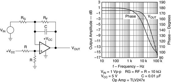
Figure 26.32 Inverting integrator with resistive reset
26.4.10 Noninverting Integrator with Inverting Buffer
This circuit is an inverting integrator preceded by an inverting buffer. Eliminating the signal inversion costs an op-amp and four resistors, but this is the easiest way to get true noninverting integrator performance.
 (26.41)
26.4.11 Noninverting Integrator Approximation
This circuit has fewer parts than the Noninverting Integrator with Inverting Buffer (Figure 26.33), but it is not a true integrator because there is a zero in the transfer equation. The log plot starts rolling off at a −6 dB per octave rate at low frequencies, but when f = 1/2πRC, the zero cuts in. The zero causes the log plot to flatten out because the slope decreases to 0 db per decade.

Figure 26.33 Noninverting integrator with inverting buffer
This circuit functions as an integrator at very low frequencies, but at frequencies higher than f = 1/2πRC, it functions as a buffer.
![]() (26.42)
(26.42)

Figure 26.34 Noninverting integrator approximation
26.4.12 Inverting Differentiator
The log plot of the differentiator is a positive slope of 6-dB per octave passing through 0 dB at f = 1/2πRC. At extremely high frequencies, the capacitive reactance goes to very low values, thus the circuit gain approaches the op-amp open-loop gain. This performance emphasizes any system noise or noise generated by the op-amp. The poor noise performance of this circuit limits its application to a very few specialized situations.
This configuration has a pole in the feedback loop. If the op-amp has more than one pole, and most op-amps have several poles, this configuration can become oscillatory. The VCC and RA circuit bias the output in the center of the power supplies. RA/2 should be selected equal to RG||RF so that input currents are canceled out.
![]() (26.43)
(26.43)

Figure 26.35 Inverting differentiator
26.4.13 Inverting Differentiator with Noise Filter
This circuit has a pure differentiator that rises at a 6-dB per octave slope from zero frequency. At f = 1/2πRFCF, the pole kicks in and the slope is reduced to zero. The pole has two effects. First, it stabilizes the circuit by canceling zero’s phase shift. Second, it limits the circuit gain to 1 at high frequencies, so it acts like a noise filter.
R/2 should equal RF for good input current cancellation, and VCC coupled with R centers the output voltage.
 (26.44)

Figure 26.36 Inverting differentiator with noise filter
26.5 Oscillators
This section describes some general op-amp sinewave oscillator circuits that fall under three main categories: Wien bridge, phase shift, and quadrature. A brief description and of each type is provided, along with one or two variations. Op-amp sinewave oscillators are used to create references in applications such as audio and function/waveform generators.
26.5.1 Basic Wien Bridge Oscillator
When ω = 2πf = 1/RC, the feedback is in phase (this is positive feedback), and the gain is 1/3, so oscillation requires an amplifier with a gain of 3. When RF = 2RG the amplifier gain is 3 and oscillation occurs at f = 1/2πRC. Normally, the gain is larger than 3 to ensure oscillation under worst case conditions.
VREF sets the output DC voltage in the center of the span.
The output sine wave is highly distorted because limiting by saturation and cut-off is controlling the output voltage excursion. The distortion decreases when the gain is decreased, but the circuit may not oscillate under worst-case low gain conditions.
 (26.45)

Figure 26.37 Basic Wien bridge oscillator
26.5.2 Wien Bridge Oscillator with Nonlinear Feedback
When the circuit gain is 3, RL = RF/2.
Substituting a lamp (RL) for the gain setting resistor reduces distortion because the nonlinear lamp resistance adjusts the gain to keep the output voltage smaller than the power supply voltage. The output voltage never approaches the power supply rail, so distortion doesn’t occur. RF and RL determine the lamp current (see Equations 26.46 and 26.47).
 (26.46)
 (26.47)

Figure 26.38 Wien bridge oscillator with nonlinear feedback
The lamp is selected by examining lamp resistance curves until a lamp with a resistance approximately equal to RF/2 at IOUT(RMS) is found. The output voltage swing should be less than 75% of the maximum guaranteed voltage swing, and 3 RL must be greater than the load resistance specified for the voltage swing specification. VREF should be VCC/5.
26.5.3 Wien Bridge Oscillator with AGC
The op-amp is configured as an AC amplifier to ease biasing problems. The gain equation for the op-amp is given below. RG1 or RG2, but not both resistors, is required depending on the selection of the Q1.
The diode, D1, half-wave rectifies the output voltage and applies it to the voltage divider formed by R1 and R2. The voltage divider biases Q1 in its linear region, and they eventually set the output voltage. C1 filters the rectified sine wave with a long time constant so that the output voltage stays constant. C2 must be selected large enough to act as a short at the oscillation frequency.
As the output voltage increases, the negative voltage across the gate of Q1 increases. The increased negative gate voltage causes Q1 to increase its drain-to-source resistance. This results in increased op-amp gain and an output voltage decrease. When the voltage divider and FET are selected properly, the output voltage swing is less than the guaranteed maximum swing, so distortion doesn’t occur.
 (26.48)
26.5.4 Quadrature Oscillator
Quadrature oscillators produce sine waves 90° out of phase, so they output sine/cosine, or quadrature waves.
When R1C1 = R2C2 = R3C3, the circuit oscillates at ω = 2πf = 1/RC. Both op-amps act as integrators causing two poles at 1/RC, thus the circuit oscillates when the loop gain crosses the 0-dB axis. The integrators ensure that gain is always sufficient for oscillation. There is a slight bit of distortion at the sine output, and it is very hard to eliminate this distortion.
26.5.5 Classical Phase Shift Oscillator
Theoretically, the three RC sections do not load each other, thus the loop gain has three identical poles multiplied by the op-amp gain.
The loop phase shift is −180° when the phase shift of each section is −60°, and this occurs when ω = 2πf = 1.732/RC because the tangent of 60° = 1.73. The magnitude of β at this point is (1/2)3, so the gain, A = RF/RG, must be greater or equal to 8 for the system gain to be equal to 1.
The assumption that the RC sections do not load each other is not entirely valid, thus the circuit does not oscillate at the specified frequency, and the gain required for oscillation is more than 8. This circuit configuration was very popular when an active component was large and expensive, but now that op-amps are inexpensive, small, and come quad packages, the classical phase shift oscillator is losing popularity
The classical phase shift oscillator has an undistorted sine wave available at the output of the third RC section. This is not a low-impedance output, and the signal amplitude is smallest here, but these sacrifices have to be made to get away from distortion. An undistorted output can be obtained from the op-amp if an AGC circuit similar to the one shown in Figure 26.39 is employed. The reference voltage is set according to the equation VREF = VCC/ 2(1 + RF/RG) to center the output voltage at VCC/2.
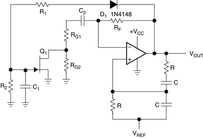
Figure 26.39 Wien bridge oscillator with AGC

Figure 26.40 Quadrature oscillator
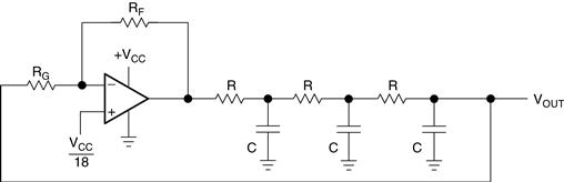
Figure 26.41 Classical phase shift oscillator
 (26.49)
26.5.6 Buffered Phase Shift Oscillator
A noninverting op-amp buffers each RC section in this oscillator. Equation 26.49, repeated below, truly represents the transfer function of this circuit if RG >> R.
 (26.50)
The loop phase shift is −180° when the phase shift of each section is −60°, and this occurs when ω = 2πf = 1.732/RC because the tangent 60° = 1.73. The magnitude of β at this point is (1/2)3, so the gain, A = RF/RG, must be greater or equal to 8 for the system gain to be equal to one.

Figure 26.42 Buffered phase shift oscillator
The buffered phase shift oscillator has an undistorted sine wave available at the output of the third RC section. This is not a low-impedance output, and the signal amplitude is smallest here, but these sacrifices have to be made to get away from distortion. An undistorted output can be obtained from the op-amp if an AGC circuit similar to the one shown in Figure 26.39 is employed.
There are three op-amps, so the gain can be distributed among the op-amps at the expense of a few resistors, and the distortion is reduced. Another method of reducing distortion is to limit the output voltage swing softly with external components. The limiting technique does not yield as good results as the AGC technique does, but it is less expensive. The reference voltage is set according to the equation VREF = VCC/ 2(1 + RF/RG) to center the output voltage at VCC/2.
26.5.7 Bubba Oscillator
The Bubba oscillator is another phase shift oscillator, but it takes advantage of the quad op-amp package to yield some unique advantages. Each RC section is buffered by an op-amp to prevent loading. When RG >> R there is no loading in the circuit, and the circuit yields theoretical performance.
Four RC sections require −45° phase shift per section to accumulate −180° phase shift. Each RC section contributes −45° phase shift when ω = 1/RC. The gain required for oscillation is G ≥ (1/0.707)4= 4. Taking outputs from alternate sections yields low-impedance quadrature outputs. When an output is taken from each op-amp, the circuit delivers four 45° phase-shifted sine waves.
The gain, A, must equal 4 for oscillation to occur. Very low distortion sine waves can be obtained from the junction of R and RG. When low-distortion sine waves are required at all outputs, the gain should be distributed among the op-amps. Gain distribution requires biasing of the other op-amps, but it has no effect on the oscillator frequency. This oscillator has the best dφ/df of the phase shift oscillators, so it has minimum frequency drift. The reference voltage is set according to the equation VREF = VCC/2(1 + RF/RG) to center the output voltage at VCC/2.
 (26.51)

Figure 26.43 Bubba oscillator
26.5.8 Triangle Oscillator
The triangle oscillator produces triangle waves and square waves. The op-amp functions as an integrator. When the output voltage of the comparator is low, the output of the op-amp charges C until the output voltage exceeds the hysteresis voltage set by R1 and RF and the reference voltage (VCC/2). At this point, the comparator output switches to a high state and the op-amp integrates the voltage in a negative direction. The triangle wave (op-amp output voltage swing) is given in Equation 26.52. The frequency of oscillation is given in Equation 26.53.
 (26.52)
 (26.53)
The op-amp reference voltage can be adjusted to equalize the triangle rise and fall times.

Figure 26.44 Triangle oscillator
26.6 Some Favorite Circuits
Every engineer has their favorite batch of circuits and I’m no exception. There are tons of circuit cookbooks out there that show how to implement no end of cool features. There are so many that you could spend all your time searching them and never getting anything done. I suggest you develop your own favorite basic circuits that you know well and intuitively understand. This is simply an extension of the “Lego” philosophy that was discussed earlier in this book. Here are a few of my favorites. These are in addition to all the circuits used as examples up to this point; one reason they make such good examples is that they are so useful.
26.6.1 Hybrid Darlington Pair
Cool application note, using two transistors to switch a signal level Vcc PNP switched by NPN (see Figure 26.45).

Figure 26.45 Vcc PNP switched by NPN
This is a handy circuit that switches a higher level voltage with a lower level one. Say, for example, you have a micro with a 5V output and you need to drive a 12V load. For a reason you can’t change, you have to switch the Vcc leg. In this circuit you turn on one transistor with a 5V signal, which in turn activates the other transistor switching the higher voltage to the load. This works because the transistors are current driven; when you shut off the current flow to the PNP transistor, it shuts off regardless of the voltage. Another plus is that this circuit has Darlington-like properties without one of the downsides. You won’t need a lot of current to the input to switch the output and, unlike a traditional Darlington pair, the voltage drop across the output is much smaller. You don’t have two series base junctions to contend with at the output.
26.6.2 DC Level Shifter
This is really the high-pass filter that we have already studied but with a slight twist. Instead of ground, we hook the resistor to a reference voltage. Since DC has a frequency of zero, only the AC component will pass and in the process a DC bias will be applied to the signal. Make sure you don’t size the cap and resistor so that the signal you want is attenuated.
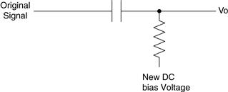
Figure 26.46 Change the DC bias on an AC signal
26.6.3 Virtual Ground
Using the voltage divider as a reference, the op-amp becomes a voltage source with the output matching the voltage at the divider. This can be very useful when you are trying to handle AC signals with only a single-ended supply circuit.

Figure 26.47 Create a “ground” at any level you want
26.6.4 Voltage Follower
This one is mighty useful when trying to measure a signal that is easily affected by load. Vi = Vo, but, best of all, Vi isn’t loaded at all, thanks to the buffering effect of the op-amp.

Figure 26.48 Voltage follower
This is another great circuit that works nicely amplifying AC signals with a single-ended supply. It also has the benefit of not amplifying any DC signal components, keeping things like DC offsets from making your signal rail. This happens because of the cap in the feedback circuit. Since the cap only passes AC current, DC signals see that point as disconnected. When the resistor to ground is disconnected, the op-amp acts like the voltage follower in the previous circuit.

Figure 26.49 AC only amplifier
26.6.5 Inverter Oscillator
I saw this in the back of a data book years ago; I think it was a Motorola logic data book. This was way back before the internet—you used to have to turn pages to find this stuff! The way it works is based on the fact that the Schmidt trigger inverter has hysteresis built into the input. This makes the output stick at a high or low level till the cap on the input charges to the threshold voltage that trips the inverter. Output flips and everything goes the other direction, repeating indefinitely. Adding some diodes to the charge and discharge path can affect the duty cycle of the output.

Figure 26.50 Schmidt trigger oscillator
26.6.6 Constant Current Source
Using negative feedback, the op-amp tries to maintain the voltage drop across R input. Even if the resistance of the load changes, the drop across the R input stays the same. According to Ohm’s Law, keeping R and V the same will keep current the same too. Remember, though, this current control has operational limits; it can only swing the output voltage so far to compensate for load variance. Once these limits are reached, the current regulation can no longer exist.

Figure 26.51 Voltage-controlled constant current source
References
1. Everyone learns from many sources. I have read many books that helped to gain that insight. Here is a list of those books, with a few comments to help you decide if you want to read them yourself.
2. Yellow Control Theory, Fundamentals of Automatic Control, by Robert C. Weyrick, McGraw Hill, ISBN 0-07-069493-1. Good read, helped me understand control theory.
3. “Pink Motor Book”— DC Motors Speed Controls Servo Systems: The Electro-Craft Engineering Handbook, by Reliance Motion Control, Inc. I like to call it the pink motor book due to an interesting choice of color for the cover, and I highly recommend it for anyone who is working with DC motors. It’s heavy on the equations, but a good source for understanding all the complexities of motors.
4. Grounding and Shielding Electronic Systems, by Dr. Tom Van Doren, University Missouri Rolla, Van Doren Company, Rt. 6, Box 319, Rolla, MO 65401, Ph 314-341-4097.
5. Intuitive IC Op-Amps, by Tom Frederickson. This clasic paperback book was originally published in 1984. The book describes how op-amps work and how they are used, from a practical, commonsense perspective. It is currently out of print. However, you may be able to find it in university libraries or by browsing the Internet. As of March 2005, the book was also available from Rector Press.
6. This book was written by the inventor of the most widely used op-amp in the world, the LM324. This book gave me the first hint that op-amps should be easy to use, not hard.