
Chapter 16
DSP and Digital Filters
16.1 Origins of Real-World Signals and Their Units of Measurement
Let’s first look at a few key concepts and definitions required to lay the groundwork for things to come.
Webster’s New Collegiate Dictionary defines a signal as “a detectable (or measurable) physical quantity or impulse (as voltage, current, or magnetic field strength) by which messages or information can be transmitted.” Key to this definition are the words: detectable, physical quantity, and information.
By their very nature, signals are analog, whether DC, AC, digital levels, or pulses. It is customary, however, to differentiate between analog and digital signals in the following manner: Analog (or real-world) variables in nature include all measurable physical quantities. In this book, analog signals are generally limited to electrical variables, their rates of change, and their associated energy or power levels. Sensors are used to convert other physical quantities such as temperature or pressure to electrical signals. The entire subject of signal conditioning deals with preparing real-world signals for processing, and includes such topics as sensors (temperature and pressure, for example), isolation amplifiers, and instrumentation amplifiers (Ref. 16.1).
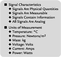
Figure 16.1 Signal characteristics
Some signals result in response to other signals. A good example is the returned signal from a radar or ultrasound imaging system, both of which result from a known transmitted signal.
On the other hand, there is another classification of signals, called digital, where the actual signal has been conditioned and formatted into a digit. These digital signals may or may not be related to real-world analog variables. Examples include the data transmitted over local area networks (LANs) or other high speed networks.
In the specific case of digital signal processing (DSP), the analog signal is converted into binary form by a device known as an analog-to-digital converter (ADC). The output of the ADC is a binary representation of the analog signal and is manipulated arithmetically by the digital signal processor. After processing, the information obtained from the signal may be converted back into analog form using a digital-to-analog converter (DAC).
Another key concept embodied in the definition of signal is that there is some kind of information contained in the signal. This leads us to the key reason for processing real-world analog signals: the extraction of information.
16.2 Reasons for Processing Real-World Signals
The primary reason for processing real-world signals is to extract information from them. This information normally exists in the form of signal amplitude (absolute or relative), frequency or spectral content, phase, or timing relationships with respect to other signals. Once the desired information is extracted from the signal, it may be used in a number of ways.
In some cases, it may be desirable to reformat the information contained in a signal. This would be the case in the transmission of a voice signal over a frequency-division multiple access (FDMA) telephone system. In this case, analog techniques are used to “stack” voice channels in the frequency spectrum for transmission via microwave relay, coaxial cable, or fiber. In the case of a digital transmission link, the analog voice information is first converted into digital using an ADC. The digital information representing the individual voice channels is multiplexed in time (time division multiple access, or TDMA) and transmitted over a serial digital transmission link (as in the T-carrier system).
Another requirement for signal processing is to compress the frequency content of the signal (without losing significant information), then format and transmit the information at lower data rates, thereby achieving a reduction in required channel bandwidth. High speed modems and adaptive pulse code modulation systems (ADPCM) make extensive use of data reduction algorithms, as do digital mobile radio systems, MPEG recording and playback, and high definition television (HDTV).
Industrial data acquisition and control systems make use of information extracted from sensors to develop appropriate feedback signals which in turn control the process itself. Note that these systems require both ADCs and DACs as well as sensors, signal conditioners, and the DSP (or microcontroller). Analog Devices offers a family of MicroConverters™ that includes precision analog conditioning circuitry, ADCs, DACs, microcontroller, and FLASH memory all on a single chip.
In some cases, the signal containing the information is buried in noise, and the primary objective is signal recovery. Techniques such as filtering, autocorrelation, and convolution are often used to accomplish this task in both the analog and digital domains.

Figure 16.2 Reasons for signal processing
16.3 Generation of Real-World Signals
In most of the previous examples (the ones requiring DSP techniques), both ADCs and DACs are required. In some cases, however, only DACs are required where real-world analog signals may be generated directly using DSP and DACs. Video raster scan display systems are a good example. The digitally generated signal drives a video or RAMDAC. Another example is artificially synthesized music and speech. In reality, however, the real-world analog signals generated using purely digital techniques do rely on information previously derived from the real-world equivalent analog signals. In display systems, the data from the display must convey the appropriate information to the operator. In synthesized audio systems, the statistical properties of the sounds being generated have been previously derived using extensive DSP analysis of the entire signal chain, including sound source, microphone, preamp, and ADC.
16.4 Methods and Technologies Available for Processing Real-World Signals
Signals may be processed using analog techniques (analog signal processing, or ASP), digital techniques (digital signal processing, or DSP), or a combination of analog and digital techniques (mixed-signal processing, or MSP). In some cases, the choice of techniques is clear; in others, there is no clear-cut choice, and second-order considerations may be used to make the final decision.
With respect to DSP, the factor that distinguishes it from traditional computer analysis of data is its speed and efficiency in performing sophisticated digital processing functions such as filtering, FFT analysis, and data compression in real time.
The term mixed-signal processing implies that both analog and digital processing is done as part of the system. The system may be implemented in the form of a printed circuit board, hybrid microcircuit, or a single integrated circuit chip. In the context of this broad definition, ADCs and DACs are considered to be mixed-signal processors, since both analog and digital functions are implemented in each. Recent advances in very large scale integration (VLSI) processing technology allow complex digital processing as well as analog processing to be performed on the same chip. The very nature of DSP itself implies that these functions can be performed in real time.
16.5 Analog Versus Digital Signal Processing
Today’s engineer faces a challenge in selecting the proper mix of analog and digital techniques to solve the signal processing task at hand. It is impossible to process real-world analog signals using purely digital techniques, since all sensors, including microphones, thermocouples, strain gages, piezoelectric crystals, and disk drive heads are analog sensors. Therefore, some sort of signal conditioning circuitry is required in order to prepare the sensor output for further signal processing, whether it be analog or digital. Signal conditioning circuits are, in reality, analog signal processors, performing such functions as multiplication (gain), isolation (instrumentation amplifiers and isolation amplifiers), detection in the presence of noise (high common-mode instrumentation amplifiers, line drivers, and line receivers), dynamic range compression (log amps, LOGDACs, and programmable gain amplifiers), and filtering (both passive and active).
Several methods of accomplishing signal processing are shown in Figure 16.3. The top portion of the figure shows the purely analog approach. The latter parts of the figure show the DSP approach. Note that once the decision has been made to use DSP techniques, the next decision must be where to place the ADC in the signal path.

Figure 16.3 Analog and digital signal processing options
In general, as the ADC is moved closer to the actual sensor, more of the analog signal conditioning burden is now placed on the ADC. The added ADC complexity may take the form of increased sampling rate, wider dynamic range, higher resolution, input noise rejection, input filtering, programmable gain amplifiers (PGAs), and on-chip voltage references, all of which add functionality and simplify the system. With today’s high resolution/high sampling rate data converter technology, significant progress has been made in integrating more and more of the conditioning circuitry within the ADC/DAC itself. In the measurement area, for instance, 24-bit ADCs are available with built-in programmable gain amplifiers (PGAs) that allow full-scale bridge signals of 10 mV to be digitized directly with no further conditioning (e.g., AD773x series). At voice-band and audio frequencies, complete coder/decoders (codecs or analog front ends) are available with sufficient on-chip analog circuitry to minimize the requirements for external conditioning components (AD1819B and AD73322). At video speeds, analog front ends are also available for such applications as CCD image processing and others (e.g., AD9814, AD9816, and the AD984x series).
16.6 A Practical Example
As a practical example of the power of DSP, consider the comparison between an analog and a digital low-pass filter, each with a cut-off frequency of 1 kHz. The digital filter is implemented in a typical sampled data system shown in Figure 16.4. Note that there are several implicit requirements in the diagram. First, it is assumed that an ADC/DAC combination is available with sufficient sampling frequency, resolution, and dynamic range to accurately process the signal. Second, the DSP must be fast enough to complete all its calculations within the sampling interval, 1/fs. Third, analog filters are still required at the ADC input and DAC output for antialiasing and anti-imaging, but the performance demands are not as great. Assuming these conditions have been met, the following offers a comparison between the digital and analog filters.
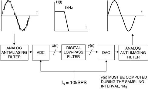
Figure 16.4 Digital filter
The required cut-off frequency of both filters is 1 kHz. The analog filter is realized as a 6-pole Chebyshev Type 1 filter (ripple in pass-band, no ripple in stop-band), and the response is shown in Figure 16.5. In practice, this filter would probably be realized using three 2-pole stages, each of which requires an op-amp, and several resistors and capacitors. Modern filter design CAD packages make the 6-pole design relatively straightforward, but maintaining the 0.5 dB ripple specification requires accurate component selection and matching.
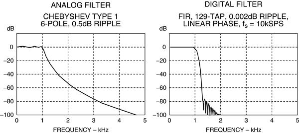
Figure 16.5 Analog vs. digital filter frequency response comparison
On the other hand, the 129-tap digital FIR filter shown has only 0.002 dB pass-band ripple, linear phase, and a much sharper roll-off. In fact, it could not be realized using analog techniques. Another obvious advantage is that the digital filter requires no component matching, and it is not sensitive to drift since the clock frequencies are crystal controlled. The 129-tap filter requires 129 multiply-accumulates (MAC) in order to compute an output sample. This processing must be completed within the sampling interval, 1/fs, in order to maintain real-time operation. In this example, the sampling frequency is 10 kSPS; therefore 100 μs is available for processing, assuming no significant additional overhead requirement. The ADSP-21xx family of DSPs can complete the entire multiply-accumulate process (and other functions necessary for the filter) in a single instruction cycle. Therefore, a 129-tap filter requires that the instruction rate be greater than 129/100 μs = 1.3 million instructions per second (MIPS). DSPs are available with instruction rates much greater than this, so the DSP certainly is not the limiting factor in this application. The ADSP-218x 16-bit fixed-point series offers instruction rates up to 75 MIPS.
The assembly language code to implement the filter on the ADSP-21xx family of DSPs is shown in Figure 16.6. Note that the actual lines of operating code have been marked with arrows; the rest are comments.

Figure 16.6 ADSP-21xx FIR filter assembly code (single precision)
In a practical application, there are certainly many other factors to consider when evaluating analog versus digital filters, or analog versus digital signal processing in general. Most modern signal processing systems use a combination of analog and digital techniques in order to accomplish the desired function and take advantage of the best of both the analog and the digital worlds.
Digital filtering is one of the most powerful tools of DSP. Apart from the obvious advantages of virtually eliminating errors in the filter associated with passive component fluctuations over time and temperature, op-amp drift (active filters), and other effects, digital filters are capable of performance specifications that would, at best, be extremely difficult, if not impossible, to achieve with an analog implementation. In addition, the characteristics of a digital filter can easily be changed under software control. Therefore, they are widely used in adaptive filtering applications in communications such as echo cancellation in modems, noise cancellation, and speech recognition.
The actual procedure for designing digital filters has the same fundamental elements as that for analog filters. First, the desired filter responses are characterized, and the filter parameters are then calculated. Characteristics such as amplitude and phase response are derived in the same way. The key difference between analog and digital filters is that instead of calculating resistor, capacitor, and inductor values for an analog filter, coefficient values are calculated for a digital filter. So for the digital filter, numbers replace the physical resistor and capacitor components of the analog filter. These numbers reside in a memory as filter coefficients and are used with the sampled data values from the ADC to perform the filter calculations.
The real-time digital filter, because it is a discrete time function, works with digitized data as opposed to a continuous waveform, and a new data point is acquired each sampling period. Because of this discrete nature, data samples are referenced as numbers such as sample 1, sample 2, and sample 3. Figure 16.7 shows a low frequency signal containing higher frequency noise which must be filtered out. This waveform must be digitized with an ADC to produce samples x(n). These data values are fed to the digital filter, which in this case is a low-pass filter. The output data samples, y(n), are used to reconstruct an analog waveform using a low glitch DAC.
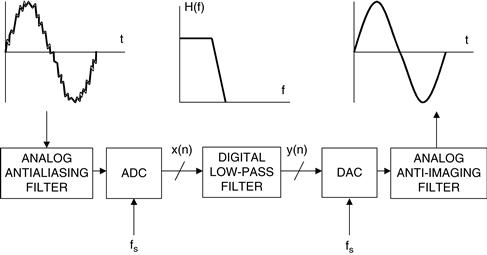
Figure 16.7 Digital filtering
Digital filters, however, are not the answer to all signal processing filtering requirements. In order to maintain real-time operation, the DSP processor must be able to execute all the steps in the filter routine within one sampling clock period, 1/fs. A fast general-purpose fixed-point DSP (such as the ADSP-2189M at 75 MIPS) can execute a complete filter tap multiply-accumulate instruction in 13.3 ns. The ADSP-2189M requires N + 5 instructions for an N-tap filter. For a 100-tap filter, the total execution time is approximately 1.4 μs. This corresponds to a maximum possible sampling frequency of 714 kHz, thereby limiting the upper signal bandwidth to a few hundred kHz.
However, it is possible to replace a general-purpose DSP chip and design special hardware digital filters that will operate at video-speed sampling rates. In other cases, the speed limitations can be overcome by first storing the high speed ADC data in a buffer memory. The buffer memory is then read at a rate that is compatible with the speed of the DSP-based digital filter. In this manner, pseudo-real-time operation can be maintained as in a radar system, where signal processing is typically done on bursts of data collected after each transmitted pulse.
Another option is to use a third-party dedicated DSP filter engine like the Systolix PulseDSP filter core. The AD7725 16-bit sigma-delta ADC has an on-chip PulseDSP filter that can do 125 million multiply-accumulates per second.
Even in highly oversampled sampled data systems, an analog antialiasing filter is still required ahead of the ADC and a reconstruction (anti-imaging) filter after the DAC. Finally, as signal frequencies increase sufficiently, they surpass the capabilities of available ADCs, and digital filtering then becomes impossible. Active analog filtering is not possible at extremely high frequencies because of op-amp bandwidth and distortion limitations, and filtering requirements must then be met using purely passive components. The primary focus of the following discussions will be on filters that can run in real-time under DSP program control.
As an example, consider the comparison between an analog and a digital filter shown in Figure 16.9. The cut-off frequency of both filters is 1 kHz. The analog filter is realized as a 6-pole Chebyshev Type 1 filter (ripple in pass-band, no ripple in stop-band). In practice, this filter would probably be realized using three 2-pole stages, each of which requires an op-amp, and several resistors and capacitors. The 6-pole design is certainly not trivial, and maintaining the 0.5 dB ripple specification requires accurate component selection and matching.
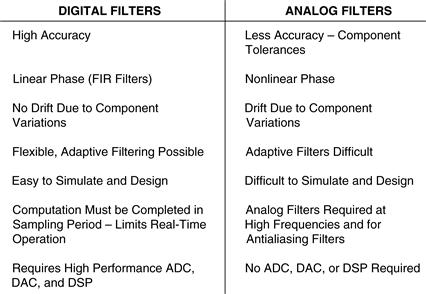
Figure 16.8 Digital vs. analog filtering
On the other hand, the digital FIR filter shown has only 0.002 dB pass-band ripple, linear phase, and a much sharper roll-off. In fact, it could not be realized using analog techniques. In a practical application, there are many other factors to consider when evaluating analog versus digital filters. Most modern signal processing systems use a combination of analog and digital techniques in order to accomplish the desired function and take advantage of the best of both the analog and the digital world.

Figure 16.9 Analog vs. digital filter frequency response comparison
There are many applications where digital filters must operate in real-time. This places specific requirements on the DSP, depending upon the sampling frequency and the filter complexity. The key point is that the DSP must finish all computations during the sampling period so it will be ready to process the next data sample. Assume that the analog signal bandwidth to be processed is fa. This requires the ADC sampling frequency fs to be at least 2fa. The sampling period is 1/fs. All DSP filter computations (including overhead) must be completed during this interval. The computation time depends on the number of taps in the filter and the speed and efficiency of the DSP. Each tap on the filter requires one multiplication and one addition (multiply-accumulate). DSPs are generally optimized to perform fast multiply-accumulates, and many DSPs have additional features such as circular buffering and zero-overhead looping to minimize the “overhead” instructions that otherwise would be needed.

Figure 16.10 Processing requirements for real-time digital filtering
16.7 Finite Impulse Response (FIR) Filters
There are two fundamental types of digital filters: finite impulse response (FIR) and infinite impulse response (IIR). As the terminology suggests, these classifications refer to the filter’s impulse response. By varying the weight of the coefficients and the number of filter taps, virtually any frequency response characteristic can be realized with a FIR filter. As has been shown, FIR filters can achieve performance levels that are not possible with analog filter techniques (such as perfect linear phase response). However, high performance FIR filters generally require a large number of multiply-accumulates and therefore require fast and efficient DSPs. On the other hand, IIR filters tend to mimic the performance of traditional analog filters and make use of feedback, so their impulse response extends over an infinite period of time. Because of feedback, IIR filters can be implemented with fewer coefficients than for a FIR filter. Lattice filters are simply another way to implement either FIR or IIR filters and are often used in speech processing applications. Finally, digital filters lend themselves to adaptive filtering applications simply because of the speed and ease with which the filter characteristics can be changed by varying the filter coefficients.

Figure 16.11 Types of digital filters
The most elementary form of a FIR filter is a moving average filter as shown in Figure 16.12. Moving average filters are popular for smoothing data, such as in the analysis of stock prices. The input samples, x(n) are passed through a series of buffer registers (labeled z−1, corresponding to the z-transform representation of a delay element). In the example shown, there are four taps corresponding to a 4-point moving average. Each sample is multiplied by 0.25, and these results are added to yield the final moving average output y(n). The figure also shows the general equation of a moving average filter with N taps. Note again that N refers to the number of filter taps, and not the ADC or DAC resolution as in previous sections.

Figure 16.12 4-point moving average filter
Since the coefficients are equal, an easier way to perform a moving average filter is shown in Figure 16.13. Note that the first step is to store the first four samples, x(0), x(1), x(2), x(3) in a register. These quantities are added and then multiplied by 0.25 to yield the first output, y(3). Note that the initial outputs y(0), y(1), and y(2) are not valid because all registers are not full until sample x(3) is received.
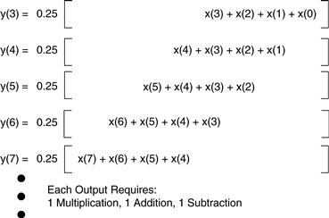
Figure 16.13 Calculating output of 4-point moving average filter
When sample x(4) is received, it is added to the result, and sample x(0) is subtracted from the result. The new result must then be multiplied by 0.25. Therefore, the calculations required to produce a new output consist of one addition, one subtraction, and one multiplication, regardless of the length of the moving average filter.
The step function response of a 4-point moving average filter is shown in Figure 16.14. Notice that the moving average filter has no overshoot. This makes it useful in signal processing applications where random white noise must be filtered but pulse response preserved. Of all the possible linear filters that could be used, the moving average produces the lowest noise for a given edge sharpness. This is illustrated in Figure 16.15, where the noise level becomes lower as the number of taps are increased. Notice that the 0% to 100% rise time of the pulse response is equal to the total number of taps in the filter multiplied by the sampling period.

Figure 16.14 4-tap moving average filter step response

Figure 16.15 Moving average filter response to noise superimposed on step input
The frequency response of the simple moving average filter is sin(x)/x and is shown on a linear amplitude scale in Figure 16.16. Adding more taps to the filter sharpens the roll-off, but does not significantly reduce the amplitude of the sidelobes which are approximately 14 dB down for the 11- and 31-tap filter. These filters are definitely not suitable where high stop-band attenuation is required.

Figure 16.16 Moving average filter frequency response
It is possible to dramatically improve the performance of the simple FIR moving average filter by properly selecting the individual weights or coefficients rather than giving them equal weight. The sharpness of the roll-off can be improved by adding more stages (taps), and the stop-band attenuation characteristics can be improved by properly selecting the filter coefficients. Note that unlike the moving average filter, one multiply-accumulate cycle is now required per tap for the generalized FIR filter. The essence of FIR filter design is the appropriate selection of the filter coefficients and the number of taps to realize the desired transfer function H(f). Various algorithms are available to translate the frequency response H(f) into a set of FIR coefficients. Most of this software is commercially available and can be run on PCs. The key theorem of FIR filter design is that the coefficients h(n) of the FIR filter are simply the quantized values of the impulse response of the frequency transfer function H(f). Conversely, the impulse response is the discrete Fourier transform of H(f).
The generalized form of an N-tap FIR filter is shown in Figure 16.17. As has been discussed, an FIR filter must perform the following convolution equation:

where h(k) is the filter coefficient array and x(n-k) is the input data array to the filter. The number N, in the equation, represents the number of taps of the filter and relates to the filter performance as has been discussed above. An N-tap FIR filter requires N multiply-accumulate cycles.

Figure 16.17 N-tap finite impulse response (FIR) filter
FIR filter diagrams are often simplified as shown in Figure 16.18. The summations are represented by arrows pointing into the dots, and the multiplications are indicated by placing the h(k) coefficients next to the arrows on the lines. The z−1 delay element is often shown by placing the label above or next to the appropriate line.
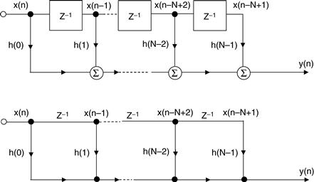
Figure 16.18 Simplified filter notations
16.8 FIR Filter Implementation in DSP Hardware Using Circular Buffering
In the series of FIR filter equations, the N coefficient locations are always accessed sequentially from h(0) to h(N−1). The associated data points circulate through the memory; new samples are added, replacing the oldest each time a filter output is computed. A fixed-boundary RAM can be used to achieve this circulating buffer effect as shown in Figure 16.19 for a four-tap FIR filter. The oldest data sample is replaced by the newest after each convolution. A “time history” of the four most recent data samples is always stored in RAM.

Figure 16.19 Calculating outputs of 4-tap FIR filter using a circular buffer
To facilitate memory addressing, old data values are read from memory starting with the value one location after the value that was just written. For example, x(4) is written into memory location 0, and data values are then read from locations 1, 2, 3, and 0. This example can be expanded to accommodate any number of taps. By addressing data memory locations in this manner, the address generator need only supply sequential addresses, regardless of whether the operation is a memory read or write. This data memory buffer is called circular because when the last location is reached, the memory pointer is reset to the beginning of the buffer.
The coefficients are fetched simultaneously with the data. Due to the addressing scheme chosen, the oldest data sample is fetched first. Therefore, the last coefficient must be fetched first. The coefficients can be stored backward in memory: h(N−1) is the first location, and h(0) is the last, with the address generator providing incremental addresses. Alternatively, coefficients can be stored in a normal manner with the accessing of coefficients starting at the end of the buffer, and the address generator being decremented. In the example shown in Figure 16.19, the coefficients are stored in a reverse manner.
A simple summary flowchart for these operations is shown in Figure 16.20. For Analog Devices DSPs, all operations within the filter loop are completed in one instruction cycle, thereby greatly increasing efficiency. This is referred to as zero-overhead looping. The actual FIR filter assembly code for the ADSP-21xx family of fixed-point DSPs is shown in Figure 16.21. The arrows in the diagram point to the actual executable instructions, and the rest of the code are simply comments added for clarification.

Figure 16.20 Pseudocode for FIR filter program using a DSP with circular buffering

Figure 16.21 ADSP-21xx FIR filter assembly code (single precision)
The first instruction (labeled fir:) sets up the computation by clearing the MR register and loading the MX0 and MY0 registers with the first data and coefficient values from data and program memory. The multiply-accumulate with dual data fetch in the convolution loop is then executed N−1 times in N cycles to compute the sum of the first N−1 products. The final multiply-accumulate instruction is performed with the rounding mode enabled to round the result to the upper 24 bits of the MR register. The MR1 register is then conditionally saturated to its most positive or negative value, based on the status of the overflow flag contained in the MV register. In this manner, results are accumulated to the full 40-bit precision of the MR register, with saturation of the output only if the final result overflowed beyond the least significant 32 bits of the MR register.
The limit on the number of filter taps attainable for a real-time implementation of the FIR filter subroutine is primarily determined by the processor cycle time, the sampling rate, and the number of other computations required. The FIR subroutine presented here requires a total of N + 5 cycles for a filter of length N. For the ADSP-2189M 75 MIPS DSP, one instruction cycle is 13.3 ns, so a 100-tap filter would require 13.3 ns × 100 + 5 × 13.3 ns = 1330 ns + 66.5 ns = 1396.5 ns = 1.4 μs.
16.9 Designing FIR Filters
FIR filters are relatively easy to design using modern CAD tools. Figure 16.22 summarizes the characteristics of FIR filters as well as the most popular design techniques. The fundamental concept of FIR filter design is that the filter frequency response is determined by the impulse response, and the quantized impulse response and the filter coefficients are identical. This can be understood by examining Figure 16.23. The input to the FIR filter is an impulse, and as the impulse propagates through the delay elements, the filter output is identical to the filter coefficients. The FIR filter design process therefore consists of determining the impulse response from the desired frequency response, and then quantizing the impulse response to generate the filter coefficients.

Figure 16.22 Characteristics of FIR filters

Figure 16.23 FIR filter impulse response determines the filter coefficients
It is useful to digress for a moment and examine the relationship between the time domain and the frequency domain to better understand the principles behind digital filters such as the FIR filter. In a sampled data system, a convolution operation can be carried out by performing a series of multiply-accumulates. The convolution operation in the time or frequency domain is equivalent to point-by-point multiplication in the opposite domain. For example, convolution in the time domain is equivalent to multiplication in the frequency domain. This is shown graphically in Figure 16.24. It can be seen that filtering in the frequency domain can be accomplished by multiplying all frequency components in the pass-band by a 1 and all frequencies in the stop-band by 0. Conversely, convolution in the frequency domain is equivalent to point-by-point multiplication in the time domain.

Figure 16.24 Duality of time and frequency
The transfer function in the frequency domain (either a 1 or a 0) can be translated to the time domain by the discrete Fourier transform (in practice, the fast Fourier transform is used). This transformation produces an impulse response in the time domain. Since the multiplication in the frequency domain (signal spectrum times the transfer function) is equivalent to convolution in the time domain (signal convolved with impulse response), the signal can be filtered by convolving it with the impulse response. The FIR filter is exactly this process. Since it is a sampled data system, the signal and the impulse response are quantized in time and amplitude, yielding discrete samples. The discrete samples comprising the desired impulse response are the FIR filter coefficients.
The mathematics involved in filter design (analog or digital) generally make use of transforms. In continuous-time systems, the Laplace transform can be considered to be a generalization of the Fourier transform. In a similar manner, it is possible to generalize the Fourier transform for discrete-time sampled data systems, resulting in what is commonly referred to as the z-transform. Details describing the use of the z-transform in digital filter design are given in References 1 through 6, but the theory is not necessary for the rest of this discussion.
16.9.1 FIR Filter Design Using the Windowed-Sinc Method
An ideal low-pass filter frequency response is shown in Figure 16.25(A). The corresponding impulse response in the time domain is shown in Figure 16.25(B), and follows the sin(x)/x (sinc) function. If a FIR filter is used to implement this frequency response, an infinite number of taps are required. The windowed-sinc method is used to implement the filter as follows. First, the impulse response is truncated to a reasonable number of N taps as in Figure 16.25(C). The frequency response corresponding to Figure 16.25(C) has relatively poor sidelobe performance because of the end-point discontinuities in the truncated impulse response. The next step in the design process is to apply an appropriate window function as shown in Figure 16.25(D) to the truncated impulse. This forces the endpoints to zero. The particular window function chosen determines the roll-off and sidelobe performance of the filter. There are several good choices of window function, depending upon the desired frequency response. The frequency response of the truncated and windowed-sinc impulse response of Figure 16.25(E) is shown in Figure 16.25(F).

Figure 16.25 FIR filter design using the windowed-sinc method
16.9.2 FIR Filter Design Using the Fourier Series Method with Windowing
The Fourier series with windowing method (Figure 16.26) starts by defining the transfer function H(f) mathematically and expanding it in a Fourier series. The Fourier series coefficients define the impulse response and therefore the coefficients of the FIR filter. However, the impulse response must be truncated and windowed as in the previous method. After truncation and windowing, an FFT is used to generate the corresponding frequency response. The frequency response can be modified by choosing different window functions, although precise control of the stop-band characteristics is difficult in any method that uses windowing.
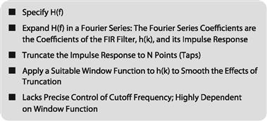
Figure 16.26 FIR Filter design using Fourier series method with windowing
16.9.3 FIR Filter Design Using the Frequency Sampling Method
This method is extremely useful in generating an FIR filter with an arbitrary frequency response. H(f) is specified as a series of amplitude and phase points in the frequency domain. The points are then converted into real and imaginary components. Next, the impulse response is obtained by taking the complex inverse FFT of the frequency response. The impulse response is then truncated to N points, and a window function is applied to minimize the effects of truncation. The filter design should then be tested by taking its FFT and evaluating the frequency response. Several iterations may be required to achieve the desired response.

Figure 16.27 Frequency sampling method for FIR filters with arbitrary frequency response
16.9.4 FIR Filter Design Using the Parks-McClellan Program
Historically, the design method based on the use of windows to truncate the impulse response and to obtain the desired frequency response was the first method used for designing FIR filters. The frequency-sampling method was developed in the 1970s and is still popular where the frequency response is an arbitrary function.
Modern CAD programs are available today that greatly simplify the design of lowpass, high-pass, band-pass, or band-stop FIR filters. A popular one was developed by Parks and McClellan and uses the Remez exchange algorithm. The filter design begins by specifying the parameters shown in Figure 16.28: pass-band ripple, stop-band ripple (same as attenuation), and the transition region. For this design example, the QED1000 program from Momentum Data Systems was used (a demo version is free and downloadable from http://www.mds.com).

Figure 16.28 FIR CAD Techniques: Parks-McClellan program with Remez exchange algorithm

Figure 16.29 Parks-McClellan equiripple FIR filter design: program inputs

Figure 16.30 FIR filter program outputs
For this example, we will design an audio low-pass filter that operates at a sampling rate of 44.1 kHz. The filter is specified as shown in Figure 16.28: 18 kHz pass-band frequency, 21 kHz stop-band frequency, 0.01 dB pass-band ripple, 96 dB stop-band ripple (attenuation). We must also specify the word length of the coefficients, which in this case is 16 bits, assuming a 16-bit fixed-point DSP is to be used.
The program allows us to choose between a window-based design or the equiripple Parks-McClellan program. We will choose the latter. The program now estimates the number of taps required to implement the filter based on the above specifications. In this case, it is 69 taps. At this point, we can accept this and proceed with the design or decrease the number of taps and see what degradation in specifications occur.
We will accept this number and let the program complete the calculations. The program outputs the frequency response (Figure 16.31), step function response (Figure 16.32), s- and z-plane analysis data, and the impulse response (Figure 16.33). The QED1000 program then outputs the quantized filter coefficients to a program that generates the actual DSP assembly code for a number of popular DSPs, including Analog Devices. The program is quite flexible and allows the user to perform a number of scenarios to optimize the filter design.

Figure 16.31 FIR design example: frequency response

Figure 16.32 FIR filter design example: step response
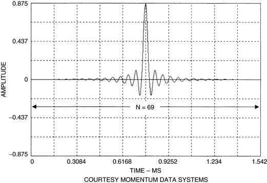
Figure 16.33 FIR design example: impulse response (filter coefficients)
The 69-tap FIR filter requires 69 + 5 = 74 instruction cycles using the ADSP-2189M 75 MIPS processor, which yields a total computation time per sample of 74 × 13.3 ns = 984 ns. The sampling interval is 1/44.1 kHz, or 22.7 μs. This allows 22.7 μs − 0.984 μs = 21.7 μs for overhead and other operations.
Other options are to use a slower processor (3.3 MIPS) for this application, a more complex filter that takes more computation time (up to N = 1700), or increase the sampling frequency to about 1 MSPS.

Figure 16.34 Design example using ADSP-2189M: processor time for 69-tap FIR filter
16.9.5 Designing High-Pass, Band-Pass, and Band-Stop Filters Based on Low-Pass Filter Design
Converting a low-pass filter design impulse response into a high-pass filter impulse response can be accomplished in one of two ways. In the spectral inversion method, the sign of each filter coefficient in the low-pass filter impulse response is changed. Next, 1 is added to the center coefficient. In the spectral reversal method, the sign of every other coefficient is changed. This reverses the frequency domain plot. In other words, if the cut-off of the low-pass filter is 0.2 fs, the resulting high-pass filter will have a cut-off frequency of 0.5 fs − 0.2 fs = 0.3 fs. This must be considered when doing the original low-pass filter design.
Band-pass and band-stop filters can be designed by combining individual low-pass and high-pass filters in the proper manner. Band-pass filters are designed by placing the low-pass and high-pass filters in cascade. The equivalent impulse response of the cascaded filters is then obtained by convolving the two individual impulse responses.
A band-stop filter is designed by connecting the low-pass and high-pass filters in parallel and adding their outputs. The equivalent impulse response is then obtained by adding the two individual impulse responses.

Figure 16.35 Designing high-pass filters using low-pass filter impulse response

Figure 16.36 Band-pass and band-stop filters designed from low-pass and high-pass filters
16.10 Infinite Impulse Response (IIR) Filters
As was mentioned previously, FIR filters have no real analog counterparts, the closest analogy being the weighted moving average. In addition, FIR filters have only zeros and no poles. On the other hand, IIR filters have traditional analog counterparts (Butterworth, Chebyshev, Elliptic, and Bessel) and can be analyzed and synthesized using more familiar traditional filter design techniques.
Infinite impulse response filters get their name because their impulse response extends for an infinite period of time. This is because they are recursive, i.e., they utilize feedback. Although they can be implemented with fewer computations than FIR filters, IIR filters do not match the performance achievable with FIR filters, and do not have linear phase. Also, there is no computational advantage achieved when the output of an IIR filter is decimated, because each output value must always be calculated.
IIR filters are generally implemented in 2-pole sections called biquads because they are described with a biquadratic equation in the z-domain. Higher order filters are designed using cascaded biquad sections, e.g., a 6-pole filter requires three biquad sections.

Figure 16.37 Infinite impulse response (IIR) filters
The basic IIR biquad is shown in Figure 16.38. The zeros are formed by the feed-forward coefficients b0, b1, and b2; the poles are formed by the feedback coefficients a1, and a2.

Figure 16.38 Hardware implementation of second-order IIR filter (biquad) Direct Form 1
The general digital filter equation is shown in Figure 16.38, which gives rise to the general transfer function H(z), which contains polynomials in both the numerator and the denominator. The roots of the denominator determine the pole locations of the filter, and the roots of the numerator determine the zero locations. Although it is possible to construct a high order IIR filter directly from this equation (called the direct form implementation), accumulation errors due to quantization errors (finite word-length arithmetic) may give rise to instability and large errors. For this reason, it is common to cascade several biquad sections with appropriate coefficients rather than use the direct form implementation. The biquads can be scaled separately and then cascaded in order to minimize the coefficient quantization and the recursive accumulation errors. Cascaded biquads execute more slowly than their direct form counterparts, but are more stable and minimize the effects of errors due to finite arithmetic errors.
The Direct Form 1 biquad section shown in Figure 16.38 requires four registers. This configuration can be changed into an equivalent circuit shown in Figure 16.39 that is called the Direct Form 2 and requires only two registers. It can be shown that the equations describing the Direct Form 2 IIR biquad filter are the same as those for Direct Form 1. As in the case of FIR filters, the notation for an IIR filter is often simplified as shown in Figure 16.40.

Figure 16.39 IIR biquad filter Direct Form 2

Figure 16.40 IIR biquad filter simplified notations
16.11 IIR Filter Design Techniques
A popular method for IIR filter design is to first design the analog-equivalent filter and then mathematically transform the transfer function H(s) into the z-domain, H(z). Multiple pole designs are implemented using cascaded biquad sections. The most popular analog filters are the Butterworth, Chebyshev, Elliptical, and Bessel (see Figure 16.41). There are many CAD programs available to generate the Laplace transform, H(s), for these filters.
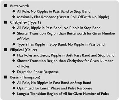
Figure 16.41 Review of popular analog filters
The all-pole Butterworth (also called maximally flat) has no ripple in the pass-band or stop-band and has monotonic response in both regions. The all-pole Type 1 Chebyshev filter has a faster roll-off than the Butterworth (for the same number of poles) and has ripple in the pass-band. The Type 2 Chebyschev filter is rarely used, but has ripple in the stop-band rather than the pass-band.
The Elliptical (Cauer) filter has poles and zeros and ripple in both the pass-band and stop-band. This filter has even faster roll-off than the Chebyshev for the same number of poles. The Elliptical filter is often used where degraded phase response can be tolerated.
Finally, the Bessel (Thompson) filter is an all-pole filter optimized for pulse response and linear phase but has the poorest roll-off of any of the types discussed for the same number of poles.
All of the above types of analog filters are covered in the literature, and their Laplace transforms, H(s), are readily available, either from tables or CAD programs. There are three methods used to convert the Laplace transform into the z-transform: impulse invariant transformation, bilinear transformation, and the matched z-transform. The resulting z-transforms can be converted into the coefficients of the IIR biquad. These techniques are highly mathematically intensive and will not be discussed further.
A CAD approach for IIR filter design is similar to the Parks-McClellan program used for FIR filters. This technique uses the Fletcher-Powell algorithm.
In calculating the throughput time of a particular DSP IIR filter, one should examine the benchmark performance specification for a biquad filter section. For the ADSP21xx family, seven instruction cycles are required to execute a biquad filter output sample. For the ADSP-2189M, 75 MIPS DSP, this corresponds to 7 × 13.3 ns = 93 ns, corresponding to a maximum possible sampling frequency of 10 MSPS (neglecting overhead).

Figure 16.42 IIR filter design techniques

Figure 16.43 Throughput considerations for IIR filters
16.11.1 Summary: FIR Versus IIR Filters
Choosing between FIR and IIR filter designs can be somewhat of a challenge, but a few basic guidelines can be given. Typically, IIR filters are more efficient than FIR filters because they require less memory and fewer multiply-accumulates are needed. IIR filters can be designed based upon previous experience with analog filter designs. IIR filters may exhibit instability problems, but this is much less likely to occur if higher order filters are designed by cascading second-order systems.

Figure 16.44 Comparison between FIR and IIR filters
On the other hand, FIR filters require more taps and multiply-accumulates for a given cut-off frequency response, but have linear phase characteristics. Since FIR filters operate on a finite history of data, if some data is corrupted (ADC sparkle codes, for example) the FIR filter will ring for only N−1 samples. Because of the feedback, however, an IIR filter will ring for a considerably longer period of time.
If sharp cut-off filters are needed, and processing time is at a premium, IIR elliptic filters are a good choice. If the number of multiply/accumulates is not prohibitive, and linear phase is a requirement, the FIR should be chosen.
16.12 Multirate Filters
There are many applications in which it is desirable to change the effective sampling rate in a sampled data system. In many cases, this can be accomplished simply by changing the sampling frequency to the ADC or DAC. However, it is often desirable to accomplish the sample rate conversion after the signal has been digitized. The most common techniques used are decimation (reducing the sampling rate by a factor of M), and interpolation (increasing the sampling rate by a factor of L). The decimation and interpolation factors (M and L) are normally integer numbers. In a generalized sample-rate converter, it may be desirable to change the sampling frequency by a noninteger number. In the case of converting the CD sampling frequency of 44.1 kHz to the digital audio tape (DAT) sampling rate of 48 kHz, interpolating by L = 160 followed by decimation by M = 147 accomplishes the desired result.
The concept of decimation is illustrated in Figure 16.45. The top diagram shows the original signal, fa, which is sampled at a frequency fs. The corresponding frequency spectrum shows that the sampling frequency is much higher than required to preserve information contained in fa, i.e., fa is oversampled. Notice that there is no information contained between the frequencies fa and fs − fa. The bottom diagram shows the same signal where the sampling frequency has been reduced (decimated) by a factor of M. Notice that even though the sampling rate has been reduced, there is no aliasing and loss of information. Decimation by a larger factor than shown in Figure 16.45 will cause aliasing.

Figure 16.45 Decimation of a sampled signal by a factor of M
Figure 16.46(A) shows how to decimate the output of an FIR filter. The filtered data y(n) is stored in a data register that is clocked at the decimated frequency fs/M. This does not change the number of computations required of the digital filter; i.e., it still must calculate each output sample y(n).

Figure 16.46 Decimation combined with FIR filtering
Figure 16.46(B) shows a method for increasing the computational efficiency of the FIR filter by a factor of M. The data from the delay registers are simply stored in N data registers that are clocked at the decimated frequency fs/M. The FIR multiply-accumulates now only have to be done every Mth clock cycle. This increase in efficiency could be utilized by adding more taps to the FIR filter, doing other computations in the extra time, or using a slower DSP.
Figure 16.47 shows the concept of interpolation. The original signal in 16.47(A) is sampled at a frequency fs. In 16.47(B), the sampling frequency has been increased by a factor of L, and zeros have been added to fill in the extra samples. The signal with added zeros is passed through an interpolation filter, which provides the extra data values.

Figure 16.47 Interpolation by a factor of L
The frequency domain effects of interpolation are shown in Figure 16.48. The original signal is sampled at a frequency fs and is shown in 16.48(A). The interpolated signal in 16.48(B) is sampled at a frequency Lfs. An example of interpolation is a CD player DAC, where the CD data is generated at a frequency of 44.1 kHz. If this data is passed directly to a DAC, the frequency spectrum shown in Figure 16.48(A) results, and the requirements on the anti-imaging filter that precedes the DAC are extremely stringent to overcome this. An oversampling interpolating DAC is normally used, and the spectrum shown in Figure 16.48(B) results. Notice that the requirements on the analog anti-imaging filter are now easier to realize. This is important in maintaining relatively linear phase and also reducing the cost of the filter.

Figure 16.48 Effects of interpolation on frequency spectrum
The digital implementation of interpolation is shown in Figure 16.49. The original signal x(n) is first passed through a rate expander that increases the sampling frequency by a factor of L and inserts the extra zeros. The data then passes through an interpolation filter that smoothes the data and interpolates between the original data points. The efficiency of this filter can be improved by using a filter algorithm that takes advantage of the fact that the zero-value input samples do not require multiply-accumulates. Using a DSP that allows circular buffering and zero-overhead looping also improves efficiency.

Figure 16.49 Typical interpolation implementation
Interpolators and decimators can be combined to perform fractional sample rate conversion as shown in Figure 16.50. The input signal x(n) is first interpolated by a factor of L and then decimated by a factor of M. The resulting output sample rate is Lfs/M. To maintain the maximum possible bandwidth in the intermediate signal, the interpolation must come before the decimation; otherwise, some of the desired frequency content in the original signal would be filtered out by the decimator.

Figure 16.50 Sample rate converters
An example is converting from the CD sampling rate of 44.1 kHz to the digital audio tape (DAT) sampling rate of 48.0 kHz. The interpolation factor is 160, and the decimation factor, 147. In practice, the interpolating filter h′ (k) and the decimating′ filter h′′(k) are combined into a single filter, h(k).
The entire sample rate conversion function is integrated into the AD1890, AD1891, AD1892, and AD1893 family, which operates at frequencies between 8 kHz and 56 kHz (48 kHz for the AD1892). The AD1895 and AD1896 operate at up to 192 kHz.
16.13 Adaptive Filters
Unlike analog filters, the characteristics of digital filters can easily be changed by modifying the filter coefficients. This makes digital filters attractive in communications applications such as adaptive equalization, echo cancellation, noise reduction, speech analysis, and speech synthesis. The basic concept of an adaptive filter is shown in Figure 16.51. The objective is to filter the input signal, x(n), with an adaptive filter in such a manner that it matches the desired signal, d(n). The desired signal, d(n), is subtracted from the filtered signal, y(n), to generate an error signal. The error signal drives an adaptive algorithm that generates the filter coefficients in a manner that minimizes the error signal. The least mean square (LMS) or recursive least square (RLS) algorithms are two of the most popular.

Figure 16.51 Adaptive filter
Adaptive filters are widely used in communications to perform such functions as equalization, echo cancellation, noise cancellation, and speech compression. Figure 16.52 shows an application of an adaptive filter used to compensate for the effects of amplitude and phase distortion in the transmission channel. The filter coefficients are determined during a training sequence where a known data pattern is transmitted. The adaptive algorithm adjusts the filter coefficients to force the receive data to match the training sequence data. In a modem application, the training sequence occurs after the initial connection is made. After the training sequence is completed, the switches are put in the other position, and the actual data is transmitted. During this time, the error signal is generated by subtracting the input from the output of the adaptive filter.
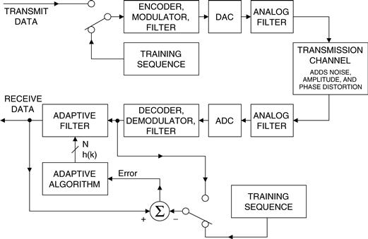
Figure 16.52 Digital transmission using adaptive equalization
Speech compression and synthesis also makes extensive use of adaptive filtering to reduce data rates. The linear predictive coding (LPC) model shown in Figure 16.53 models the vocal tract as a variable frequency impulse generator (for voiced portions of speech) and a random noise generator (for unvoiced portions of speech such as consonant sounds). These two generators drive a digital filter that in turn generates the actual voice signal.
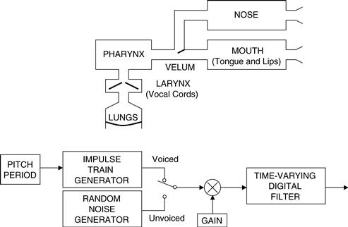
Figure 16.53 Linear predictive coding (LPC) model of speech production
The application of LPC in a communication system such as GSM is shown in Figure 16.54. The speech input is first digitized by a 16-bit ADC at a sampling frequency of 8 kSPS. This produces output data at 128 Kbps, which is much too high to be transmitted directly. The transmitting DSP uses the LPC algorithm to break the speech signal into digital filter coefficients and pitch. This is done in 20 ms windows, which have been found to be optimum for most speech applications. The actual transmitted data is only 2.4 Kbps, which represents a 53.3 compression factor. The receiving DSP uses the LPC model to reconstruct the speech from the coefficients and the excitation data. The final output data rate of 128 Kbps then drives a 16-bit DAC for final reconstruction of the speech data.

Figure 16.54 LPC Speech companding system
The digital filters used in LPC speech applications can either be FIR or IIR, although all-pole IIR filters are the most widely used. Both FIR and IIR filters can be implemented in a lattice structure as shown in Figure 16.55 for a recursive all-pole filter. This structure can be derived from the IIR structure, but the advantage of the lattice filter is that the coefficients are more directly related to the outputs of algorithms that use the vocal tract model shown in Figure 16.53 than the coefficients of the equivalent IIR filter.
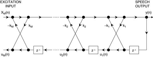
Figure 16.55 All-pole lattice filter
The parameters of the all-pole lattice filter model are determined from the speech samples by means of linear prediction as shown in Figure 16.56. Due to the nonstationary nature of speech signals, this model is applied to short segments (typically 20 ms) of the speech signal. A new set of parameters is usually determined for each time segment unless there are sharp discontinuities, in which case the data may be smoothed between segments.

Figure 16.56 Estimation of lattice filter coefficients in transmitting DSP
References
1. Practical Design Techniques for Sensor Signal Conditioning. Analog Devices 1998.
2. Sheingold Daniel H, ed. Transducer Interfacing Handbook Analog Devices, Inc. 1972.
3. Higgins Richard J. Digital Signal Processing in VLSI Prentice-Hall 1990.
4. Smith Steven W. Digital Signal Processing: A Guide for Engineers and Scientists Newnes 2002.
5. Britton Rorabaugh C. DSP Primer McGraw-Hill 1999.
6. Higgins Richard J. Digital Signal Processing in VLSI Prentice-Hall 1990.
7. Oppenheim AV, Schafer RW. Digital Signal Processing Prentice-Hall 1975.
8. Rabiner LR, Gold B. Theory and Application of Digital Signal Processing Prentice-Hall 1975.
9. Proakis John G, Manolakis Dimitris G. Introduction to Digital Signal Processing MacMillian 1988.
10. McClellan JH, Parks TW, Rabiner LR. A Computer Program for Designing Optimum FIR Linear Phase Digital Filters. IEEE Trasactions on Audio and Electroacoustics. December, 1973;Vol. AU-21.
11. Harris Fredrick J. On the Use of Windows for Harmonic Analysis with the Discrete Fourier Transform. Proc IEEE. 1978;Vol. 66(No. 1):51–83.
12. Momentum Data Systems, Inc. 17330 Brookhurst St., Suite 140, Fountain Valley, CA 92708, http://www.mds.com.
13. Digital Signal Processing Applications Using the ADSP-2100 Family, Vol. 1 and Vol. 2, Analog Devices, Free Download at: http://www.analog.com.
14. ADSP-21000 Family Application Handbook, Vol. 1, Analog Devices, Free Download at: http://www.analog.com.
15. Widrow B, Stearns SD. Adaptive Signal Processing Prentice-Hall 1985.
16. Haykin S. Adaptive Filter Theory. 3rd Prentice-Hall 1996.
17. Honig Michael L, Messerschmitt David G. Adaptive Filters — Structures, Algorithms, and Applications Hingham, MA: Kluwer Academic Publishers; 1984.
18. Markel JD, Gray Jr AH. Linear Prediction of Speech New York, NY: Springer-Verlag; 1976.
19. Rabiner LR, Schafer RW. Digital Processing of Speech Signals Prentice-Hall 1978.