
Chapter 15
Interfacing
15.1 Mixing Analog and Digital
The two main problems that face designers who have to integrate analog and digital circuits on the same PCB are:
• preventing digital switching noise from contaminating the analog signal, and
• interfacing the wide range of analog input voltages to the digital circuit.
Generating analog outputs from digital signals is not usually a problem. Generating digital inputs from analog signals is.
15.1.1 Ground Noise
The high-frequency switching noise that was discussed earlier must be kept out of analog circuits at all costs. An analog-to-digital interface quantizes a variable analog signal into a digital word, and the number of bits in the word determines the resolution that can be achieved of the signal. Assuming a full-scale voltage range of 0 to 10V, which is typical of many analog-digital converters (ADCs), Table 15.1 shows the voltage levels that correspond to one bit change in the digital word.
Table 15.1 ADC resolution voltage for different word lengths, 10V full-scale
| Word length | Resolution voltage |
| 8 bit | 39 mV |
| 10 bit | 10 mV |
| 12 bit | 2.4 mV |
| 14 bit | 0.6 mV |
| 16 bit | 0.15 mV |
You can see that the more resolution is demanded of the interface, the smaller the voltage change that will cause one bit change. 8 bits is regarded as commonplace in ADC circuits, 12 bits as reasonably high resolution (0.025%) and 16 bits as precision.
The significance of these diminishing voltage levels is that any noise that is coupled into the analog input will cause unwanted fluctuation of the digital value. For a 12-bit converter, a one-bit uncertainty will be given by noise of 2.4 mV at the converter input; for a 16-bit, this reduces to 150 microvolts. By contrast, the switching noise on the digital ground line is normally tens of millivolts and frequently hundreds of millivolts peak amplitude. If this noise were coupled into the converter input—and it is hard to keep ground noise out of the input—you would be unable to use a converter of greater precision than 8-10 bits.
15.1.2 Filtering
One partial solution to this problem is to filter the bandwidth of the analog signal to well below that of the noise so that the effective noise signal is reduced. For slowly varying analog signals this works reasonably well, especially if the noise injection occurs at the input of the signal-processing amplifier so that bandwidth limitation has maximum effect. Filtering is in any case good practice to minimize susceptibility to external noise.
Filtering the input amplifier is no use if the noise is injected into the ADC itself. For fast ADCs and wide-bandwidth analog signals you cannot take this approach anyway and the only available solution is to prevent the injection of digital noise at its source.
15.1.3 Segregation
The basic rule to follow when designing an analog-to-digital interface is to segregate the circuits, including grounds, completely. This means that:
• separate analog and digital grounds should be established, connected only at one point, and
• the analog and digital sections of the circuit should be physically separated, with no digital tracks traversing the analog section, or vice versa. This will minimize crosstalk between the circuits.
It should be appreciated that no grounding scheme that establishes a multiplicity of different grounds can ever be optimum, because there will always be circuits that need to communicate signals across different ground areas. These signals are then particularly exposed to the nuances of both internal and external interference, or indeed may be the source of it. You should always strive to make such circuits low-risk in terms of their bandwidth and sensitivity, or else keep a single ground system for all circuits (both digital and analog) and take extreme care in its layout so that ground noise from one noisy part of the system does not circulate in another sensitive part.
15.1.4 Single-Board Systems
The appropriate grounding schemes for single-board and multi-board systems are shown in Figure 15.1. If your system has a single analog-to-digital converter, perhaps with a multiplexer to select from several analog inputs, then the connection between analog and digital grounds can be made at this ADC as in Figure 15.1(A). This scheme requires that the analog and digital power supply returns are not linked together anywhere else, so that two separate power supply circuits are needed. The analog and digital grounds must be treated as entirely separate tracks, despite being nominally at the same potential; unavoidable noise currents circulating in the digital ground will then not couple into the “clean” analog ground. The digital ground should be of gridded or ground plane construction, whereas the analog section may benefit from a single-point grounding system, or may have a separate ground plane of its own. On no account should you extend the digital ground plane over the analog section of the board, since there will then be capacitive coupling from one ground plane to another.
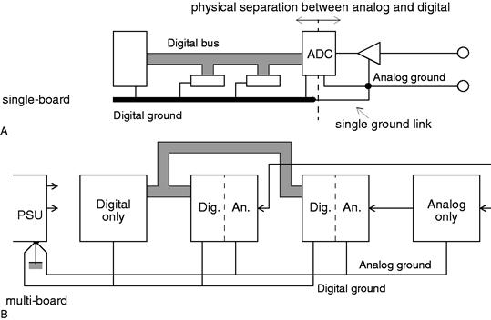
Figure 15.1 Layout for separate analog and digital grounds
15.1.5 Multi-Board Systems
When your system consists of several boards, some entirely digital, some entirely analog and some a mixture of the two, with an external power supply, then you cannot make the connection between digital and analog grounds at the ADC. There may be several ADCs in the one system. Instead, make the link at the power supply (Figure 15.1 (B)) and run separate analog and digital grounds to each board that requires them. Digital-only boards should be located physically closer to the power supply to minimize the radiating loop area or length.
15.2 Generating Digital Levels from Analog Inputs
The first rule when you want to use a varying analog voltage to generate an on/off digital signal—as distinct from an analog-to-digital conversion—is: always use either a comparator or a Schmitt-trigger gate. Never feed an analog signal straight into an ordinary TTL or CMOS gate input.
The reason is that ordinary gates do not have well-defined input voltage switching thresholds. Not only that, but they are also very critical of slow rise-time inputs. Very few analog input signals have the slew rate, typically faster than 5 V/μs, required to produce a clean output from an ordinary logic gate. The result of applying a slow analog voltage to a logic gate is shown in Figure 15.2.

Figure 15.2 The effect of a slow input to a logic gate
A Schmitt trigger gate, or a comparator with hysteresis, will get over the slow rise time problem. A Schmitt trigger gate has the same output characteristics as an ordinary gate but it includes input hysteresis to ensure a fast transition. The threshold levels of typical Schmitt devices, such as the 74HC14, are specified within wide tolerances and so do not overcome the variability of the actual switching point. When the analog levels corresponding to high and low states can be kept above VIH and below VIL, respectively, a Schmitt is adequate. For more precision you will need to use a comparator with an accurately specified reference voltage.
Second, if the analog supply rail range is greater than the logic supply, interfacing the analog signal straight to the logic input will threaten the gate with damage. This is possible even if the normal signal range is within the logic supply range; abnormal conditions such as turn-on or turn-off may exceed the rails. This, of course, is also a problem with Schmitt trigger gates. Normally, the inputs are protected by clamp diodes to the supply and ground rails, but the current through these must be limited to a safe level so a resistor in series with the input is essential. More positive steps to limit the input voltage, such as running the analog section from the same supply voltage as the logic (heeding the earlier advice about separate digital and analog ground rails), are to be preferred.
15.2.1 DebBouncing Switch Inputs
On the face of it, switch inputs to digital circuitry must be the easiest of interfaces. All you should need are an input port or gate, a pull-up resistor and a single pole switch (Figure 15.3). This circuit, though it undoubtedly works, is prone to a serious problem because of the electromechanical nature of the switch and the speed of logic devices.

Figure 15.3 Contact bounce
When a switch contact operates, the current flow is not cleanly initiated or interrupted. As the contacts come together or part, the instantaneous contact resistance varies due to contamination, and the mating surfaces may “bounce” apart a few times due to the springiness of the material. As a result the switching edge is irregular and may easily consist of several discrete edges, extending over a period of typically 1 ms. You can verify this behavior simply by observing the input waveform of Figure 15.3 on a storage scope.
Of course, the digital input responds very fast to each crossing of the switching threshold, and consequently the port or gate sees several transitions each time the switch is operated, before it settles to a steady-state 1 or 0. This may not be a problem for level-sensitive inputs, but it undoubtedly is for edge-sensitive ones such as counter or latch clock inputs. Mistriggering of counter circuits that are fed from a switch input is commonly caused by this phenomenon.
The simple solution to contact bounce is to filter the logic input with an RC network (Figure 15.4(A)). The RC time constant must be significantly longer than the bounce period to effectively attenuate the contact noise. This has the extra advantage of protecting against induced impulsive or RF interference, but it requires additional discrete components and demands that the logic input must be a Schmitt-trigger type, since the input rise time has been deliberately slowed.

Figure 15.4 Switch debouncing circuits
If the switch input may change state quickly, an RC time constant that is sufficiently long to cure the bounce will slow the response to the switch unacceptably. This can be overcome in two ways: the RS latch, Figure 15.4(B), which requires a changeover rather than single-throw switch, or a software- or hardware-implemented delay. Figure 15.4(C) shows the hardware delay, which uses a continuously clocked shift register and OR gate to effectively “window out” the bounce. The delay can be adjusted to suit the bounce period. These two solutions are most suited to realization with semicustom logic arrays or ASICs, where the overhead of the extra logic is low.
15.3 Protection Against Externally Applied Overvoltages
Logic inputs and outputs which are taken off-board will be subject at some time in the life of the system to an overvoltage. Your philosophy in this respect should be: if it can happen, it will. Overvoltages can be applied by misconnection of the board or of external equipment, or can be due to static build-up. The latter is a particular threat to CMOS inputs with their high impedance, but the effect of a large static discharge can also be disastrous for other logic families.
There are three major consequences of an overvoltage on a logic signal line:
• immediate damage of the device due to rupture of the track metallization or destruction of the silicon;
• progressive degradation of device characteristics when the overvoltage does not have enough energy to destroy it immediately;
• latch-up, where damage may be caused by excessive power supply current following a transient overvoltage.
Modern logic families include some protection both at their inputs and outputs in the form of clamping diodes to the supply lines, but these diodes are limited in their current-handling ability and therefore the potential fault current that can be applied due to an overvoltage must be limited. This is best achieved by the methods of Figure 15.5.
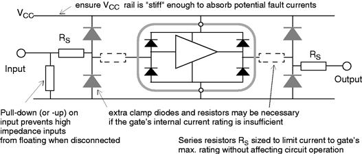
Figure 15.5 Logic gate I/O protection
The external clamp diodes are used to take the lion’s share of the incoming overload current and divert it to the VCC or 0V rails; the resistors shown dotted are needed if the IC’s internal diodes would otherwise still take too much current because of the ratio of their forward voltage to the external diodes’ forward voltages. The power rail takes the excess incoming current and must therefore be of a low enough impedance for its voltage to be substantially unaffected by this current being dumped into it. This may call for a review of the regulator philosophy, or for extra clamps to be applied on the power rail local to the interfaces. Series resistors RS may be adequate in themselves without external clamp diodes, especially on inputs, where they can be used to limit the current to what can be handled by the IC’s internal diodes.
15.4 Isolation
Even if you take precautions against input/output abuse, it is not good practice to take logic signals directly into or out of equipment. As well as facing the threat of overload on individual lines, you also have to extend the ground and/or supply rails outside the equipment to provide a signal return path. These then act as antennas both to radiate ground noise out of the equipment and to conduct external interference back into it. It is very much safer to keep power rails within the bounds of the equipment case.
A common technique to achieve this is to electrically isolate all signal lines entering or leaving the equipment. As well as guarding against interference, this eliminates problems from ground loops and ground differentials. Digital signals lend themselves to the use of opto-couplers. An opto-coupler is basically an LED chip integrated in the same package as a light-sensitive device such as a photodiode or phototransistor, the two components being electrically separate but optically coupled. A typical isolation scheme using such devices is shown in Figure 15.6.

Figure 15.6 Interface isolation using opto-couplers
One opto-coupler is needed per digital channel. Opto-couplers can be sourced as single, dual or quad packages, and the price for commercial grade units can vary depending mainly on the required speed and level of integration from 25p to £5 per channel. Clearly, in cost- or space-sensitive applications the number of isolated channels should be minimized. This tends to mean that isolation is more common in industrial products than consumer ones.
15.4.1 Opto-Coupler Trade-Offs
There are a number of quite complex trade-offs to make when you use opto-isolation. Factors to consider are:
• Speed of the interface: cheap couplers with standard transistor outputs have switching times of 2–5 μs so are limited to data rates of around 100 kbits/s maximum. High speed devices with data rates of 10 Mbits/s are available but cost over £5 per channel.
• Power consumption: standard transistor output types offer a current transfer ratio (CTR) typically between 10 and 80%. This is the ratio of LED input current to transistor output current in the on-state. Thus for a required output current of 1 mA with a CTR of 20%, 5 mA would be needed through the LED. Also, CTR degrades with time and you should include an extra safety margin of between 20 and 50%, depending on expected lifetime and operating current, to ensure end-of-life circuit reliability. Reducing the operating current reduces the speed of the interface. Darlington-output optocouplers are available with CTRs of 200–500%, but these unfortunately have turn-off times of around 100 μs so are only useful for low-speed purposes. Opto-coupler drive current can be a significant fraction of the overall power requirement, especially on the isolated side.
• Support circuitry: a simple photo-transistor or photo-Darlington output needs several passive components plus a buffer gate to interface it correctly to logic levels. Alternatively, you can get opto-couplers which have logic-compatible inputs and outputs, especially the faster ones, but at a significantly higher cost. Low-current LED drive requirements can be met directly by a logic gate and series limiting resistor, whereas if you are using a cheaper opto with higher LED current you will need an extra buffer.
15.4.2 Coupling Capacitance
Although an opto-coupler breaks the electrical connection at DC, with an isolation voltage measured in kV, there is still some residual coupling capacitance which reduces the isolation at high frequencies. The specification figures of 0.5–2 pF are increased somewhat by stray wiring capacitance which is layout dependent. Input and output pins are invariably on opposite sides of the package. There is no point in designing in an opto-coupler for isolation if you then run the output tracks back alongside the input tracks!
The coupling capacitance of individual channels, multiplied by the number of channels in the system, means that a significant level of high frequency ground noise may still be coupled out of an isolated system, or fast rise time transients or RFI may still be coupled in. (This is another argument for minimizing the number of channels.) Also, high common mode dV/dt signals can be coupled directly into the photodiode or transistor input through this capacitance and cause false switching. This effect is reduced by incorporating an electrostatic screen across the optical path and connecting it to the output ground pin, and some opto-couplers are available with this screen included. Common mode transient immunity can vary from worse than 100 V/μs to better than 5 kV/μs (for the expensive devices).
15.4.3 Alternatives to Opto-Couplers
Two alternatives to opto-couplers for isolating digital signals are relays and pulse transformers. The relay is a well-established device and is a good choice if its restrictions of size, weight, speed, power consumption and electromechanical nature are acceptable.
Pulse transformers are most useful for passing wide bandwidth, high speed digital data for which opto-couplers are too slow or too expensive. They can also be designed for good immunity to high dV/dt interference. The data must be coded or modulated to remove any DC component. This requires an overhead of a few gates and a latch per channel, but this overhead may be acceptable, especially if you are already using semicustom silicon, and may easily be outweighed by the attractions of high speed and low power consumption.
15.5 Classic Data Interface Standards
When you want to connect logic signals from one piece of equipment to another, it is not sufficient to use standard logic devices and make direct gate-to-gate connections, even if they are isolated from the main system. Standard logic is not suited to driving long lines; line terminations are unspecified and noise immunity is low, so that reflections and interference would give unacceptably high data corruption. External logic interfaces must be specially designed for the purpose.
At the same time, it is essential that there is some commonality of interface between different manufacturers’ equipment. This allows the user to connect, say, a computer from manufacturer A to a printer from manufacturer B without worrying about electrical compatibility. There is therefore a need for a standard definition for electrical interface signals. This need has been recognized for many years, and there are a wide variety of data interchange standards available. The logic of the marketplace has dictated that only a small number of these are dominant. This section will consider the two main commercial ones: EIA-232F and EIA-422. EIA-232F is an update of the popular RS-232C standard published in 1969, to bring it into line with the international CCITT V.24 and V.28 and ISO IS2110 standards. EIA-422 is the same as the earlier RS-422 standard. The prefix changes are cosmetic, purely to identify the source of the standards as the EIA.
15.5.1 EIA-232F
The boom in data communications has led to many products which make interface conformity claims by quoting “RS-232” in their specifications. Some of these claims are in fact quite spurious, and discerning users will regard interface conformity as an indicator of product quality, and test it early on in their evaluation. The major characteristics of the specification are given in Table 15.2. As well as specifying the electrical parameters, EIA-232F also defines the mechanical connections and pin configuration, and the functional description of each data circuit.
Table 15.2 Major electrical characteristics of EIA

By modern standards the performance of EIA-232F is primitive. It was originally designed to link data terminal equipment (DTE) to modems, known as data communications equipment (DCE). It was also used for data terminal-to-mainframe interfaces. These early applications were relatively low speed, less than 20 kbaud, and used cables shorter than 50 feet. Applications which call for such limited capability are now abundant, hence the standard’s great popularity. Its new revision recognizes this by replacing the phrase “data communication equipment” with “data circuit-terminating equipment,” also abbreviated to DCE. It does not clarify exactly what is a DTE and what is a DCE, and since many applications are simple DTE (computer) to DTE (terminal or printer) connections, it is often open to debate as to what is at which end of the interface. Although a point-to-point connection provides the correct pin terminations for DTE-to-DCE, a useful extra gadget is a cable known as a null modem (Figure 15.7), which creates a DTE-to-DTE connection. The common sight of an installation technician crouched over a 9-way connector swapping pins 2 and 3, to make one end’s receiver listen to the other end’s driver, has yet to disappear.

Figure 15.7 The null modem
EIA-232F’s transmission distance is limited by its unbalanced design and restricted drive current. The unbalanced design is very susceptible to external noise pick-up and to ground shifts between the driver and receiver. The limited drive current means that the slew rate must be kept slow enough to prevent the cable becoming a transmission line, and this puts a limit on the fastest data rate that can be accommodated. Maximum cable length, originally fixed at 50 feet, is now restricted by a requirement for maximum load capacitance (including receiver input) for each circuit of 2500 pF. As the line length increases so does its capacitance, requiring more current to maintain the same transition time. The graph of Figure 15.8 shows the drive current versus load capacitance required to maintain the 4% transition time relationship at different data rates. In practice, the line length is limited to 3 meters or less for data rates more than 20 kb/s. Most drivers can handle the higher transmission rates over such a short length without drawing excessive supply current.

Figure 15.8 EIA-232F transmit driver output current versus CL
Note that there are several common “enhancements” that are not permitted by strict adherence to the standard. EIA-232F makes no provision for tristating the driver output, so multiple driver access to one line is not possible. Similarly, paralleling receivers is not allowed unless the combined input impedance is held between 3 kΩ and 7 kΩ. It does not consider electrically isolated interfaces: no specification is offered for isolation requirements, despite their desirability. It does not specify the communication data format. The usual “one start bit, eight data bits, two stop bits” format is not part of the standard, just its most common application. It is not directly compatible with another common single-ended standard, EIA-423, although such connections will usually work. Also, you cannot legitimately run EIA-232F off a ±5V supply rail—the minimum driver output voltage is specified as ±5V, loaded with 3–7 kΩ and with an output impedance of 300Ω.
The standard calls for slew-rate limiting to 30 V/μs maximum. Although you can do this with an output capacitor, which operates in conjunction with the output transistor’s current limit while it is slewing, this will increase the dissipation, and reduces the maximum possible cable length. It is preferable to use a driver that has on-chip slew rate limiting, requiring no external capacitors and making the slew rate independent of cable length.
15.5.2 EIA-422
Many data communications applications now require data rates in the megabaud region, for which EIA-232F is inadequate. This need is fulfilled by the EIA-422 standard, which is an electrical specification for drivers and receivers for use in a balanced or differential, point-to-point or multi-drop high speed interface using twisted pair cable. Table 15.2 summarizes the EIA-422 specification in comparison with EIA-232F. One driver and up to ten receivers are allowed. The maximum data rate is specified as 10 Mbaud, with a trade-off against cable length; maximum cable length at 100 kbaud is 4000 feet. Note that unlike EIA-232F, EIA-422 does not specify functional or mechanical parameters of the interface. These are included in other standards which incorporate it, notably EIA-449 and EIA-530.
EIA-422 achieves its high-speed and long-distance capabilities by specifying a balanced and terminated design. The balanced design reduces sensitivity to external common mode noise and allows a ground differential of up to a few volts to exist between the driver and one or more of the receivers without affecting the receiver’s thresholds. A cable termination, together with increased driver current, allows fast slew rates which in turn allows high data rates. If the cable is not terminated, serious ringing on the edges occurs which may cause spurious switching in the receiver. The specified termination of 100Ω is closely matched to the characteristic impedance of typical twisted pair cables. Only one termination is used, at the receiver at the far end of the cable.
15.5.3 Interface Design
By far the easiest way to realize either EIA-232F or EIA-422 interfaces is to use one of the many specially tailored driver and receiver chip sets that are available. The more common ones, such as the 1488 driver/1489 receiver for EIA-232F or the 26LS31 driver/26LS32 receiver for EIA-422, are available competitively from many sources and in low-power CMOS versions. You can also obtain combined driver/receiver parts so that a small interface can be handled with one IC. Because the 9-pin implementation of EIA-232F is so common, a single package 3-transmitter plus 5-receiver part is also widely sourced. The high-voltage requirement of EIA-232F, typically ±12V supplies, is addressed by some suppliers who offer on-chip DC-to-DC converters from the =5V rail.
Figure 15.9 suggests typical interface circuits for the two standards. Note the inclusion of power supply isolating diodes, to protect the rest of the circuit against the inevitable overvoltages that will come its way. You can also construct an interface, particularly the simpler EIA-232F, using standard components such as op-amps, comparators, CMOS buffer devices or discrete components if you are prepared to spend some time characterizing the circuit against the requirements of the standard and against expected overload conditions. This may turn out to be marginally cheaper in component cost, but its overall worth is somewhat questionable.

Figure 15.9 Typical EIA-232F and EIA-422 interface circuits
15.6 High Performance Data Interface Standards
This section briefly reviews some of the newer data interface standards that have grown up for high-speed purposes around particular applications and have subsequently become more widely entrenched.
15.6.1 EIA-485
EIA-485 shares many similarities with EIA-422, and is widely used as the basis for inhouse and industrial datacomm systems. For instance, one variant of the SCSI interface (HVD-SCSI: high voltage differential—small computer systems interface) uses 485 as the basis for its electrical specification. 485-compliant devices can be used in 422 systems, though the reverse is not necessarily true. The principal difference is that 485 allows multiple transmitters on the same line, driving up to 32 unit loads, with halfduplex (bidirectional) communication. One unit load is defined as a steady-state load allowing 1 mA of current under a maximum common mode voltage of 12V or 0.8 mA at −7V. ULs may consist of drivers or receivers and failsafe resistors (see below), but do not include the termination resistors. The bidirectional communication means that 485 drivers must allow for line contention and for driving a line that is terminated at each end with 120Ω. The two specifications are compared in Table 15.2.
One further problem that arises in a half-duplex system is that there will be periods when no transmitters are driving the line, so that it becomes high impedance, and it is desirable for the receivers to remain in a fixed state in this situation. This means that a differential voltage of more than 200 mV should be provided by a suitable passive circuit that complies with both the termination impedance requirements and the unit load constraints. A network designed to do this is called a “failsafe” network.
15.6.2 CAN
The Controller Area Network (CAN) standard was originally developed within the automotive industry to replace the complex electrical wiring harness with a two-wire data bus. It has since been standardized in ISO 11898. The specification allows signaling rates up to 1 MB/s, high immunity from electrical interference, and an ability to self-diagnose and repair errors. It is now widespread in many sectors, including factory automation, medical, marine, aerospace and of course automotive. It is particularly suited to applications requiring many short messages in a short period of time with high reliability in noisy operating environments.
The ISO 11898 architecture defines the lowest two layers of the OSI/ISO seven layer model, that is, the data-link layer and the physical layer. The communication protocol is carrier-sense multiple access, with collision detection and arbitration on message priority (CSMA/CD=AMP). The first version of CAN was defined in ISO 11519 and allowed applications up to 125 kB/s with an 11-bit message identifier. The 1 MB/s ISO 11898:1993 version is standard CAN 2.0A, also with an 11-bit identifier, while Extended CAN 2.0B is provided in a 1995 amendment to the standard and provides a 29-bit identifier.
The physical CAN bus is a single twisted pair, shielded or unshielded, terminated at each end with 120Ω. Balanced differential signaling is used. Nodes may be added or removed at any time, even while the network is operating. Un-powered nodes should not disturb the bus, so transceivers should be configured so that their pins are in a high impedance state with the power off. The standard specification allows a maximum cable length of 40m with up to 30 nodes, and a maximum stub length (from the bus to the node) of 0.3m. Longer stub and line lengths can be implemented, with a trade-off in signaling rates. The recessive (quiescent) state is for both bus lines to be biased equally to approximately 2.5V relative to ground; in the dominant state, one line (CANH) is taken positive by 1V while the other (CANL) is taken negative by the same amount, giving a 2V differential signal. The required common mode voltage range is from −2V to =7V, i.e., ±4.5V about the quiescent state.
15.6.3 USB
The Universal Serial Bus (USB) is a cable bus that supports data exchange between a host computer and a wide range of simultaneously accessible peripherals. The attached peripherals share USB bandwidth through a host scheduled, token-based protocol.
The bus allows peripherals to be attached, configured, used, and detached while the host and other peripherals are in operation. There is only one host in any USB system. The USB interface to the host computer system is referred to as the Host Controller, which may be implemented in a combination of hardware, firmware, or software.
USB devices are either hubs, which act as wiring concentrators and provide additional attachment points to the bus, or system functions such as mice, storage devices or data sources or outputs. A root hub is integrated within the host system to provide one or more attachment points.
The USB transfers signal and power over a four-wire point-to-point cable. A differential input receiver must be used to accept the USB data signal. The receiver has an input sensitivity of at least 200 mV when both differential data inputs are within the common mode range of 0.8V to 2.5V. A differential output driver drives the USB data signal with a static output swing in its low state of <0.3V with a 1.5 kΩ load to 3.6V and in its high state of >2.8V with a 15 kΩ load to ground. A full-speed USB connection is made through a shielded, twisted pair cable with a characteristic impedance (Z0) of 90Ω 15% and a maximum one-way delay of 26 ns. The impedance of each of the drivers must be between 28 and 44Ω. The detailed specification controls the rise and fall times of the output drivers for a range of load capacitances.
In version 1.1, there are two data rates:
• the full-speed signaling bit rate is 12 Mb/s;
• a limited capability low-speed signaling mode is also defined at 1.5 Mb/s.
Both modes can be supported in the same USB bus by automatic dynamic mode switching between transfers. The low-speed mode is defined to support a limited number of low-bandwidth devices, such as mice. In order to provide guaranteed input voltage levels and proper termination impedance, biased terminations are used at each end of the cable. The terminations also allow detection of attachment at each port and differentiate between full-speed and low-speed devices. The USB 2.0 specification adds a high-speed data rate of 480 MB/s between compliant devices using the same cable as 1.1, with both source and load terminations of 45Ω.
The cable also carries supply wires, nominally =5V, on each segment to deliver power to devices. Cable segments of variable lengths, up to several meters, are possible. The specification defines connectors, and the cable has four conductors: a twisted signal pair of standard gauge and a power pair in a range of permitted gauges.
The clock is transmitted, encoded along with the differential data. The clock encoding scheme is nonreturn-to-zero with bit stuffing to ensure adequate transitions. A SYNC field precedes each packet to allow the receiver(s) to synchronize their bit recovery clocks.
15.6.4 Ethernet
Ethernet is a well-established specification for serial data transmission. It was first published in 1980 by a multivendor consortium that created the DEC-Intel-Xerox (DIX) standard. In 1985, Ethernet was standardized in IEEE 802.3; since that time it has been extended a number of times. “Classic” Ethernet operates at a data transmission rate of 10 Mbit/s. Since the 1990s, Ethernet has developed in the following areas:
Nowadays, Ethernet is the most widespread networking technology in the world in commercial information technology systems, and is also gaining importance in industrial automation. All network users have the same rights under Ethernet. Any user can exchange data of any size with another user at any time, and any network device that is transmitting is heard by all other users. Each Ethernet user filters the data packets that are intended for it out from the stream, ignoring all the others.
In the standard Ethernet, all the network users share one collision domain. Network access is controlled by the CSMA/CD procedure (carrier sense multiple access with collision detection). Before transmitting data, a network user first checks whether the network is free (carrier sense). If so, it starts to transmit data. At the same time it checks whether other users have also begun to transmit (collision detection). If that is the case, a collision occurs. All the network users concerned now stop their transmission, wait for a period of time determined according to a randomizing principle, and then start transmission again. The result of this is that the time required to transmit data packets depends heavily on the network loading, and cannot be determined in advance. The more collisions occur, the slower the entire network becomes.
This lack of determinism can be overcome by a variant of the basic approach known as switched Ethernet. This refers to a network in which each Ethernet user is assigned a port in a switch, which analyzes all the data packets as they arrive, directing them on to the appropriate port. Switches separate former collision domains into individual point-to-point connections between the network components and the relevant user equipment. Preventing collisions makes the full network bandwidth available to each point-to-point connection. The second pair of conductors in the four-wire Ethernet cable, which otherwise is needed for collision detection, can now be used for transmission, so providing a significant increase in data transfer rate.
The Ethernet interface at each user is defined according to Figure 15.10. It is usual to find structured twisted pair local area network wiring already integrated within a building, and the cabling characteristics are given in IEC 11801 and related standards; hence the 10Base-T and 100Base-T variants are the most popular of the Ethernet implementations, and the appropriate MAU/MDI using the RJ45 connector are included in most types of computer. The maximum lengths are set by signal timing limitations in the Fast Ethernet implementation, and an Ethernet system implementation relies on correct integration of cable lengths, types and terminations.

Figure 15.10 Ethernet interface and media
In contrast to the coaxial versions of Ethernet, which may be connected in multidrop, each segment of twisted pair or fiber route is a point-to-point connection between hosts; this means that a network system that is more than simply two hosts requires a number of hubs or switches, which integrate the connections to each user. A hub will simply pass through the Ethernet traffic between its ports without controlling it in any way, but a switch does control the traffic, separating packets to their destination ports.
The 100Base-T electrical characteristics are a peak differential output signal of 1V into a 100Ω characteristic impedance twisted pair; the 10Base-T level is 2.5V. The rise and fall time and amplitude symmetries are also defined to achieve a high level of balance and hence common mode performance. It is normal to use a transformer and common mode choke to isolate the network connection from the driver electronics.