
Chapter 14
Designing with Logic ICs
14.1 Logic ICs
The interfaces between logic integrated circuits including signal, clock and power supply lines must be considered to achieve a reliable digital design. This applies whether the devices concerned are microprocessors, their support chips, application specific ICs (ASICs), programmable logic arrays (PLAs) or standard “glue” logic.
14.1.1 Noise Immunity and Thresholds
A logic input can take any value of voltage, nominally from one supply rail to the other, although due to transmission line effects the actual voltage can exceed either supply rail on transitions. Each input is designed so that any voltage below one level, conventionally VIL, is regarded as a logic “0” and any voltage above another level, VIH , is regarded as logic “1” (Figure 14.1).

Figure 14.1 Transitions through logic thresholds
These levels are characterized for each logic or microprocessor family, and worst case values of VIL and VIH can be found on any data sheet. Note that, as with any hardware-determined parameter, they may vary with temperature and you should ensure that the values you use are guaranteed across the device’s temperature range. They are also a function of supply voltage. If all ICs are fed from the same supply this is not a problem, but it becomes more significant if you are interfacing logic circuits which may be fed from different supply rails.
The significance of the band between VIL and VIH is that the input logic state (and therefore the output state) is undefined while the voltage is in this band. Therefore, transitions between logic states must happen as rapidly as possible and no decisions must be taken while the input is in transit, or for a given period (the “settling time”) thereafter. This is why clocked, or synchronous, circuits are normally more reliable than unclocked or asynchronous ones for complex logic operations: the state of the clock determines when logic decisions are taken, and it is arranged that all data transitions occur when the clock is inactive.
14.1.1.1 Susceptibility to Noise
Provided that all signals to logic inputs, whether from other logic outputs or from interfaces to other circuits, lie outside the VIL − VIH band when they are active, then in theory no misinterpretation of the input should occur. The difference between a “low” output logic level (VOL) and VIL, or that between a “high” output level (VOH) and VIH, is the noise immunity (expressed in volts) of the logic interface (Figure 14.2). Notice that noise immunity is not a property of any particular device, but of the interface between devices. The noise immunity of a family of devices (such as LVT or HCMOS) only refers to interfaces between devices of the same family.

Figure 14.2 Noise immunity of a logic interface
14.1.1.2 Current Immunity
The noise immunity value gives meaning to the ability of the interface to withstand externally coupled noise without corruption of the perceived logic level. So for instance the HCMOS-LSTTL interface can tolerate a variation of 2.4V in the high state, or 0.47V in the low state. These are worst-case values and the actual circuit could tolerate somewhat more before a change of state occurred. But the voltage difference is only part of the story. When noise is coupled into an interface, the impedance of the interface is just as important, since this determines what voltage will be developed by a given induced interference current. The impedance is normally defined by the output driver (as long as transmission line effects are neglected) and the effective noise current threshold of the interface, given by the noise immunity voltage divided by the driver output impedance, gives a truer picture of the actual noise immunity of a given combination.
The metal-gate 4000B CMOS logic family has a high output impedance at 5V compared with the other families, so that its current immunity is significantly worse. However, as the supply voltage increases so its output impedance goes down, and the combined effect means that its immunity at 15V VCC is about ten times better than at 5V. It is inherently insensitive to low voltage inductively coupled noise, but shows poor rejection of capacitively coupled noise. For general-purpose 5V applications the 74HC family is preferred. It is also true that a microcontroller’s high output resistance means that it does not compare favorably with standard logic.
14.1.1.3 Use of a Pull-Up
Note that the figures for high-state and low-state immunities are often different, because of the differing drive impedances and voltage thresholds in the two states. A negative immunity value indicates that, if nothing further is done, this particular interface combination will be unreliable by design. For instance, the 2.7V minimum high output of the venerable LS-TTL family is less than the required 3.15V minimum VIH for HCMOS so LS-TTL driving directly into HCMOS is in danger of incorrectly transmitting the logic high level. The standard remedy for this particular situation (if you are still using LS-TTL!) is a pull-up resistor to VCC to ensure a higher output from the LS-TTL (Figure 14.3). The minimum resistor value is a function of the driver output capability, and the maximum value depends on permissible timing constraints. Alternatively, use the HCTMOS family, whose inputs are characterized especially for driving from LS-TTL levels.

Figure 14.3 Logic interface pull-up resistor
14.1.1.4 Dynamic Noise Immunity
The static noise margins as discussed above apply until the interference approaches the operating speed of the devices. When very fast interference is present, higher amplitude is necessary to induce upset. The dynamic noise margin is measured by applying an interference pulse of known magnitude and increasing its width until the device just begins to switch. This yields a plot of noise margin versus pulse width such as shown in Figure 14.4. The high level and low level dynamic noise margins may be different.

Figure 14.4 Dynamic noise immunity of 74HC series devices
You may often be forced to interface different logic families. Typically, a 3.3V microprocessor may need to drive 5V buffers or vice versa, or you may not be able to source a particular part in the same family as the rest of the system, or you may need to change families to optimize speed/power product. You can normally expect logic interfaces of the same family to be compatible, but whenever different families or a custom interface are used you have to check the logic threshold aspects of each one. The voltage level conversion issue is very common, to the extent that there are families of devices such as the 74LVT series which are characterized for an input range of 2.0 VIH and 0.8 VIL, but can still operate from a 5V rail; or vice versa, can accept 5V-swing inputs while being operated from a 3.3V rail.
14.1.2 Fan-Out and Loading
The output voltage levels that are used to fix noise immunity thresholds are not absolute. They depend as usual on temperature, but more importantly on the output current that the driver is required to source or sink. This in turn depends on the type of loading that each output sees (Figure 14.5).

Figure 14.5 Logic output loading
Any driver has an output voltage versus current characteristic which saturates at some level of loading (Figure 14.6). The characteristic is tailored so that at a given load current, the output voltage VOH or VOL is equivalent to the input threshold voltage (VIH or VIL) plus the noise immunity for that particular logic family. This load current then corresponds to the sum of the input currents for a given number N of standard gates of that family, and N is called the fan-out: that number of standard gates that the output can drive and still keep the interface within the noise threshold limits. The fan-out is normally specified against each output of a device for other devices of the same family, but it can be calculated for other logic family interfaces or indeed for any DC load current simply by comparing the output voltage and current capability for each logic state with the current and voltage requirements of each input. As before, fan-out figures for logic high and low may differ.

Figure 14.6 Logic driver output characteristics
For CMOS families there is rarely a limit on the number of inputs that can be driven at DC by one output. When low-power parts are required to drive high-power types, then fan-out may be insufficient and you have to use intermediate buffer devices. The low drive capability of many microprocessor bus outputs severely restricts the number of other components that may be placed on the bus without interposing additional bus buffers—which accounts for the phenomenal popularity of the 74XX244 type of octal bus driver!
14.1.2.1 Dynamic Loading
The DC load current taken by the input side of the interface is only part of the total load. Indeed, for CMOS-input logic ICs it is negligible and has no significant effect on fanout calculations. But every input has an associated capacitance to ground and the charging or discharging of this capacitance limits the speed at which the node can operate. Typical logic IC input capacitances are 5–10 pF and these must be summed for all connected inputs, together with an allowance for interconnection capacitance which is layout-dependent but is again typically 5 pF, to reach the total load capacitance facing the driver.
Driver dynamic output current ability is rarely specified on data sheets but some manufacturers give application guidance. For instance, the 74HC range can offer typically ± 40 mA for standard devices and ± 60 mA for buffers at 4.5V supply. This current slews the interface node capacitance Cn (Figure 14.7) that you have just calculated and you have to ensure that slewing from logic 0 to the logic 1 threshold, or vice versa, is accomplished before the input data level is required to be valid. As an example, a 100 pF capacitance slewing from 0 to 3V with 40 mA drive will take 7.5 ns, and this time (plus a safety factor) has to be added onto the other specified propagation delays to ensure adequate timing margin. If the figures don’t add up, you will need to add extra buffer devices (which add their own propagation delays), reduce the load, reduce the operating frequency or go to a faster logic family.

Figure 14.7 Propagation and slewing delays
If you choose to run CMOS devices with a high load capacitance and accept that the edges will be slower, then be aware that this also reduces the reliability of the device because of the higher transient currents that the output drivers are handling.
14.1.3 Induced Switching Noise
This phenomenon is more colloquially known as ground bounce. We are not talking here about external noise signals, but about noise which is induced on the supply rails by the switching action of each logic gate in the circuit.
As each gate changes state, a current pulse is taken from the supply pins because of the different device currents required in each state, the external loading, the transient caused by charging or discharging the node capacitance, and the conduction overlap in the totem-pole output stage. All these effects are present in all logic families to some extent, although CMOS types suffer little from the first two. In most cases, the node capacitance charging current dominates, more so with higher-speed circuits. The capacitance Cn must be charged with a current of
![]()
Thus a 74AC-series gate with a dV/dt of around 1.6V/ns will require a 50 mA current pulse when charging a 30 pF node capacitance. Figure 14.8 shows the current paths. The significance of the supply current spike is that it causes a disturbance in the supply voltage and also in the ground line, because of the inductive impedance of the lines. A pulse with a di/dt of 50 mA/ns through a track inductance of 20 nH (one inch of track) will generate a voltage pulse of 1V peak, which is approaching the noise margin of fast logic. Supply voltage spikes are not too much of a problem as the logic high level noise immunity is usually good and they can be attenuated by proper decoupling, as the next section shows. Ground line disturbances are more threatening. Pulses on a high-impedance ground line can easily exceed the noise threshold and cause spurious switching of innocent gates. Only if a good, low-inductance ground plane system is maintained can this problem be minimized.
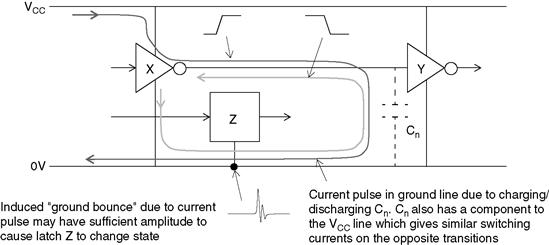
Figure 14.8 Induced ground noise due to switching currents
14.1.3.1 Synchronous Switching
The supply pin pulse current is magnified in synchronous systems when several gates switch simultaneously. A typical example is an octal bus buffer or latch whose data changes from #FFH to #00H. If all outputs are heavily loaded, as may be the case when the device is driving a large data bus, a formidable current pulse—exceeding an amp in fast systems—will pass through the ground pin. Worse, if seven bits of an octal latch change simultaneously, the induced ground bounce may corrupt the state of the eighth bit. You need to ensure that such devices are grounded to their loads with a very low-inductance ground system, preferably a true ground plane.
Ground noise on a microprocessor board can easily be observed by hooking a wide bandwidth oscilloscope to the ground line—you can connect the scope probe tip and its ground together and still see the noise, since the magnetic fields due to the ground currents will induce a signal in the loop formed by the probe leads. What you see is a regular series of narrow, ringing pulses spaced at the clock period. The amplitude of each pulse varies because the sum of the data transitions is random, but the timing does not. Such noise (Figure 14.9) is impossible to remove entirely.
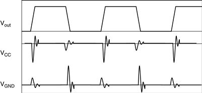
Figure 14.9 Switching noise on power and ground rails
14.1.4 Decoupling
No matter how good the VCC and ground connections are, you cannot eliminate all line inductance. Except on the smallest boards, track distance will introduce an impedance which will create switching noise from the transient currents discussed in the last section. This is the reason for decoupling (Figure 14.10).

Figure 14.10 Logic decoupling scheme
14.1.4.1 Distance
The purpose of a decoupling capacitor is to maintain a low dynamic impedance from the individual IC supply voltage to ground. This minimizes the local supply voltage droop when a fast current pulse is taken from it. The word “decoupling” means isolating the local circuit from the supply impedance. Bearing in mind the speed of the current pulses just discussed, it should be clear that the capacitor must be located close to the circuit it is decoupling. “Close” in this context means less than half an inch for fast logic such as 74AC or ECL, especially when high current devices such as bus drivers are involved, extending to several inches for low-current, slow devices such as 4000B series CMOS.
If the decoupling current path between IC and capacitor is too long, the track inductance in conjunction with the capacitor forms a high-Q LC tuned circuit, and the ringing it generates will have a worse effect than no decoupling at all.
14.1.4.2 Capacitor Type and Value
The crucial factor for high-speed logic decoupling is lead inductance rather than absolute value. Minimum lead inductance offers a low impedance to fast pulses. Small chip capacitors are preferred, and the smaller the better, since this minimizes the package inductance. 0805, 0603 or even 0402 sizes are acceptable.
You can calculate the value if you want to by matching the transient current demand to the acceptable power rail voltage droop. Take for example a 74HC octal buffer, each of whose outputs when switching takes a transient current of 50 mA for 6 ns (calculated from I = Cn · dV/dt). The total peak current demand is then 0.4A.
The acceptable voltage droop is perhaps 0.4V (equivalent to the worst system noise margin). Assume that the local decoupling capacitor supplies all of the current to hold the droop to this level, which is reasonable if other decoupling capacitors on the board are isolated by track inductance. Then the minimum capacitor value is
![]()
On the other hand, the actual value is noncritical, especially as the variables in the above calculation tend to be somewhat vague, and you will prefer to use the same component in all decoupling positions for ease of production. Values between 10 and 100 nF are recommended, a good compromise being 22 nF, which has both low self-inductance and respectable reservoir capacitance. It also tends to be cheaper than the higher values, particularly in the low-performance Z5U or Y5V ceramic grades, which are adequate for this purpose.
14.1.4.3 Capacitors Under the IC Package
Very high-speed and high-current logic ICs push the location requirement of the decoupling capacitor to its limits: it has to be right next to the supply pins. In fact, the inductance of the lead-out wires within the chip package becomes significant, and this has meant that locating power and ground pins in the middle of, or all around, the package rather than at opposite corners is necessary for high-performance large scale ICs. For such devices it is necessary to locate the decoupling capacitors underneath the chip, on the opposite side of the board. The leads to the capacitors are then limited to the vias between the device pads, the planes and the capacitor pads. This is easily achievable with surface mount construction but of course not if you are restricted to through hole.
In fact the power and ground planes themselves are more effective at reducing the high frequency noise than are the decoupling capacitors, because their associated capacitance has no significant inductance. The closer together the planes are, the higher is this capacitance. You still need discrete decoupling capacitors for mid-frequency decoupling but their positioning becomes less important, as long as they are still located close to the relevant IC pins.
14.1.4.4 Low-Frequency Decoupling
You also need to decouple the supply rail against lower-frequency ripple due to varying logic load currents, as distinct from transient switching edges. The frequency of these ripple components is in the megahertz range and lower, so that widely distributed capacitance and low self-inductance are less important. Typically, they can be dealt with by a few tantalum electrolytics of 1–2 μF placed around the board, particularly where there are several devices that can turn on together and produce a significant drain from the power supply, such as burst refresh in dynamic RAM. Additionally, a single large capacitor of 10–47 μF at the power entry to the board is recommended to cope with frequency components in the kHz range.
Under normal circumstances, logic circuits are inherently insensitive to ripple on the supply lines. The exception is when they are faced with slow edges; if the ripple is at a substantially higher frequency than the edge and is modulating the signal, then as the signal passes through the transition region the logic element may undergo spurious switching (Figure 14.11).
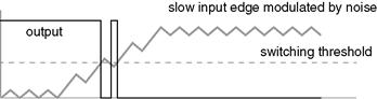
Figure 14.11 Spurious switching on slow edges due to ripple
The safest way to deal with slow edges is to apply hysteresis with a Schmitt-trigger logic input.
14.1.4.5 Guidelines
The minimum requirements for good decoupling are:
• one 22 μF bulk capacitor per board;
• one 1 μF tantalum capacitor per 10 packages of SSI/MSI logic or memory;
• one 1 μF tantalum capacitor per 2–3 LSI packages;
• one 10–100 nF ceramic multilayer capacitor for each supply pin of an LSI package with multiple supply pins;
• one 10–100 nF ceramic multilayer capacitor for each octal IC or for each MSI package; and
• one 10–100 nF ceramic multilayer capacitor per 4 packages of SSI logic.
When in doubt, calculate the requirements for individual power/speed-hungry devices to make sure you have enough capacitors, and that they are in the right places.
14.1.5 Unused Gate Inputs
Frequently you will have spare gates or latches in a package left over, or will not be using all the inputs of a multi-input gate or latch. All such unused logic inputs must be tied to a fixed voltage, either high or low, and should never be left floating. Noise immunity of floating inputs is poor, so you should not float spare inputs of used gates, and especially not preset/clear inputs of latches or flip-flops, which are very sensitive to spikes. Figure 14.12 illustrates the options.

Figure 14.12 Connecting unused inputs
You must connect all unused CMOS inputs either to VCC or ground. Floating any input is inadmissible, whether its gate is used or not. This is because the CMOS input has a very high impedance and consequently can float to any voltage if unconnected, and this voltage could be within the threshold switchover region of the gate. At this point both the P-channel and N-channel input transistors are conducting, which results in excessive current drain through the package. Due to the high gain of buffered gates, it is possible for a gate to oscillate, resulting in even higher current drain.
CMOS inputs can be connected directly to either rail; a protection resistor is unnecessary, as long as the supply is not expected to carry noise spikes that would exceed the maximum input voltage.