
Chapter 5
Transistors Field-Effect
An important milestone in the development of modern active semiconductor devices was the field-effect transistor, or FET for short. These did not become generally available until the 1960s, although they were described in detail and analyzed as early as 1952.
Figure 5.1(A) shows the symbols and Figure 5.1(B) and (C) the construction and operation of the first type introduced, the depletion mode junction FET or JFET. In this device, in contrast to the bipolar transistor, conduction is by means of majority carriers which flow through the channel between the source (analogous to an emitter or cathode) and the drain (collector or anode). The gate is a region of silicon of opposite polarity to the source cum channel cum drain. When the gate is at the same potential as the source and drain, its depletion region is shallow and current carriers (electrons in the case of the N-channel FET shown in Figure 5.1(C)) can flow between the source and the drain. The FET is thus a unipolar device, and minority carriers play no part in its action. As the gate is made progressively more negative, the depletion layer extends across the channel, depleting it of carriers and eventually pinching off the conducting path entirely when Vgs reaches −Vp, the pinch-off voltage. Thus for zero (or only very small) voltages of either polarity between the drain and the source, the device can be used as a passive voltage-controlled resistor. The JFET is, however, more normally employed in the active mode as an amplifier (Figure 5.1(D)) with a positive supply rail (for an N-channel JFET), much like an NPN transistor stage. Figure 5.1(E) shows a typical drain characteristic. Provided that the gate is reversed biased (as it normally will be) it draws no current.
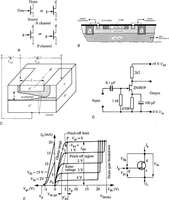
Figure 5.1 Depletion mode junction field-effect transistors. (A) Symbols. (B) Structure of an N-channel JFET. (C) Sectional view of an N-channel JFET. The P+ upper and lower gate regions should be imagined to be connected in front of the plane of the paper, so that the N-channel is surrounded by an annular gate region. (D) JFET audio-frequency amplifier. (E) Characteristics of N-channel JFET: pinch-off voltage Vp = −6V.
(Parts (B), (C) and (E) reproduced by courtesy of Philips Components Ltd.).
The positive excursions of gate voltage of an N-channel JFET, or the negative excursions in the case of a P-channel JFET, must be limited to less than about 0.5V to avoid turn-on of the gate/source junction; otherwise the benefit of a high input impedance is lost.
In the metal-oxide semiconductor field-effect transistor (MOSFET) the gate is isolated from the channel by a thin layer of silicon dioxide, which is a nonconductor; thus, the gate circuit never conducts regardless of its polarity relative to the channel. The channel is a thin layer formed between the substrate and the oxide. In the enhancement (normally off) MOSFET, a channel of semiconductor of the same polarity as the source and drain is induced in the substrate by the voltage applied to the gate (Figure 5.2(B)). In the depletion (normally on) MOSFET, a gate voltage is effectively built in by ions trapped in the gate oxide (Figure 5.2(C)). Figure 5.2(A) shows symbols for the four possible types, and Figure 5.2(D) summarizes the characteristics of N-channel types. Since it is much easier to arrange for positive ions to be trapped in the gate oxide than negative ions or electrons, P-channel depletion MOSFETs are not generally available. Indeed, for both JFETs and MOSFETs of all types, N-channel devices far outnumber P-channel devices. In consequence, one only chooses a P-channel device where it notably simplifies the circuitry or where it is required to operate with an N-channel device as a complementary pair.

Figure 5.2 Metal-oxide semiconductor field-effect transistors. (A) MOSFET types. Substrate terminal b (bulk) is generally connected to the source, often internally. (B) Cross-section through an N-channel enhancement (normally off) MOSFET. (C) Cross-section through an N-channel depletion (normally on) MOSFET. (D) Examples of FET characteristics: (a) normally off (enhancement); (b) normally on (depletion and enhancement); (c) pure depletion (JFETs only).
(Parts (A) to (D) reproduced by courtesy of Philips Components Ltd.).
Note that while the source and substrate are internally connected in many MOSFETS, in some (such as the Motorola 2N351) the substrate connection is brought out on a separate lead. In some instances it is possible to use the substrate, where brought out separately, as another input terminal. For example, in a frequency changer application, the input signal may be applied to the gate and the local oscillator signal to the substrate. In high-power MOSFETS, whether designed for switching applications or as HF/VHF/UHF power amplifiers, the substrate is always internally connected to the source.
In the N-channel dual-gate MOSFET (Figure 5.3) there is a second gate between gate 1 and the drain. Gate 2 is typically operated at +4V with respect to the source and serves the same purpose as the screen grid in a tetrode or pentode. Consequently the reverse transfer capacitance Crss between drain and gate 1 is only about 0.01 pF, against 1 pF or thereabouts for small-signal JFETs, single-gate MOSFETs and most bipolar transistors designed for RF applications.
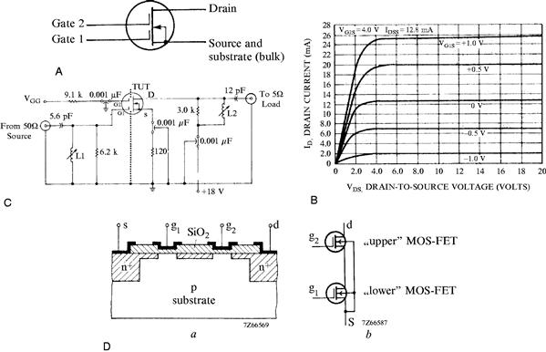
Figure 5.3 Dual-gate MOSFETS. (A) Dual-gate N-channel MOSFET symbol. Gate protection diodes, not shown, are fabricated on the chip in many device types. These limit the gate/source voltage excursion in either polarity, to protect the thin gate oxide layer from excessive voltages, e.g., static charges. (B) Drain characteristics (3N203/MPF203). (C) Amplifier with AGC applied to gate 2.50Ω source and load (3N203/MPF203). (D) Construction and discrete equivalent of a dual-gate N-channel MOSFET.
Parts (B) and (C) reproduced by courtesy of Motorola Inc. Part (D) reproduced by courtesy of Philips Components Ltd.
N-channel power MOSFETs for switching applications are available with drain voltage ratings up to 500V or more and are capable of passing 20A with a drain/source voltage drop of only a few volts, corresponding to a drain/source resistance in the fully on condition of rds on on of just a few hundred milliohms. Other devices with lower drain voltage ratings exhibit rds on resistances as low as 0.010 ohms, and improved devices are constantly being developed and introduced. Consequently these figures will already doubtless be out of date by the time you read this. A very high drain voltage rating in a power MOSFET requires the use of a high-resistivity drain region, so that very low levels of rds on cannot be achieved in high-voltage MOSFETs.
A development which provides a lower drain/source voltage drop in the fully on condition utilizes an additional p-type layer at the drain connection. This is indicated by the arrowhead on the symbol for this type of device (Figure 5.4A). The device is variously known as a conductivity modulated power MOSFET or COMFET (trademark of GE/RCA), as a gain enhanced MOSFET or GEMFET (trademark of Motorola), and so on. Like the basic MOSFET these are all varieties of insulated gate field-effect transistors (IGFETs). The additional heavily doped p-type drain region results in the injection of minority carriers (holes) into the main n-type drain region when the device switches on, supplementing the majority carrier electrons and reducing the drain region on voltage drop. However, nothing comes for free in this world, and the price paid here is a slower switch-off than a pure MOSFET; this is a characteristic of devices like bipolar transistors which use minority carrier conduction. An interesting result of the additional drain P layer is that the antiparallel diode inherent in a normal power MOSFET—and in Darlingtons—is no longer connected to the drain. Consequently COMFETS, GEMFETs and similar devices will actually block reverse drain voltages, i.e., N-channel types will not conduct when the drain voltage is negative with respect to source. Indeed, the structure has much in common with an insulated gate silicon controlled rectifier (SCR), to be covered later.

Figure 5.4 The gain enhanced MOSFET (GEMFET). (A) Symbols for GEMFET, COMFET (conductivity modulated FET) and other similar devices. (B) Structure and equivalent circuit of the GEMFET.
Reproduced by courtesy of Motorola Inc.
Reference
1. EDN . Harold P, ed. Current-feedback op-amps ease high-speed circuit design. 1988.