
Chapter 5
Inductance Computations
The availability of computers had a large impact on inductance computations. We should recognize that the computations of inductances were a tedious task in the precomputer era due to the fact that they may involve integration over volumes in space. Hence, a very important aspect of early inductance work was to make the computation with a slide rule as simply as possible. References to the early work on inductance computations are given in Ref. [1] and also in Ref. [2].
In contrast, the computation of ![]() partial inductances is not a large job today. Inductance computation has been a key part of the partial element equivalent circuit (PEEC) method from its beginning [3]. Of course, the concepts have evolved over the recent years as apparent from this chapter. Much work has been done by many researchers, for example, Refs [2, 4–7]. The satisfying aspect of the approach presented in this chapter is that a large class of important problems can be solved using this technique. For this reason, we treat this subject in detail.
partial inductances is not a large job today. Inductance computation has been a key part of the partial element equivalent circuit (PEEC) method from its beginning [3]. Of course, the concepts have evolved over the recent years as apparent from this chapter. Much work has been done by many researchers, for example, Refs [2, 4–7]. The satisfying aspect of the approach presented in this chapter is that a large class of important problems can be solved using this technique. For this reason, we treat this subject in detail.
The PEEC solution method is very flexible as is apparent. The approach makes inductance computations possible for many conductors in different configurations. Related approaches for PEEC inductance computations have been developed over the years. Such an example is a set of equal length parallel wires as they may occur on chips [8] and other on-chip approximations [9]. A form of PEEC where the coupling is done at the vector potential level has been presented in Ref. [10]. Further, speedup techniques have been devised [11].
In this chapter, we present an approach where we solve inductance problems for a multitude of configurations and applications. We also show that the computation of partial inductances is an important part of this process and we treat the general case for partial inductance computations for nonorthogonal structures in Chapter 7 and Appendix C. Included in Appendix C is a collection of formulas for partial inductances and some other integrals.
5.1 Loop Inductance Computations
As presented in Ref. [3], we start out with the basic concept of the computation of loop inductances for ![]() loops. Figure 5.1 shows an example of such a loop structure for which we want to compute the inductances. We assume that they all have a small gap where we can inject a current and measure the induced voltage. In a realistic example, we can ignore the missed coupling due to the gaps since they are small compared to the loop size. The example in Fig. 5.1 does not have multibranch connected loops, a subject which is considered in this chapter.
loops. Figure 5.1 shows an example of such a loop structure for which we want to compute the inductances. We assume that they all have a small gap where we can inject a current and measure the induced voltage. In a realistic example, we can ignore the missed coupling due to the gaps since they are small compared to the loop size. The example in Fig. 5.1 does not have multibranch connected loops, a subject which is considered in this chapter.

Figure 5.1 System of coupled conductor loops.
In this example, we show ![]() coupled loops. The desired inductance equivalent circuit is shown in Fig. 5.2. We give the definition of inductance for this simple case.
coupled loops. The desired inductance equivalent circuit is shown in Fig. 5.2. We give the definition of inductance for this simple case.

Figure 5.2 Equivalent circuit for the  loop geometry.
5.1.1 Loop Inductance Computation in Terms of Partial Inductances
As done in Ref. [3], we start the inductance computation by considering the flux ![]() generated by loop
generated by loop ![]() and picked up by a loop
and picked up by a loop ![]() similar to the ones in (5.1). The example geometry is the loop in Fig. 5.3. The unit vector
similar to the ones in (5.1). The example geometry is the loop in Fig. 5.3. The unit vector ![]() is perpendicular to the loop area, and the magnetic flux through loop
is perpendicular to the loop area, and the magnetic flux through loop ![]() is
is

where ![]() is the area of the
is the area of the ![]() th loop. We would like to remind the reader again that we use
th loop. We would like to remind the reader again that we use ![]() for a surface area or a flux area and
for a surface area or a flux area and ![]() for a conductor current carrying cross section. Hence, we integrate the normal component of the magnetic field over the loop area. Using
for a conductor current carrying cross section. Hence, we integrate the normal component of the magnetic field over the loop area. Using ![]() for the finite cross section of the conductors, we also average the integral over the conductor cross-sectional area depicted by
for the finite cross section of the conductors, we also average the integral over the conductor cross-sectional area depicted by ![]() in Fig. 5.3.
in Fig. 5.3.

Figure 5.3 Example loop  for flux and vector potential computations.
We should note that the same result can also be obtained from an energy point of view (see Chapter 11, Refs [12] and [2]).
The integration results in the flux in loop ![]()

where again ![]() is the unit vector normal to the loop surface.
is the unit vector normal to the loop surface.
We continue the derivation by using (3.2a) for a homogeneous material with a relative permeability, which we assume to be ![]() such that
such that ![]() . We start from Maxwell's equations (3.1b) for the quasistatic case, or
. We start from Maxwell's equations (3.1b) for the quasistatic case, or
and, without magnetic charges, (3.1d) is
Hence, we use the magnetic vector potential (3.18), such that
Using (5.6), we can replace ![]() with the vector potential
with the vector potential ![]() to get
to get

By applying Stokes' theorem (3.34) to convert the area integral into a line integral, we obtain a line integral along the loop to compute the induced flux

We observe that the resultant line integral extends over the four sides of the loop. This leads to the important result that we can subdivide the integral into four integrals or segments, where each of them is over one side of the loop, or

We want to set up the integrals over the sides separately. For this, we represent the orientation of the segments as ![]() , where
, where ![]() is the tangential unit vector. This individually represents each segment of the loop over which we integrate the flux area
is the tangential unit vector. This individually represents each segment of the loop over which we integrate the flux area

where, in general, the cross section of each conductor ![]() for the four sides can be different.
for the four sides can be different.
A second important step in the derivation is to replace the vector potential ![]() , in (5.10) by (3.50), given in Chapter 3 as
, in (5.10) by (3.50), given in Chapter 3 as

We want to apply (5.11) to a current filament in the cross section in the conductors in Fig. 5.3. In this example, both the observation point location ![]() and the source point
and the source point ![]() are located on loop conductors.
are located on loop conductors.
We assume that the current in the loop conductors is uniform in the cross section and perform the averaging integration over the cross section to get the total current. This leads to the vector potential

where ![]() and
and ![]() is the total current in the bar
is the total current in the bar ![]() . Note that the vector potential
. Note that the vector potential ![]() is in the same direction as the current
is in the same direction as the current ![]() . This is indicated by the tangential unit vector
. This is indicated by the tangential unit vector ![]() .
.
It is clear that we again can break up the integral over the loop ![]() into four parts, one for each side, or for j = 1 to 4:
into four parts, one for each side, or for j = 1 to 4:

The next step is to substitute ![]() from (5.13) into (5.10) resulting in
from (5.13) into (5.10) resulting in

Finally, using (5.1) to determine the inductance between the loops ![]() , or using (5.14), we get
, or using (5.14), we get

We observe that we compute the partial self-inductance if we apply this result to only one part where ![]() . With this, we have a form of the equations that leads to the partial inductances in the following section.
. With this, we have a form of the equations that leads to the partial inductances in the following section.
5.1.2 Circuit Model for Partial Inductance Loop
We use the loop inductance derived in the previous section as a starting point for a much more powerful circuit-oriented general approach for inductance computations using partial inductances. By considering Fig. 5.1, we see that we approximate each section of the loops by a rectangular bar.
As a first example to the general case for inductance computations, we consider the loop in Fig. 5.3. We recognize that we can simplify the loop inductance equation in (5.15) into

where

From this example, we find the following definition of a partial inductance
We recognize that in principle each segment can have its own cross section, such as ![]() for segment
for segment ![]() . But this seems to create a redistribution of the currents. Mainly, the local current at the corner of the conductors is approximated. However, as it is apparent from Chapter 6, the general current flow can be modeled, but the model will be more complex.
. But this seems to create a redistribution of the currents. Mainly, the local current at the corner of the conductors is approximated. However, as it is apparent from Chapter 6, the general current flow can be modeled, but the model will be more complex.
Probably the most important aspect of the partial inductance concept is the fact that it obeys all the laws of circuit analysis [3]. This is shown to be the case for our simple loop formed by four cells or bars that we show in Fig. 5.4. It is clear that the equivalent circuit for this loop is as shown in Fig. 5.5.

Figure 5.4 Single loop approximated by four bars.

Figure 5.5 PEEC equivalent circuit for the single loop.
The approach works for arbitrary connected bars that eventually form closed circuits.
5.2 Inductance Computation Using a Solution or a Circuit Solver
Inductance estimations can be performed for simple geometries using approximate models. The loop inductance in (5.16) is a good example. This type of model can often be used to understand fundamental issues.
Fortunately, all the modified nodal analysis (MNA) circuit solver techniques in Chapter 2 can be applied for a problem with arbitrary conductor arrangements. Any problem can be solved using these circuit solution techniques. Importantly, we also can use any SPICE-type circuit solver to solve general inductance problems. However, in many situations the assignment of the current direction to the inductive branches seems to be confusing at first. But using a simple rule will yield correct results. The rule can be stated as follows:
This rule automatically leads to the correct solution. After the solution is obtained, the actual sign of the elements indicates whether the current flows in the assigned direction. As usual, a positive current indicates that the current flows in the assigned direction, whereas a negative sign indicates current flows in the opposite direction.
5.3 Flux Loops for Partial Inductance
The flux that contributes to the inductance is confined inside the loop as shown in Fig. 5.3. We need to show how the flux is also confined using partial inductances. This issue is investigated in Refs [2, 3, 13]. In Fig. 5.6a, we consider two black, short parallel wires that we assume to be two parts of the same loop.

Figure 5.6 Two examples for the flux loops for partial inductances.
We next want to answer the question how the flux is confined to the interior of the loop that is between the two wires. We can associate a flux area to the partial inductance perpendicular to the ends such that the perpendicular sides of the area do not contribute to the partial inductance loop. This is given by the crosshatched area for ![]() . We can see from the definition of a partial inductance (5.17) that the partial mutual inductance
. We can see from the definition of a partial inductance (5.17) that the partial mutual inductance ![]() between the two wires with the same current in the opposite direction simply cancels the flux area outside the loop, leaving the crosshatched flux inside the loop.
between the two wires with the same current in the opposite direction simply cancels the flux area outside the loop, leaving the crosshatched flux inside the loop.
We notice that the partial mutual inductance formula ![]() is the same as
is the same as ![]() for the integration area outside of the flux area inside the loop. This keeps the flux to the inside of the loop between the conductors as we know is the case.
for the integration area outside of the flux area inside the loop. This keeps the flux to the inside of the loop between the conductors as we know is the case.
In Fig. 5.6b, we show the case where the dashed conductor is not parallel to the one at ![]() along the
along the ![]() -axis. As shown, we can approximate the tiled conductor with staircases consisting of parallel and perpendicular conductors. We see that the flux areas for each subsegment corresponding to the tilted wire will generate its own flux situation as Fig. 5.6a. However, we also see that it adds a contribution in the
-axis. As shown, we can approximate the tiled conductor with staircases consisting of parallel and perpendicular conductors. We see that the flux areas for each subsegment corresponding to the tilted wire will generate its own flux situation as Fig. 5.6a. However, we also see that it adds a contribution in the ![]() -direction in exactly the same way as the
-direction in exactly the same way as the ![]() direction. This part is not shown in Fig. 5.6b. Furthermore, it is clear that the same rule applies for loops with a nonplanar surface. With the staircase solution, we can show that any loop geometry can be represented.
direction. This part is not shown in Fig. 5.6b. Furthermore, it is clear that the same rule applies for loops with a nonplanar surface. With the staircase solution, we can show that any loop geometry can be represented.
Finally, we need to consider situations for a PEEC circuit that also includes capacitances in the loops. It is clear that we cannot apply a voltage or current source to loops that does not form a closed circuit. We observe that a PEEC circuit for a dipole antenna includes two conductors that seem to be open circuited at the ends. It is apparent in Chapter 6 that these loops are closed by capacitances such that a return current exists. Practical situations are usually more complicated.
In many practical problems, the flux associated with a PEEC circuit with multiple branches can be quite complicated and it may not be obvious why the circuit laws apply for the general case. However, we know that PEEC models satisfy Maxwell's equations.
5.4 Inductances of Incomplete Structures
5.4.1 Open-Loop Inductances
Perhaps the most important concept for inductance computation, besides the partial inductances, is the open-loop inductance. We illustrate the issue with a practical example. Numerous electronic components are sold to be placed on a printed circuit board (PCB). Such an attached component may have two or more connections to the PCB. We cannot determine the inductance of some loops that connect through the pins since the exact closure of the paths at the PCB are not known to the manufacturer of the components. They are only known once the component is placed on the specific PCB with known connection wires.
How can we specify the inductance of such loops if only part of the connections is known? To give an example of an open-loop inductance, we consider the simple example in Fig. 5.7. This simplified figure may represent a typical component where the vertical pins are connected (soldered) to the board. Therefore, the question is whether it makes sense to compute the inductance of the component without the onboard connections. Importantly, we can compute the incomplete open-loop inductance ![]() for the rest of the loop on the component as
for the rest of the loop on the component as
We need to remember that loops will always be closed. In this example, the open inductance ![]() is smaller or at least inaccurate compared to the loop inductance due to the missing PCB inductances.
is smaller or at least inaccurate compared to the loop inductance due to the missing PCB inductances.

Figure 5.7 Example of a device with two pins and an open loop.
Another specific example is the inductance of a decoupling capacitor called ESL. Its geometry for a PCB is not too different from Fig. 5.7. Importantly, the manufacturer of the component should specify values for the inductances of these components. An interesting question is if the inductance value for such a component specified is the open-loop inductance or a value computed with some presumed closed-loop path?
To deal with the issue, we need to formally define the concept of the open-loop inductance.
Remember that partial inductances are defined for single conductors only.
5.4.2 Open-Loop Macromodels
We need to consider another practical approximation for a PEEC model based on the open-loop issue. Assume that this brings up the very challenging question on how we should characterize an entire component such that they can be used in conjunction with or embed them into other PEEC models, once the rest of the geometry is specified.
To be specific, we again take the example of a component on a PCB that could be a resistor or a capacitor. Hence, such a component has connections similar to Fig. 5.7. However, we need a circuit model for the component. An example of an approximate macromodel for a capacitor is shown in Fig. 5.8a and an equivalent circuit is shown in Fig. 5.8b.

Figure 5.8 Example geometry and equivalent circuit for capacitor macromodel.
This example model for the capacitor deserves some explanation. Most of the partial inductance models for the wires are self-evident. However, ![]() may be an approximation for the hidden equivalent conductors in the capacitor, which the manufacturer of the component could determine, and
may be an approximation for the hidden equivalent conductors in the capacitor, which the manufacturer of the component could determine, and ![]() is the value of the capacitor given by the manufacturer. Hence, with all these values we almost could add this component model to any PEEC model for the capacitor on the PCB.
is the value of the capacitor given by the manufacturer. Hence, with all these values we almost could add this component model to any PEEC model for the capacitor on the PCB.
Importantly, we need one more piece of information about the component. We also need to take into account the partial mutual inductances ![]() or the coupling from the component to the element of the board interconnect. For example, we call the interconnect element
or the coupling from the component to the element of the board interconnect. For example, we call the interconnect element ![]() which is part of the structure to which the component is attached to. Then, we also need to compute the coupled partial mutual inductances. One of the elements is the partial mutual inductance
which is part of the structure to which the component is attached to. Then, we also need to compute the coupled partial mutual inductances. One of the elements is the partial mutual inductance ![]() between the capacitor model in Fig. 5.8 and the interconnect k element. Hence, it is clear that we need to know more detailed information about the approximate shapes in the component to compute these partial mutual inductances.
between the capacitor model in Fig. 5.8 and the interconnect k element. Hence, it is clear that we need to know more detailed information about the approximate shapes in the component to compute these partial mutual inductances.
From this example, we can deduce the following information for an open-loop macromodel.
It is apparent that this is a flexible approach for the inductance modeling for part of component or geometry.
We also want to observe that by comparing the best result for the loop inductance (5.16) and the open-loop inductance (5.19), we can get an estimate of the error in using the incomplete open-loop inductance value as a lower bound. Usually, some approximate closing path(s) can be used to give an indication of the closed-loop inductances.
5.4.3 Examples for Open-Loop Inductances
We consider the impact of the open-loop inductance in comparison to the closed loop for the example shown in Fig. 5.9. For the comparison, we only allow an infinitesimal gap ![]() in Fig. 5.9 for the closed-loop comparative inductance. In Fig. 5.10, we show the computed open-loop inductance as the example for an increasing gap width
in Fig. 5.9 for the closed-loop comparative inductance. In Fig. 5.10, we show the computed open-loop inductance as the example for an increasing gap width ![]() . The entire front half side is eliminated for the largest gap width. For some problems, where we need an approximate value for the inductance of an incomplete situation, we still may use an approximate closed-loop value for an estimate.
. The entire front half side is eliminated for the largest gap width. For some problems, where we need an approximate value for the inductance of an incomplete situation, we still may use an approximate closed-loop value for an estimate.
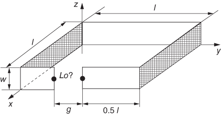
Figure 5.9 Example geometry for open-loop inductance computation.

Figure 5.10 Open-loop inductance example for geometry in Fig. 5.9.
5.5 Computation of Partial Inductances
It is evident that the PEEC method leads to an efficient approach for the computation of inductances for any structure. Unfortunately, the evaluation of the partial inductances is not straightforward. The computation of exact partial inductances can be time consuming, while some approximate formulas designed before computers were available [1] may not be accurate enough for closely spaced conductors. A recent text makes a valuable contribution to partial inductance computations [2].
The aim of our Appendix C is to provide a list of partial inductances that are convenient to use for the evaluation of partial inductances. The approach is to use analytic expressions wherever possible. However, this does not exclude the use of numerical integration where necessary. Especially for some nonorthogonal and other complex geometries, we have to apply numerical integration concepts where analytic formulas are hard to find. Fortunately, continuous progress is being made by many researchers, for example, Refs [3, 14–16].
Other important details must be observed to obtain efficient, accurate partial inductances. Hence, we focus on this issue since it is key for practical computation. The evaluation of the partial inductance ![]() (5.17) requires the integration over two volumes or six coordinates,
(5.17) requires the integration over two volumes or six coordinates, ![]() . Clearly, obtaining reasonable inductances without computers was at best tedious in the precomputer era [1]. Still, the exact partial inductance computations can be too time consuming since the speed of the evaluation of the partial inductances can limit the size of problems we can solve.
. Clearly, obtaining reasonable inductances without computers was at best tedious in the precomputer era [1]. Still, the exact partial inductance computations can be too time consuming since the speed of the evaluation of the partial inductances can limit the size of problems we can solve.
Many researchers aimed at reducing the compute time for each ![]() given by (5.17). A simple implementation requires
given by (5.17). A simple implementation requires ![]() partial inductances to be evaluated. However, due to the symmetry of the
partial inductances to be evaluated. However, due to the symmetry of the ![]() matrix, only
matrix, only ![]() partial inductances must be evaluated. A general approach for the efficient evaluation of partial inductances is the multifunction technique, which is a mixture of many different approaches considered in [15, 16] and Appendix E. A small example of the integration simplification is given in the following section. Today, other techniques can be applied to speed up the computation of partial inductance matrices. They basically take advantage of the reduced rank [17] of the
partial inductances must be evaluated. A general approach for the efficient evaluation of partial inductances is the multifunction technique, which is a mixture of many different approaches considered in [15, 16] and Appendix E. A small example of the integration simplification is given in the following section. Today, other techniques can be applied to speed up the computation of partial inductance matrices. They basically take advantage of the reduced rank [17] of the ![]() matrix [11]. However, we do not consider these techniques in this text.
matrix [11]. However, we do not consider these techniques in this text.
5.5.1 Approximate Formulas for Partial Inductances
As an example, volume filament (VFI) models for the skin effect considered in Chapter 9 need very accurate partial inductance evaluations due to the close spacing of the filament conductors. However, carefully applied approximate partial inductance formulas [1] and [2] are sufficient for some simple PEEC models. To make sure that they are applied appropriately, we labeled the approximate ![]() 's as such in Appendix C. Also, we need to consider numerical integration methods for different approximations. The high accuracy needed for some partial inductances may result in relatively large compute time if numerical techniques are used. Often, very good results can be obtained with sufficient accuracy if careful mixed analytic and numerical integration methods are used.
's as such in Appendix C. Also, we need to consider numerical integration methods for different approximations. The high accuracy needed for some partial inductances may result in relatively large compute time if numerical techniques are used. Often, very good results can be obtained with sufficient accuracy if careful mixed analytic and numerical integration methods are used.
Next, we give an example for an approximate partial mutual inductance formula for distant conductors. Consider the case where two relatively short conductors are widely spaced. It is clear that approximations can be used if the distance ![]() between too small conductors is large compared to the conductor size. We use the exact partial inductances as
between too small conductors is large compared to the conductor size. We use the exact partial inductances as

This formula works for both orthogonal and nonorthogonal coordinates. A convenient further approximation yields

where ![]() and
and ![]() are the length of filament approximation segments that are placed at the center of the cell cross sections. Here,
are the length of filament approximation segments that are placed at the center of the cell cross sections. Here, ![]() is the angle between the filaments.
is the angle between the filaments.
It is clear that this approximate formula can save compute time for distant conductors. In fact, the majority of couplings are far distance for large problems. In Section 5.7, we use (5.20) for the case of rectangular cross section, transmission line (TL) type, and ground plane geometry.
Other precomputer formulas for partial inductance have been given in Refs [18] and [1]. For example, the partial self- inductance of a rectangular bar is simplified to

where ![]() is the variable length and
is the variable length and ![]() is the width, and
is the width, and ![]() is the thickness of the rectangular bar.
is the thickness of the rectangular bar.
We compare the exact rectangular bar formula (C.35) from Appendix C with the result of the formula (5.22) in Fig. 5.11 using W = 1 mm and T = 0.2 mm as a function of the length. It is evident that such an error of several percent in the partial inductances can lead to poor overall inductance results.

Figure 5.11 Error in  for approximate formula.
5.5.2 Inductance Computations for Large Aspect Ratio Conductors
An important advantage of the PEEC method is that we often can make models with cells that are very long or wide in comparison to other dimensions. This is in part due to the special meshing that is employed by the approach as is presented in Chapter 8. This is in contrast to other methods such as the finite difference time domain (FDTD), finite integration (FIT), transmission line matrix (TLM), or finite element (FEM) and other integral equation (IE) methods where the ratio between the sides of a cell is limited. In fact, a desired ratio of length to width close to one is not unusual. PEEC cells of large aspect ratio are desirable for the type of problem we want to solve since a large gain in efficiency is possible for some geometries.
We should note that the evaluation of the partial inductances is difficult for extreme geometries. For this reason, we want to understand the limit of the side aspect ratios for which the partial inductance computation may become inaccurate. It should be clear that each analytic formula or inductance shape has its own limit. Other researchers have also considered this issue [14]. An extreme ratio for the dimensions may be a ratio of 10,000:1 for the length to width or thickness of a conductor. The limiting factor is that some of the analytic formulas for a partial self- or mutual inductance are very elaborate. It is this complexity that leads to numerical errors even if we use double precision arithmetic in the evaluation.
Several papers assert that the PEEC approach is not suitable for very long, narrow, parallel line-type structures and that the computation of loop inductance should be used to solve this problem. We show that, in fact, this is not the case. However, correctly solving the aspect ratio problem is not trivial. The proper solution of this problem involves two aspects. One aspect that relates to the PEEC model is considered in this section, whereas the second issue that relates to the evaluation of the partial inductances is considered in the following section.
Not surprisingly, it is difficult to evaluate partial inductance with a high accuracy for extreme geometries. As an example geometry, it is sufficient to consider a typical loop shown in Fig. 5.4. Here, we consider a physically long version shown in Fig. 5.12. The circuit solution for the loop inductance is given in (5.16). We regroup the terms of the equation in pairs in the form
It is apparent from Fig. 5.12 that we assume that the length ![]() of the loop is large compared to the spacing
of the loop is large compared to the spacing ![]() . The length consists of the partial self inductances
. The length consists of the partial self inductances ![]() and
and ![]() , while the orthogonal end branches have the partial self-inductances
, while the orthogonal end branches have the partial self-inductances ![]() and
and ![]() . Note that due to the orthogonality of the conductors, the only nonzero partial mutual inductances are
. Note that due to the orthogonality of the conductors, the only nonzero partial mutual inductances are ![]() and
and ![]() .
.

Figure 5.12 Long loop represented by four bars.
Now, we want to consider the case where the two bars with ![]() and
and ![]() are very long, or
are very long, or ![]() . Approximations can be used for the end branch inductances since they are very short compared to the long branches of length
. Approximations can be used for the end branch inductances since they are very short compared to the long branches of length ![]() . Clearly, the partial mutual inductances
. Clearly, the partial mutual inductances ![]() and
and ![]() will become very small due to the large coupling distance that is approximately
will become very small due to the large coupling distance that is approximately ![]() and the lengths are
and the lengths are ![]() . In fact, we can approximate
. In fact, we can approximate ![]() using (5.21).
using (5.21).
Further, the end partial self-inductances are small. Hence, we can either ignore them or just add the partial end self-inductances that are ![]() and
and ![]() to the loop inductance. Of course, for very large lengths, their contributions can also be approximated to be zero without impacting the results we want to show.
to the loop inductance. Of course, for very large lengths, their contributions can also be approximated to be zero without impacting the results we want to show.
The key problem is the treatment of partial inductances where the length ![]() is much larger than all other conductor dimensions. Also, a very interesting limiting case is given by
is much larger than all other conductor dimensions. Also, a very interesting limiting case is given by ![]() . Another important observation is that such conductors must be close to each other like a TL, else the inductance reaches such large values that this would not represent a reasonable physical situation. In the loop example, this implies that
. Another important observation is that such conductors must be close to each other like a TL, else the inductance reaches such large values that this would not represent a reasonable physical situation. In the loop example, this implies that ![]() is small. If we ignore the small end inductances, the loop inductance (5.23) simplifies to
is small. If we ignore the small end inductances, the loop inductance (5.23) simplifies to
Taking the partial self-inductance alone, we get ![]() . Hence, it would be a mistake to independently evaluate each partial inductance in (5.24). Instead, for long complex geometries, we take pairs of partial inductances such that each partial self-inductance has a closing part. Then, we define each pair a difference inductance where
. Hence, it would be a mistake to independently evaluate each partial inductance in (5.24). Instead, for long complex geometries, we take pairs of partial inductances such that each partial self-inductance has a closing part. Then, we define each pair a difference inductance where ![]() and
and ![]() . Then the approximate inductance for the loop with very long conductors 1 and 3 given by
. Then the approximate inductance for the loop with very long conductors 1 and 3 given by ![]() . We consider the careful computation of the difference inductances and the partial inductances in the following section. The important observation is that per unit length difference inductances are given by
. We consider the careful computation of the difference inductances and the partial inductances in the following section. The important observation is that per unit length difference inductances are given by
where ![]() is a constant finite asymptotic value. This behavior strongly depends on the formulas used for the partial inductance. This aspect is considered in the following section.
is a constant finite asymptotic value. This behavior strongly depends on the formulas used for the partial inductance. This aspect is considered in the following section.
The difficulties in the evaluation of partial inductance for extreme aspect ratios of the conductors were known from the start of computer- based solutions [3]. It was found that the evaluation of complex formulas for the partial inductances may lead to very unreliable results for extreme dimensions [14, 19]. The essence of the problem can be reduced to two closely located very long conductors with equal and opposite currents that we assume to be of the same size.
It is clear from (5.24) that the difference inductances converge according to (5.25) if both partial inductance formulas in ![]() have the same asymptotic behavior. This means that the partial mutual inductance formulation for
have the same asymptotic behavior. This means that the partial mutual inductance formulation for ![]() must, in the limit, give exactly the same result as the partial self-inductances
must, in the limit, give exactly the same result as the partial self-inductances ![]() . Practically, five digits of accuracy in the partial inductances is sufficient for extreme geometries.
. Practically, five digits of accuracy in the partial inductances is sufficient for extreme geometries.
Next, we want to consider the evaluation of the difference inductances for a realistic example. Important is the asymptotic behavior with respect to a long length ![]() . In the first example, a loop of round conductors with a radius
. In the first example, a loop of round conductors with a radius ![]() is used. We need to emphasize that these formulas found in Refs [1, 2] are approximations [20].
is used. We need to emphasize that these formulas found in Refs [1, 2] are approximations [20].
The key reasons that we use these approximate formulas are they can be used for both the partial self- and mutual and that they have the same asymptotic behavior. However, this does not give any indication about the exactness of the result. Using this, the difference between the partial self- and mutual inductances can be written as

For very long lengths where ![]() , the partial inductances can be approximated as
, the partial inductances can be approximated as


Hence, for the case where both conductors have the same radius ![]() and the same length
and the same length ![]() , the approximate loop inductance is
, the approximate loop inductance is

Finally, again under the condition that ![]() , the per-unit length inductance is approximated as
, the per-unit length inductance is approximated as

We note that this corresponds to the usual approximate per-unit length inductance of a two round conductor TL for dimensions ![]() , which can be found in textbooks [21]. This derivation clearly shows partial and subinductance approaches can effectively be used to compute the inductance of long loops. Importantly, the same approach also works for multiple-loop situations.
, which can be found in textbooks [21]. This derivation clearly shows partial and subinductance approaches can effectively be used to compute the inductance of long loops. Importantly, the same approach also works for multiple-loop situations.
We next consider the same loop where the conductors consist of zero thickness sheets. The exact partial self- and mutual inductances are computed with the formula (C.24). We use the equation (C.19) for both the partial self- and the partial mutual inductances with the same asymptotic behavior for ![]() as for
as for ![]() . The zero thickness loop problem using formula (5.24) for two conductors of the same width also yields the same difference inductance
. The zero thickness loop problem using formula (5.24) for two conductors of the same width also yields the same difference inductance ![]() , where
, where ![]() .
.
Results are presented for the long loop example with the three different cross sections corresponding to Fig. 5.12, where the short return conductors are ignored. The cross section of the round conductors is ![]() . The zero thickness conductors have a width
. The zero thickness conductors have a width ![]() . Finally, the thickness for the rectangular conductors is
. Finally, the thickness for the rectangular conductors is ![]() and the length for all conductors is increased over a wide range from
and the length for all conductors is increased over a wide range from ![]() to
to ![]() . Hence, the smallest to largest dimension is 1 : 3000. We have the zero and finite thickness conductors touching each other on the width side as would be the case for a VFI skin-effect model. For this case,
. Hence, the smallest to largest dimension is 1 : 3000. We have the zero and finite thickness conductors touching each other on the width side as would be the case for a VFI skin-effect model. For this case, ![]() will be only slightly larger than
will be only slightly larger than ![]() . Hence, this is the most critical case to consider for the accuracy issue.
. Hence, this is the most critical case to consider for the accuracy issue.
Figure 5.13 shows a comparison for the partial self- inductance divided by the length for the three different cases using the approximate round wire formula (5.27) “(Round),” the zero thickness formula (C.19) “(Zero),” and also the exact volume formula for an equivalent area square shape given in Appendix C (C.35) as “(Finite).”

Figure 5.13 Partial self-inductance divided by length for different cross sections.
Similarly, in Fig. 5.14 partial mutual inductance formulas are compared where we see inaccuracies for large lengths for the “(Finite)” result in Appendix C for two rectangular bars.

Figure 5.14 Partial mutual inductance divided by length for different cross sections.
Figure 5.15 shows the subtraction of the self and the mutual ![]() . This subtraction takes place in most formulas. For lengths larger than 2 m, inaccuracies appear in the rectangular formulas using double precision due to their increased complexity. Hence, for this case, other practical techniques such as breaking up the length of the conductor into segments are used.
. This subtraction takes place in most formulas. For lengths larger than 2 m, inaccuracies appear in the rectangular formulas using double precision due to their increased complexity. Hence, for this case, other practical techniques such as breaking up the length of the conductor into segments are used.

Figure 5.15 Subinductances divided by length for different cross sections.
This comparison shows that even for large aspect ratios, the simpler partial inductance formulas give consistent results. However, for the finite thickness conductor loop, the difference inductance becomes very inaccurate for long length. This is due to the more complicated analytic formulas for the partial inductances. This example illustrates how very complex formulas for the partial inductances can lead to inaccuracies in the inductance evaluation. We should mention that the example of extreme aspect ratios for the dimensions does not only apply to conductor length, but cells or conductors with other extreme dimension ratios can also lead to similar problems.
One of the advantages of the partial inductance concept is the ability to break a complicated three-dimensional problem into its constituent interactions resulting for general inductance calculations. In this section, we use a small PEEC model to address the accuracy issue that is encountered in dense problems. This is done using the two- conductor example from Fig. 5.12. In this approximate model, we represent each conductor by a partial inductance. If we ignore the vertical connections at the two ends, its inductance is approximated as ![]() .
.
The inherent source of errors is due to the subtraction of the partial inductances for the closely located conductors. For close neighbor conductors, the first two digits in the partial inductances may be the same for ![]() and
and ![]() and only the third digit may contain information relevant for the result. Hence, a key source of problems is the exact computation of the partial inductances. Many formulas are not robust at all, especially for large conductor aspect ratios. Robust
and only the third digit may contain information relevant for the result. Hence, a key source of problems is the exact computation of the partial inductances. Many formulas are not robust at all, especially for large conductor aspect ratios. Robust ![]() computations for large aspect ratios are mandatory for PEEC.
computations for large aspect ratios are mandatory for PEEC.
We should use the formulas in Appendix C that are labeled exact. As we exemplified in the previous section, exact analytic formulas can also lead to errors even using double precision arithmetic for the computations. For this reason, we sometimes resort to the mixed analytic and numerical calculations. The analytic and the numerical evaluation of the integrals can be complementary. The weakness of analytic formulas can be very long conductors as we illustrated. However, the numerical integration along the long direction is also a poor idea due to the long compute times.
To give an example of the analytic-numerical evaluation, we use long filament partial inductances ![]() for a very long small cross-sectional wire. For filaments, we can apply the partial inductance formula for long conductors due to the simplicity of the formula (C.2). In this case, the filament
for a very long small cross-sectional wire. For filaments, we can apply the partial inductance formula for long conductors due to the simplicity of the formula (C.2). In this case, the filament ![]() carries the entire subsection current. To compute the partial inductance for a conductor with an arbitrary cross section, we use
carries the entire subsection current. To compute the partial inductance for a conductor with an arbitrary cross section, we use

A variety of approximations for the cross-sectional integrals can be used. For small cross sections, the evaluation of the integrals over the cross sections ![]() and
and ![]() can efficiently be evaluated numerically using Gaussian integration, which is presented in Appendix E.1.1.
can efficiently be evaluated numerically using Gaussian integration, which is presented in Appendix E.1.1.

Figure 5.16 Open-loop inductance for three bars in series.
5.6 General Inductance Computations Using Partial Inductances and Open Loop Inductance
It should be apparent at this point that partial inductances provide a flexible approach for the computation of the inductance for arbitrary geometries. In this section, we give simple examples to illustrate the use of some of the concepts given earlier.
The simple example includes three metal strip cells in series as shown in Fig. 5.16. Since they clearly do not form a loop, we can only compute the open-loop inductance ![]() for the three metal bars connected to each other.
for the three metal bars connected to each other.
The partial inductance matrix for this problem is given in (5.32), where all the partial inductances are computed as reported in the previous section.

We recognize that all the currents in the bars are same. Hence, we have
and the total voltage along all three bars is
Finally, to compute the open-loop inductance, ![]() . We recognize that the result is obtained by adding all the partial inductances in the matrix in (5.32). We assume that all three conductors have the same length
. We recognize that the result is obtained by adding all the partial inductances in the matrix in (5.32). We assume that all three conductors have the same length ![]() . For this case, solving the above equations can be reduced to the open loop inductance
. For this case, solving the above equations can be reduced to the open loop inductance
Of course, the symmetry of the ![]() matrix is used to simplify the result.
matrix is used to simplify the result.
5.6.1 Closing the Loop for Open-Loop Problems
We next set up a closed-loop example based on the open-loop example considered in the previous section. Figure 5.16 gives the example in Fig. 5.17 with a possible closing loop. We notice that the two sides are orthogonal to the horizontal cells. Hence, the only couplings between the sides are ![]() and
and ![]() . However,
. However, ![]() is coupled to the three horizontal cells. Again, the current in all the cells is same,
is coupled to the three horizontal cells. Again, the current in all the cells is same, ![]() .
.

Figure 5.17 Loop inductance for three bars in series.
As reported in Section 5.4.2, we use the open-loop inductance ![]() for three lower bars (5.35) as part of solution. The three lower conductor cells have the same size. This is also true for the two side conductors. We can set up the partial inductance matrix for the larger problem. However, the result can also be constructed by inspection as
for three lower bars (5.35) as part of solution. The three lower conductor cells have the same size. This is also true for the two side conductors. We can set up the partial inductance matrix for the larger problem. However, the result can also be constructed by inspection as
where the expression takes advantage of the symmetry of the ![]() matrix and
matrix and ![]() .
.
A general observation is that in many models, partial or incomplete inductances are not marked as such. Errors may result since we know that open-loop inductances in Fig. 5.16, without a closing path like the one shown in Fig. 5.17, represent an incomplete macromodel.
It is important for us to deal with this situation since too many models, with incomplete open loops, lead to wrong results.
5.7 Difference Cell Pair Inductance Models
In Section 5.5.2, we observed the behavior of the difference inductance between
where ![]() is again the parallel conductor length. This yields finite results for long structures where
is again the parallel conductor length. This yields finite results for long structures where ![]() is in contrast to the partial self-inductance; where as the length
is in contrast to the partial self-inductance; where as the length ![]() goes to
goes to ![]() , we have
, we have
An interesting set of difference models are based on symmetrical conductor TL-type models with conventional voltage difference ports with equal and opposing currents. For these structures, the difference inductance is finite. This is considered in the following section.
5.7.1 Inductances for Transmission Line-Type Geometries
We consider the inductance for TL-type inductance models [22, 23] in this section. We consider finite models for TL-type structures that cannot be obtained with conventional transverse electromagnetic (TEM) models. The models usually consist of long uniform cross-sectional structures. To generalize the models, we could also apply the VFI skin-effect models in Section 9.3 to all the conductors in the models. However, in this section we do not consider skin-effect issues. TEM TL conductors are theoretically infinite in length. Here we investigate real-life finite length lines and limit the models to inductances only. However, capacitance models that are not considered can be modeled similarly.
An interesting observation is that the conventional TL model is based on a differential equation representation. Still, it is important to understand that the per-unit length TEM-TL cross-sectional capacitances and inductances are usually computed with a 2D IE solver. The difference between the 2D TL models is the finite length of the 3D PEEC models that are considered in this section.
Partial inductances for wires that are long compared to the cross section are considered in Section 5.5.2. This is very useful for some very long wire model. By now it is clear that PEEC section models are based on coupling between all cells in the model. This is much different from the conventional TEM-TL models where the inductances models are not coupled along the length. These 1-D type models are based on the assumption that the line is infinitely long with a uniform cross-section.
Clearly for real-life TLs, practical errors result if the finite conductor length is relatively short compared to the cross-sectional conductor to ground spacing. For conventional TL models to give a reasonably accurate answer, a realistic length ![]() to wire-to-wire cross-sectional spacing
to wire-to-wire cross-sectional spacing ![]() , ratio
, ratio ![]() should be larger than 10–20.
should be larger than 10–20.
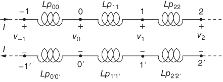
Figure 5.18 Finite two-wire line represented in terms of partial inductances.
Fortunately, for finite length TL structures we can use partial inductance-based models to eliminate the length error. A PEEC model based on partial inductances that represents a section of a TL model is shown in Fig. 5.18. For this model, we chose the range for the section number to be from ![]() to a positive
to a positive ![]() , so that the line can be extended to
, so that the line can be extended to ![]() in both directions. For a semi-infinite line, we can cut the model anywhere, for instance with
in both directions. For a semi-infinite line, we can cut the model anywhere, for instance with ![]() .
.
Compute the inductance for a single section k in Fig. 5.18. The voltage drop along the section is

which is the voltage induced in the ![]() th section in (5.39) including all the partial mutuals. We note that if our model extends from
th section in (5.39) including all the partial mutuals. We note that if our model extends from ![]() to
to ![]() , then the section inductance is the same as that of a conventional TEM-TL model. The inductance for section
, then the section inductance is the same as that of a conventional TEM-TL model. The inductance for section ![]() in (5.39) can be rewritten in a more simple form as
in (5.39) can be rewritten in a more simple form as

for an infinitely long line. If both conductors have the same cross sections for the symmetric situation where ![]() , then we can apply what we call a difference inductance as
, then we can apply what we call a difference inductance as
to simplify the (5.40).
The concept of difference inductances is also efficient for other applications such as multiple TLs or other double-layer plane inductances as is considered in the following section. Of course, the cell pairs must be located directly above each other with opposing currents. The general case for coupling ![]() between two cell pairs
between two cell pairs ![]() and
and ![]() is shown in Fig. 5.19. The coupling inductance can be computed as
is shown in Fig. 5.19. The coupling inductance can be computed as
with the difference inductance given in (5.41).

Figure 5.19 Coupling pairs for two plane conductor cell pair.
5.7.2 Approximate Inductive Coupling Calculation Between Difference Cell Pairs
The evaluation of all the partial or difference inductances can be very time consuming. We consider simplification and speedup of the evaluation of partial inductances for the dense sections of the MNA circuit matrix. First, we observed that the coupling from section to section decays much faster than the ![]() behavior of the conventional partial inductances where
behavior of the conventional partial inductances where ![]() is the center-to-center distance between the conductor cell pairs shown in Fig. 5.19. Hence, the difference inductance-based matrices can be sparsified, while this is not the case for matrices of conventional sparse matrices.
is the center-to-center distance between the conductor cell pairs shown in Fig. 5.19. Hence, the difference inductance-based matrices can be sparsified, while this is not the case for matrices of conventional sparse matrices.
We want to apply the simplification of the ![]() matrices for the general case shown in Fig. 5.19.
matrices for the general case shown in Fig. 5.19.
The geometry illustrated does not only consider the single TL inductance case where both cell pairs are along the ![]() -axis but also the more general case for plane pairs that is treated in Section 5.7.4. The evaluation of the exact formulas for
-axis but also the more general case for plane pairs that is treated in Section 5.7.4. The evaluation of the exact formulas for ![]() is based on using conventional partial inductance formulas given in Appendix C. The basic inductance formulation for the two coupled cell pairs is given in (5.41).
is based on using conventional partial inductance formulas given in Appendix C. The basic inductance formulation for the two coupled cell pairs is given in (5.41).
A second, fast approximate evaluation of (5.41) is based on the filament approximation given in (5.21) for the partial inductance, or

where ![]() and
and ![]() are the cell lengths parallel in the
are the cell lengths parallel in the ![]() -direction. Further, the cell center-to-center distance between the cell pairs is
-direction. Further, the cell center-to-center distance between the cell pairs is
where we assume that ![]() is the same vertical cell distance for both pairs and that all cells are in the same planes such that
is the same vertical cell distance for both pairs and that all cells are in the same planes such that ![]() . For the TL case, we have
. For the TL case, we have ![]() and for the cells at the same level or
and for the cells at the same level or ![]() .
.
We can rewrite the distance metric for the ![]() to
to ![]() case as
case as

This leads to the approximate partial inductance using (5.21) for distant conductors that couples between the planes at the two different levels

where in the last step we approximate the square root with a series expansion under the condition that ![]() . This leads to the approximate section-to-section coupling
. This leads to the approximate section-to-section coupling

where the center-to-center distance ![]() in Fig. 5.19 is large compared to the plane-to-plane distance
in Fig. 5.19 is large compared to the plane-to-plane distance ![]() .
.
We give an example for the reduction of the error with cell distance in the approximate section-to-section inductance ![]() . In this example, the cells are square with
. In this example, the cells are square with ![]() 1 mm since square cells are representing a worst case, which is also important for the plane-pair models in the following section. In this example, the vertical cell spacing is 0.2 mm. The fast in-plane spacing decay is evident from Table 5.1. The error is the normalized difference between the exact and approximated formula (5.47). We observe that this is the worst case in comparison to narrower cells. Also, results are given in Table 5.1, where each cell is represented by a two- wire Gaussian integration approximation, with a reduction in error of about a factor 2 for sufficient spacing. This leads to an even faster decay of the coupling.
1 mm since square cells are representing a worst case, which is also important for the plane-pair models in the following section. In this example, the vertical cell spacing is 0.2 mm. The fast in-plane spacing decay is evident from Table 5.1. The error is the normalized difference between the exact and approximated formula (5.47). We observe that this is the worst case in comparison to narrower cells. Also, results are given in Table 5.1, where each cell is represented by a two- wire Gaussian integration approximation, with a reduction in error of about a factor 2 for sufficient spacing. This leads to an even faster decay of the coupling.
Table 5.1 Comparison of section-to-section coupling inductance decay.
| Section Distance (mm) | 1 Fil. appr. |
Error ( |
2 Fil. appr. |
Error | |
| 1 | 21.978 | 4.00 | 81.80 | 5.0095 | 77.21 |
| 2 | 0.62408 | 0.5000 | 19.88 | 0.54407 | 12.82 |
| 3 | 0.16161 | 0.14815 | 8.33 | 0.15418 | 4.60 |
| 5 | 0.032963 | 0.03200 | 2.92 | 0.032477 | 1.47 |
| 8 | 0.0079019 | 0.0078125 | 1.31 | 0.0078582 | 0.55 |
| 10 | 0.0040291 | 0.0040000 | 0.72 | 0.0040150 | 0.35 |
| 15 | 0.00118980 | 0.00111852 | 0.32 | 0.0011872 | 0.15 |
5.7.3 Inductance of Finite and Semi-Infinite Length TL
The coupling computations in the previous paragraph seem to work also for the coupling between length sections of a TL. The fundamental coupling equation used (5.21) gives the partial inductance conductors for two distant filaments. Now, the equation derived in the previous section (5.47) ![]() gives the coupling for conducting pairs with opposite currents as is the case in TLs, which is based on the difference inductances.
gives the coupling for conducting pairs with opposite currents as is the case in TLs, which is based on the difference inductances.
We apply the difference coupling equations to the TL formulation in Section 5.7.1 to study the coupling between TL sections. Very often, we do not take the coupling between length sections into account. For this reason, we study impact of the lack of length inductive coupling between the segments. We cut the TLs into ![]() independent sections as shown in Fig. 5.19. In the comparison, we construct two models, one with couplings between all sections and one where the couplings between the sections are ignored. The error between the two solutions with and without couplings is computed. In summary, the section coupling between sections 1 and 2 is evaluated according to (5.40) as
independent sections as shown in Fig. 5.19. In the comparison, we construct two models, one with couplings between all sections and one where the couplings between the sections are ignored. The error between the two solutions with and without couplings is computed. In summary, the section coupling between sections 1 and 2 is evaluated according to (5.40) as
where the approximate formula (5.47) is used, while the case of all coupled ![]() sections is the same as the difference inductance for the entire two-wire line.
sections is the same as the difference inductance for the entire two-wire line.
In Table 5.2, ![]() represents the inductance of the calculation of the wires with all couplings. Again, the section model in Fig. 5.20 consists of
represents the inductance of the calculation of the wires with all couplings. Again, the section model in Fig. 5.20 consists of ![]() uncoupled parts.
uncoupled parts.
Table 5.2 Comparison of TL inductance v.s. the number of sections.
| Sections |
||
| 1 | 0.27765 | 0.27765 |
| 2 | 0.582049 | 0.555299 |
| 4 | 1.196842 | 1.110598 |
| 6 | 1.813189 | 1.665898 |
| 8 | 2.429942 | 2.221197 |
| 10 | 3.046943 | 2.776496 |

Figure 5.20 Transmission line model with line sections and equivalent circuit.
It is not surprising that the error increases as the number of noncoupled ports increases.
5.7.4 Plane Pair PEEC Models Based on Difference Currents
In the previous section, we showed that the inductive coupling between distant cell pairs drops off fast due to the canceling effect of the opposing currents in the partial inductance pairs. The same concepts lead to interesting application to the modeling for power plane pairs [24–26]. The purpose of the so-called power distribution network (PDN) is to supply voltage and ground to the integrated circuits (ICs).
We apply the current difference approach defined in Section 5.5.2 to plane pairs for printed circuit board [27, 28]. The approach also benefits from the rapid coupling decay that leads to a sparse circuit matrix. We need to mesh the planes according to Chapter 8 by laying out the surfaces with congruent conventional mesh cells. Hence, the cell structure and the node current structure are the same on both surfaces similar to the TL model in Fig. 5.18. The equal and opposing currents in the plane cells as well as the voltage differences at congruent nodes at the same ![]() location lead to half the unknowns.
location lead to half the unknowns.
To keep the model simple, we consider a strictly inductance model. For the inductance-only model, the solution is fast since all the matrices are real. More complex parallel plane partial element equivalent circuit (PPP) models can include capacitances as well as resistances.
5.7.5 Parallel Plane PEEC Modeling
Realistic PC plane problems have specific connection and structures. The purpose of the decoupling capacitor used is to prevent the supply voltages from dropping due to the inductance of the path. The source of the voltage drop is the switching integrated circuits. The objective of the technique presented in this section is the efficient evaluation of the inductance between a pair of power planes that is part of the PDN circuit. The most simple example of such a plane pair distribution system is shown in Fig. 5.21.

Figure 5.21 Parallel power planes example with IC and decoupling capacitor.
The power plane system supplies the voltages to the appropriate pins at an IC. Usually, large decoupling capacitors keep the impedance (inductance) as low as possible between the supplied voltage and ground. An assumption made is that the frequency is high enough such that the skin depth (9.1) compared to the thickness of the conductors is small and all current flows between the inner surfaces of the plane pair shown in Fig. 5.21. Hence, the thickness of the planes isolates the currents to the inside the planes.
More generally, PPP cases are considered in Ref. [29] for both frequency and the time domain solutions. In this section, we are interested in inductance computation only under the condition that the impedance of the large decoupling capacitor(s) is inductive. Such a plane pair in general has multiple connections that can be capacitors, voltage, and ground via connections. Via connections are inductive at mid frequencies.
The approximate inductance for a decoupling capacitor is called ESL which is usually specified by the manufacturer. In fact, we consider the inductance modeling of a capacitor in Section 5.4.1. Fortunately, we can use a simple partial inductance model for the via connections, similar to the pin partial inductance in Fig. 5.8. Due to the orthogonality, the partial mutual inductances between the planes and vias are zero or very small. Hence, we can separate the plane inductances from the via inductances.
5.7.6 PEEC Inductance Plane Model with Orthogonal Meshing
We use them to represent the plane inductance in this model. We use the most simple example to explain the PPP formulation for the parallel plane model. The example shown in Fig. 5.22 does include a current source for the IC shown in Fig. 5.21 and a short circuit between the planes that represents a perfect decoupling capacitor. To keep the example simple, a minimum number of circuit elements are used. Each plane is represented by only four partial inductances shown in Fig. 5.22. We make the connection to the IC at node ![]() with the current source. The decoupling capacitor is located at node
with the current source. The decoupling capacitor is located at node ![]() represented by a simple short circuit. Of course, the node pairs at each node represent ports between the plane pairs. For more realistic plane models, multiple capacitors ICs can be connected at available ports. At this point, we also assume that the difference inductances have been computed as reported in Section 5.7.2. We use them for inductances in this model.
represented by a simple short circuit. Of course, the node pairs at each node represent ports between the plane pairs. For more realistic plane models, multiple capacitors ICs can be connected at available ports. At this point, we also assume that the difference inductances have been computed as reported in Section 5.7.2. We use them for inductances in this model.

Figure 5.22 Small example geometry for two parallel plane PEEC model.
We set up the MNA equations for the simple test geometry in Fig. 5.22 according to Chapter 2. Here, the equations include voltage differences at the nodes and the opposing difference currents are between the planes leading to difference inductances ![]() as given by (5.41). The reduction of unknowns is clear from this. The fundamental aspects of the MNA matrix are very similar, and we can use the circuit elements stamps in Appendix B. The MNA equations for the difference quantities is given by
as given by (5.41). The reduction of unknowns is clear from this. The fundamental aspects of the MNA matrix are very similar, and we can use the circuit elements stamps in Appendix B. The MNA equations for the difference quantities is given by

At the node port ![]() , we can compute the port inductance as
, we can compute the port inductance as ![]() . For example, we inject a unit current of
. For example, we inject a unit current of ![]() and we measure the voltage leading to the inductive impedance in k
and we measure the voltage leading to the inductive impedance in k![]() . The system would lead to a complex solution if we include the plane resistance in the model.
. The system would lead to a complex solution if we include the plane resistance in the model.
The basic ordering of the equations is given in (5.49). To make it clear, we also show the matrix structure in Fig. 5.23. The entries corresponding to the Kirchhoff's current law (KCL) ![]() matrix parts are set up automatically by the inductance stamps. They can also be set up using matrix KCL stamps as is done in Section 2.7.1. We observe that the difference inductance
matrix parts are set up automatically by the inductance stamps. They can also be set up using matrix KCL stamps as is done in Section 2.7.1. We observe that the difference inductance ![]() part is represented in decoupled
part is represented in decoupled ![]() and
and ![]() parts avoiding
parts avoiding ![]() couplings. Further, adding the equations for short circuits is done at the last rows and columns. This facilitates changes such as adding other elements, for example, the addition of more decoupling capacitors to the solution. As is shown, the computationally expensive inductance part of the PEEC model and part of the MNA matrix are not impacted by adding elements to the model. The matrix equation ordering leads to flexibility in changes of the circuit topology.
couplings. Further, adding the equations for short circuits is done at the last rows and columns. This facilitates changes such as adding other elements, for example, the addition of more decoupling capacitors to the solution. As is shown, the computationally expensive inductance part of the PEEC model and part of the MNA matrix are not impacted by adding elements to the model. The matrix equation ordering leads to flexibility in changes of the circuit topology.

Figure 5.23 General schematic MNA matrix with additional equations.
5.7.7 Mesh Reduction Without Couplings of Nonparallel Inductances
So far, the formulation presented here avoids the coupling between the orthogonal matrix parts. We presented in this section how this is accomplished even for a mesh-size reduction. Several levels of mesh reduction are used to speed up the solution. Smaller mesh sizes near the contacts increase the accuracy of the solution. Also, the mesh size is increased for open areas to reduce the compute time. The advantage of a variable mesh size for the compute time can be considerable as is shown in Ref. [29]. Conventionally, the change in mesh size requires nonorthogonal cells. However, this results in the undesirable coupling between the ![]() and
and ![]() submatrices in the MNA matrix in Fig. 5.23. The approximate decoupled model in Fig. 5.24 shows nodes corresponding to larger cells and the refined mesh to half the cell size. The connection between smaller cells and larger cells must be established. We accomplish this with a so-called weighted KCL approach, which is presented next.
submatrices in the MNA matrix in Fig. 5.23. The approximate decoupled model in Fig. 5.24 shows nodes corresponding to larger cells and the refined mesh to half the cell size. The connection between smaller cells and larger cells must be established. We accomplish this with a so-called weighted KCL approach, which is presented next.

Figure 5.24 Mesh at corner interface between coarse and fine mesh.
The PEEC inductance model corresponding to the meshing in Fig. 5.24 is shown in Fig. 5.25. We see from both figures that only half the refined mesh cells are connected directly at the boundary. Hence, a discontinuity results between the two regions. To take care of this situation, we locally modify the KCL equations.
Figure 5.25 Equivalent circuit for reduction of meshing example for PPP inductance model.
Fundamentally, we redirect some of the current to the unconnected nodes of the fine mesh. We observe that we set up different weighted KCL equation near the corners depending on the location of the local nodes. Different weights have to be used for a convex and a concave corner as shown in Fig. 5.24. The weights are chosen such that the current distributed is as close as possible to the one without the mesh size reduction. Note that a factor 2 in mesh size is obtained at the interface as is evident from Fig. 5.24.
The nodes at the concave corner are considered first. As usual, we write the equation for currents leaving the nodes. The KCL for the corner node ![]() is
is
The KCL for the node ![]() next to the concave corner is
next to the concave corner is
At the node ![]() , the approximate KCL for the noncorner node is
, the approximate KCL for the noncorner node is
The last two equations are used for all appropriate noncorner nodes.
The concave corner equations are similar with understandably somewhat different weighting factors. The KCL equation at the corner ![]() is given by
is given by
Finally, the KCL for neighbor node ![]() next to the convex corner is
next to the convex corner is
These weighted KCL equations cover all possible node configurations at the interface. The weights were found by comparing local currents with and without the interface such that it results in a good approximation of the local current density.
The mesh increase and reduction has a large impact on compute time and accuracy. This has been shown in Ref. [29]. The test problem consists of a simple ![]() parallel plane configuration with a spacing of
parallel plane configuration with a spacing of ![]() . A symmetric source and short situation is used for this simple example with the source and the short
. A symmetric source and short situation is used for this simple example with the source and the short ![]() from each side. The source and short are placed in the middle
from each side. The source and short are placed in the middle ![]() from each side. Hence, the short to source spacing is
from each side. Hence, the short to source spacing is ![]() .
.
The results of the experiment are given in Table 5.3. It is evident that the reduction in compute time due to the submeshing is excellent for the experimental Matlab program used.
Table 5.3 Some results for the PPP method for ![]() cm planes.
cm planes.
| Solution details | Number of unknowns | Inductance (pH) | Comp. time (s) |
| CST | Not available | 345.7 | Not available |
| Uniform mesh | 77,404 | 349.3 | 172.0 |
| 1 Level submesh | 20,108 | 355.7 | 13.6 |
| 2 Level submesh | 6,836 | 357.5 | 2.5 |
| 3 Level submesh | 3,852 | 358.5 | 1.5 |
5.8 Partial Inductances with Frequency Domain Retardation
The evaluation of partial elements with retardation is an important issue for high frequencies where the quasistatic solutions are inadequate. Delay or retardation from a circuit point of view is addressed in Section 2.11.1. Retardation for full-wave (FW) solutions is considered in Chapter 3. Furthermore, full-wave (FW)PEEC models are developed in Chapter 6. In this section, we consider the retardation issue from a partial inductance perspective. The retarded potential coefficient issues are quite similar, but they are not considered.
As an intermediate solution between the quasistatic and the high- frequency solution, it may be sufficient to include the retardation from cell center to cell center. The maximum cell size of ![]() may limit the error to be sufficiently small if the
may limit the error to be sufficiently small if the ![]() is small or if the conductors are small in size, unlike the example shown in Fig. 5.26.
is small or if the conductors are small in size, unlike the example shown in Fig. 5.26.

Figure 5.26 Two-bar example for a retarded partial inductance computation.
In the time domain, we mostly utilize the center-to-center delay. For the two conductors example in Fig. 5.26, we may have to further subdivide the conductors such that the cell size is small enough. The retardation time ![]() in the time domain is simply a delay between two points in space
in the time domain is simply a delay between two points in space ![]() and
and ![]() as given in (2.11.1) as
as given in (2.11.1) as
where ![]() is the velocity in the material and where in Fig. 5.26
is the velocity in the material and where in Fig. 5.26
In air ![]() , the speed of light, and in a lossless dielectric it is
, the speed of light, and in a lossless dielectric it is ![]() , where
, where ![]() is the relative dielectric constant. The time domain solver will have to take the delay of the couplings into account, a feature that is missing in a conventional SPICE circuit solver in both the time and the frequency domains.
is the relative dielectric constant. The time domain solver will have to take the delay of the couplings into account, a feature that is missing in a conventional SPICE circuit solver in both the time and the frequency domains.
For FW frequency domain solutions, the accuracy is improved if we also take the retardation inside the integral into account. The retardation is distributed over the areas of the cells. This leads to the following integrals for partial inductances. The formulation including the retardation term according to Section 3.4.2 is given by

where ![]() and
and ![]() . To simplify, we call
. To simplify, we call ![]() .
.
We first consider the situation for the partial self-inductance with delay, which is ![]() . In this case, both integrations will be over the same body. Again, the maximum physical dimensions of the conductor is limited to
. In this case, both integrations will be over the same body. Again, the maximum physical dimensions of the conductor is limited to ![]() . This can be utilized to evaluate the delay term
. This can be utilized to evaluate the delay term
where ![]() . For the partial self-inductance, the exponent remains relatively small even for the highest angular frequency
. For the partial self-inductance, the exponent remains relatively small even for the highest angular frequency ![]() . For this reason, we can expand it in a Taylor series, or
. For this reason, we can expand it in a Taylor series, or
If we substitute the first three terms into the retarded partial inductance formula (5.57), then we will get three parts, or

Interestingly, this simplifies to

Note that this results in a frequency domain impedance ![]() whose imaginary part is
whose imaginary part is

The resistive part that results is evident from (5.60). Since this part is part of the partial inductance, we have to premultiply it with ![]() that results in
that results in

where the last step makes use of the fact that ![]() . The conductor cross-sectional term cancels in the positive loss resistor. We observe a reduction in the partial inductance with frequency and a frequency-dependent series resistor that introduces damping especially at high frequency. However, this approximation cannot be applied if the structure or the delay is too large compared to the wavelength. This issue is addressed in the next section.
. The conductor cross-sectional term cancels in the positive loss resistor. We observe a reduction in the partial inductance with frequency and a frequency-dependent series resistor that introduces damping especially at high frequency. However, this approximation cannot be applied if the structure or the delay is too large compared to the wavelength. This issue is addressed in the next section.
5.8.1 Thin Wire Example for Retarded Partial Inductances
We evaluate as an example the retarded partial inductance evaluation for relatively thin round wires using the derivations from the previous section, which uses the approximation of the exponential term. The partial inductance (5.17) is repeated in a simplified form with retardation in (5.64) which assumes that the current flows in the axial direction

where we evaluate only one term in the inductance part in (5.61). We assume that the length of the wire ![]() in Fig. 5.27 is at least two times the diameter
in Fig. 5.27 is at least two times the diameter ![]() . We can either use the approximate formula (C.15) or the tube formula (C.17) for the quasi-static self term. The tube formula (C.17) is exact if
. We can either use the approximate formula (C.15) or the tube formula (C.17) for the quasi-static self term. The tube formula (C.17) is exact if ![]() is much larger than the tube diameter
is much larger than the tube diameter ![]() . From the previous section, we get the impedance model for a retarded partial self-inductance as
. From the previous section, we get the impedance model for a retarded partial self-inductance as
where ![]() is the quasistatic partial inductance computed with the above formula and the resistive part is given by (5.63).
is the quasistatic partial inductance computed with the above formula and the resistive part is given by (5.63).
The evaluation of the retarded partial mutual inductance between two distant wire segments is more challenging. Here, we give a small example for the simpler case when the two wire segments are lined up as shown in Fig. 5.28.

Figure 5.27 Round wire example for a retarded partial inductance evaluation.

Figure 5.28 Two wires in series for computation of retarded partial inductance.
A question is how the large phase factor associated with a mutual inductance is evaluated for the coupling term. The integral (5.64) reduces for this case to

We use the following change in the variables where we replace ![]() by setting
by setting ![]() in (5.66). This leads to the following result:
in (5.66). This leads to the following result:

where we take the constant delay factor ![]() outside of the integral. Finally, if we add and subtract
outside of the integral. Finally, if we add and subtract ![]() , the result will be
, the result will be
Different approaches can be used to approximate the second and third part on the right hand side of (5.68) since the delay term under the third term is now smaller such that series expansions can be used. We observe from Fig. 5.28 that the starting points of the two wires are in general much farther apart, leading to a large delay factor ![]() , which is for most cases much larger than the small ones for the evaluation due to the wires segments with a length of
, which is for most cases much larger than the small ones for the evaluation due to the wires segments with a length of ![]() or smaller. Also, we can view the second term as a correction factor to the conventional solution where the quasistatic solution is multiplied by the delay factor
or smaller. Also, we can view the second term as a correction factor to the conventional solution where the quasistatic solution is multiplied by the delay factor ![]() . An example where this approach is used is given in Section 13.5.6.
. An example where this approach is used is given in Section 13.5.6.
5.8.2 General Case for Separated Conductor Partial Inductances with Retardation
We again refer to the example in Fig. 5.26, where we want to compute the partial inductance with retardation. If the two conductors are sufficiently separated, another integration method based on local expansion and far-field translation can be employed. In general, rewrite the partial inductance in the following simplified format:

If the center of conductor 1 is ![]() , the center of conductor 2 is
, the center of conductor 2 is ![]() , the vector
, the vector ![]() . Let the vectors to the center
. Let the vectors to the center ![]() and
and ![]() , then
, then
where ![]() is very large compared to the wavelength. Hence,
is very large compared to the wavelength. Hence,
So, according to the addition theorem, the retarded coupling can be expressed as

where ![]() is the multipole translator for high frequencies and is defined as
is the multipole translator for high frequencies and is defined as

where ![]() is the
is the ![]() th-order spherical Hankel function of the first type.
th-order spherical Hankel function of the first type. ![]() is the
is the ![]() th-order Legendre polynomial. Substituting (5.72) into (5.69), we have
th-order Legendre polynomial. Substituting (5.72) into (5.69), we have

where

Then, the analytic solution of the inner integrals can be achieved by considering the fact that ![]() . Then
. Then

where sinc![]() . Further simplifications give the following reduced result
. Further simplifications give the following reduced result

Then, numerical quadrature rules can be applied to the outer spectral integration to obtain the final results.
One numerical example is shown in Fig. 5.29, where conductor cells are coupled to each other. There, central distances are varied to check how accurate the complex inductance computation could be based on the fast multipole algorithm when it is compared with the direct computation results. Figures 5.30 and 5.31 show that excellent results are obtained. And the method could be used for close-coupling computation. The truncation number in this case is ![]() .
.

Figure 5.29 Geometry of two cells with a certain distance.

Figure 5.30 Mutual inductance real part of the coupled cells by the fast multipole algorithm compared with the theoretical result.

Figure 5.31 Mutual inductance imaginary part of the coupled cells by the fast multipole algorithm compared with the theoretical result.
Problems
- 5.1 Partial mutual inductance for two short wires
Derive the formula for the partial mutual inductance for the two-wire geometry (C.2) in Appendix C. Make sure that your result agrees with the formula in (C.8).
- 5.2 Single-loop inductance
Compute the inductance of the loop in Fig. 5.32 in terms of the following partial inductance matrix. All the orthogonal partial inductances are zero as indicated. Compute the inductance
 of the loop by solving the circuit equations. Note that the
  . Use the sign rule given in Section 5.2.5.78

Figure 5.32 Single-loop inductance example.
- 5.3 Inductance for loop with a gap
For Problem 5.2, introduce a gap by reducing the length of branch 4 of the loop in the previous problem by half. Calculate the loop inductance for a 5 cm square loop with a square cross section of 1 mm. Compare the closed-loop inductance with the open-loop inductance with the 2.5-cm branch 4. For such an open geometry, different formulas can be used for the partial self- and mutual inductances. Round wires or rectangular ones can be used.
- 5.4 Long loop
If the loop in Fig. 5.32 is oblong, or nonsquare, the opposite partial self-inductances are equal resulting in
 and
and  . Therefore, (5.23) is reduced to5.79
However, if the loop is very long in the
 direction and the wires are almost touching, then we can ignore the small values of
  . Make comparisons for which aspect ratio of
  this contribution becomes small compared to the length inductances.
 - 5.5 Two-loop transformer
Compute the inductances
 of the two-loop transformer using the following partial inductance matrix:5.80
As an alternate approach use the loop to branch matrix
 for the two set of wires. In Fig. 5.33, we use the dashed loop with the same direction for both loops. The
  sets up the branch direction for each loop where each row indicates the branches in the loop by a
  or
or  sign depending on the branch direction. For this example, we have

Figure 5.33 Two-loop example.
Show that the answer can be obtained as

where the appropriate
 is used corresponding to which of the inductances is computed. For example,
  5.81
5.81
Compute all four inductances using the above procedure to find an analytic formula for the
 matrix.
 - 5.6 Impedance of a loop
As shown in Fig. 5.33, two loops are located with a center to center height difference,
 . Both loops have a length
  and a width
  . We assume that both copper loops have a cross-section of
  . Assume that a current source of 10 mA is applied between
  and
and  . Make a inductance-resistance PEEC Matlab program to compute the voltage between the terminals
  and
and  as a function of frequency.
 - 5.7 Approximate inductance of a loop over a ground plane
Here we make the assumption that the inductance will be reduced if we place the loop over a lossless ground plane as shown in Fig. 5.34. We assume that all the loop dimensions are the same as the ones in the previous problem. We assume that the distance to the center of the wire from the ground plane is 1 mm. Assume that the influence of the ground plane can be taken into account with a closed loop at a distance of
 mm. Compute the new inductance for the two-loop situation. Observe that the equivalent circuit is a two-loop transformer where the secondary loop is a short circuit.
Figure 5.34 Single loop over a ground plane and connected to it in a point.
- 5.8 Impact of lossy loop over lossy ground plane on impedance
We use a different approximation in this example for the same loop dimensions and ground plane distances. In this approximate model, we take the losses into account. The dimensions are the same where the distance to the ground plane Fig. 5.35,
 again. For higher frequencies, the lossy ground plane impacts the inductance of the loop, in spite of the fact that it is not connected to the plane. We can make a first-order macromodel for the inductance of the loop, in the presence of the ground plane, by carving a secondary loop out of the plane below. Assume a reasonable width of two times the distance to ground for the width of the secondary ground loop.
A first-order model of both loops consists of the inductance in series with its resistance where the resistance can be computed with the usual
 formula. Hence, the model consists of a transformer with a shorted secondary winding terminated by the resistance
  . The inductances of the two loops are computed as is done in the previous problem geometries (Fig. 5.36).5.82
Given the equivalent circuit in Fig. 5.36, we can find an approximate expression for the situation as (5.83).
5.83
where the inductive coupling factor is

Can you find a formula to estimate the frequency for which the presence of the ground plane becomes important?
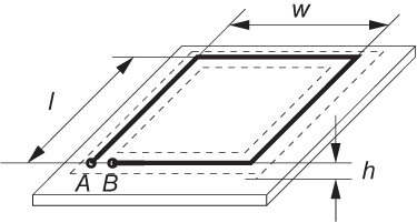
Figure 5.35 Lossy loop over a lossy ground plane.

Figure 5.36 Equivalent circuit for single-loop example.
- 5.9 Inductance of capacitor
Capacitors have multiple uses. One of the applications is as a decoupling capacitor for a power distribution network (PDN) or for power engineering applications. For this and many other applications, we need to know not only the value of the capacitor but also inductance in a connected environment. Make an (
 )PEEC model for the case shown in Fig. 5.37.
Figure 5.37 Capacitor model for inductance problem.
It is clear that the current in the capacitor will flow between the capacitor plates along the length. However, for our approximate inductance model, we assume that some connections exist between the two plates such that the inductance can be computed. In the most simple model, we assume that a short connection exists between the plates somewhere in the capacitor. Depending on the type of the capacitor, we can assume that the plates are shorted in different locations. We can assume that the short at the center of the capacitor plates is shown in capacitor cross section in Fig. 5.37.
As a second case, we can study the case where the capacitive impedance is large such that crossover happens close to the side where the B contact is located. We compute the open-loop inductance between points A and B by simply ignoring the connection to the two points. We recognize that the open-loop inductance needs to be completed with the circuit connected to the terminals to get the actual inductance value.
Assume the following dimensions:
 mm,
mm,  mm,
mm,  mm, and
  mm. For the connection wires we assume that the width
  mm, with a thickness
  mm, and the side length
  mm.
mm.
References
- 1. F. W. Grover. Inductance Calculations: Working Formulas and Tables. Dover Publications, New York, 1962.
- 2. C. Paul. Inductance, Loop and Partial. John Wiley and Sons, Inc., New York, 2010.
- 3. A. E. Ruehli. Inductance calculations in a complex integrated circuit environment. IBM Journal of Research and Development, 16(5):470–481, September 1972.
- 4. A. E. Ruehli, A. D. Ling, and A. Ruehli Eds. Circuit Analysis, Simulation and Design, Part 2. Elsevier Science Publishers B.V., North-Holland, 1987.
- 5. P. K. Wolff and A. E. Ruehli. Inductance computations for complex three dimensional geometries. In Proceedings of the IEEE International Symposium on Circuits and Systems, pp. 16–19, 1981.
- 6. M. Kamon, M. J. Tsuk, and J. White. FastHenry: a multipole-accelerated 3-d inductance extraction program. In Proceedings of the Design Automation Conference, pp. 678–683, June 1993.
- 7. C. Holloway and E. F. Kuester. Net and partial inductance of a microstrip ground plane. IEEE Transactions on Electromagnetic Compatibility, 40(1):33–45, February 1998.
- 8. A. Devgan, H. Ji, and W. Dai. How to efficiently capture on-chip inductance effects: introducing a new circuit element K. In Proceedings of International Conference on Computer Aided Design, Santa Cruz, CA, pp. 150–155, November 2000.
- 9. K. L. Shepard and Z. Tian. Return-limited inductances: a practical approach to on-chip inductance extraction. IEEE Transactions on Computer-Aided Design, 19(4):425–435, April 2000.
- 10. S. X.-D. Tan and L. He. Advanced Model Order Reduction Techniques in VLSI Design. Cambridge University Press, Cambridge, 2007.
- 11. D. Gope, A. E. Ruehli, and V. Jandhyala. Speeding up PEEC partial inductance computations using a QR-based algorithm. IEEE Transactions on Very Large Scale Integration (VLSI) Systems, 15(1):60–68, January 2007.
- 12. A. E. Ruehli Ed. Circuit Analysis, Simulation and Design, Part 2. Elsevier Science Publishers B.V., North-Holland, 1987.
- 13. C.-K. Cheng, J. Lillis, S. Lin, and N. Chang. Interconnect Analysis and Synthesis. John Wiley and Sons, Inc., New York, 2000.
- 14. G. Zhong and C.-K. Koh. Exact closed-form formula for partial mutual inductances rectangular conductors. IEEE Transactions on Circuits and Systems, 50(10):1349–1353, October 2003.
- 15. G. Antonini and A. E. Ruehli. Fast multipole and multi-function PEEC methods. IEEE Transactions on Mobile Computing, 2(4):288–298, October 2003.
- 16. A. Muesing, J. Ekman, and J. W. Kolar. Efficient calculation of non-orthogonal partial elements for the PEEC method. IEEE Transactions on Magnetics, 45(3):1140–1142, March 2009.
- 17. G. Golup and C. Van Loan. Matrix Computations. The John Hopkins University Press, Baltimore, MD, 3rd edition, 1996.
- 18. E. B. Rosa and F. W. Grover. Formulas and tables for the calculation of mutual and self-inductance. Bulletin of the Bureau of Standards, 8(1):1–237, 1912.
- 19. G. Antonini, J. Ekman, and A. Ruehli. Toward improved time domain stability and passivity for full-wave PEEC models. In Proceedings of the IEEE International Symposium on Electromagnetic Compatibility, Portland, OR, August 2006.
- 20. E. Weber. Electromagnetic Theory. Dover Publications, New York, 1965.
- 21. C. R. Paul. Analysis of Multiconductor Transmission Lines. John Wiley and Sons, Inc., New York, 1992.
- 22. A. E. Ruehli, C. Paul, and J. Garrett. Inductance calculations using partial inductances and macromodels. In IEEE Transactions on Electromagnetic Compatibility, pp. 23–28, August 1995.
- 23. C. L. Holloway, E. F. Kuester, A. E. Ruehli, and G. Antonini. Partial and internal inductance: two of Clayton R. Paul's many passions. IEEE Transactions on Electromagnetic Compatibility, 55(4):600–613, April 2013.
- 24. M. Swaminathan and A. E. Engin. Power Integrity Modeling and Design for Semiconductors and Systems. Prentice Hall, Upper Saddle River, NJ, 2007.
- 25. E.-P. Li. Electrical Modeling and Design for 3D System Integration. John Wiley and Sons, Inc., New York, Hoboken, NJ, 2012.
- 26. J. Kim, J. Fan, A. E. Ruehli, J. Kim, and J. L. Dewniak. Inductance calculations for plane-pair area fills with vias in a power distribution network using a cavity model and partial inductances. IEEE Transactions on Microwave Theory and Techniques, 59(8):1909–1924, August 2011.
- 27. F. Zhou, A. E. Ruehli, and J. Fan. Efficient mid-frequency plane inductance computations. In Proceedings of the IEEE International Symposium on Electromagnetic Compatibility, Fort Lauderdale, FL, pp. 831–836, August 2010.
- 28. L. Li, A. E. Ruehli, and J. Fan. Accurate and efficient computation of power plane pair inductance. In Proceedings of the IEEE International Symposium on Electromagnetic Compatibility, Philadelphia, PA, August 2012.
- 29. L. Wei, L. Li, K. Shringarpure, A. E. Ruehli, E. Wheeler, J. Fan, B. Archambeault, and J. L. Drewniak. Plane-pair PEEC models for power distribution networks with sub-meshing techniques. IEEE Transaction on Microwave Theory and Techniques, 64(3):733–741, March 2016.