
Chapter 8
Geometrical Description and Meshing
In this chapter, we present an overview of issues for the meshing for partial element equivalent circuit (PEEC) models. We specifically consider applications in the electromagnetic modeling (EMM), electromagnetic compatibility (EMC) areas such as interconnect modeling for power and signal integrity (SI) as well as power engineering area models. Hence, these structures include different complex mixed circuit and electromagnetic (EM) aspects. The EM structures are in general very heterogeneous and they may be connected to electronic circuits that are described in the circuit domain.
Early on in the history of PEEC models, simplified nonorthogonal geometries were modeled in terms of rectangular bars [1–4]. While the use of rectangular bars is very efficient, it also limits the geometries that can be represented with these shapes. Hence, the consistent inclusion of nonorthogonal shapes with the rectangular ones is important and evolving. In general, we need to consider a multitude of shapes for the applications of interest. Rectangular blocks are used for some parts such as printed circuit boards (PCBs) and transmission line conductors. Different round conductors are used for connection wire models of different shapes. Very thin conductors are modeled with lines or quadrilateral cells or other approximations, and volumes are represented with hexahedral models and if possible rectangular block shapes.
The solution using the Rao–Wilton–Glisson (RWG) [5] triangles is suitable for special applications. These techniques use a large number of small computationally efficient triangular cell basis functions [6] such as they are used in some integral equation modeling methods [7]. For these techniques, a larger number of smaller cells is used and the computation per cell is minimized while the number of unknowns is increased. It is clear that the use of triangular-shaped cells is a good approach for a relatively homogeneously structured high-frequency problems such as airplanes [6]. Triangles are also used in some PEEC codes, for example, Refs [9–11].
In the version of PEEC considered in this text, we avoid the use of triangular shapes. Three of the advantages are better meshing of large aspect ratio cells, the reduced number of basis functions required, and the ease of representing shallow angle structures as shown in Fig. 8.1. Another issue is the elimination of an entire set of coupling integrals and all the triangle-to-rectangle coupled elements that are needed for mixed rectangular and triangular elements. Of course, this is due to the partial or totally analytic partial elements that we prefer to use for PEEC models.

Figure 8.1 A wire section that is meshed with long, shallow angle cells.
8.1 General Aspects of PEEC Model Meshing Requirements
Today, a wide range of different meshing techniques are employed in the general area of integral equation solution techniques. An interesting set of applications consists of the modeling of antenna type structures for a multitude of shapes [12]. These applications often involve computations for a single frequency or for a limited range of frequencies. Also, these types of geometries have fewer closely spaced overlapping areas. We consider closely spaced surfaces or bodies that are in general more difficult to mesh in Section 8.4.2.
It is important to understand details of the meshing requirements for the different PEEC classes of problem. Since, overall efficiency can be gained by meshing, it is desirable to tailor the meshing part to the solution.
A simplifying issue is that we mostly address signal integrity (SI), power integrity (PI), and noise integrity (NI) problems. Usually, the accuracy of a SPICE circuit solver is in the range of ![]() to
to ![]() . This is sufficient for this class of problems. For this reason, we tailor our PEEC EM solutions in this accuracy range. One of these accuracy choices was that we considered that all cells had planar surfaces [13].
. This is sufficient for this class of problems. For this reason, we tailor our PEEC EM solutions in this accuracy range. One of these accuracy choices was that we considered that all cells had planar surfaces [13].
One of the advantages of this approach is that we can employ analytic integrations for the partial elements, which yields more flexibility. For SI/PI/NI problems, the difference in the size of geometrical objects involved can be very large. This requires additional care in choosing approximate meshes. The use of different size meshes for conductors and dielectrics needs more intelligence built into the mesher.
As shown in Section 4.4.1, the choice of the cell segmentation has a strong influence on the accuracy for closely spaced conductors as well as other objects. Hence, the meshing approach must include special techniques for closely spaced conductors or dielectrics. A technique called projection meshing must be employed. The inaccuracies introduced by close surfaces that are not meshed with projection methods were first presented in Ref. [14], and is also considered in Section 4.4.1 as well as in Refs [15–17] and [18]. Details are again considered in Section 8.4.
Nonorthogonal shapes are represented by quadrilateral surface and hexahedral three-dimensional elements. We found this to be very effective for the approximation of the currents and surface charges. Quadrilateral surface cells have been used successfully for EM modeling using integral equation solution approach, for example, Refs [19, 20].
A smart mesher can save a large number of unknowns in part due to the large cell aspect ratios that can be tolerated in PEEC due to the analytic partial elements used. This result is accomplished by the additional work, which allows much larger aspect ratios for the cells generated by the mesher. As mentioned above, triangles [5] are not used due to their sensitivity with respect to the large aspect ratios. As is shown in Fig. 8.19 we can always subdivide triangles intoquadrilateral shapes.
The parallel development of the mesher and the PEEC solver is very desirable since the mesher needs to have information about the capabilities and limitations of the solver. This implies that even at the mesher level, we have to understand more about the problems and the solution details. Some important aspects are the inclusion of both wide-band skin-effect and dielectric loss models. Another important issue is minimizing the local complexity of the meshing while preserving sufficient overall accuracy. This is somewhat different from the approach in finite element solvers where the accuracy is improved iteratively during the solution.
There are two fundamental issues that determine the size of the cells used to represent the geometry. For high-frequency or fast time domain solutions, a maximum dimension of a cell is given by ![]() where
where ![]() is the shortest wavelength in the spectrum and
is the shortest wavelength in the spectrum and ![]() , where
, where ![]() is leading generally to a good solution, at least for high-frequency problems. Hence, this may limit the maximum dimension of all cells.
is leading generally to a good solution, at least for high-frequency problems. Hence, this may limit the maximum dimension of all cells.
Second, especially for heterogeneous geometries, the sufficiently accurate representation of a current path may require even smaller cells compared to the wavelength. In the absence of other close conductors, the number of cells on conductors will be determined by the current flow or the largest frequency involved. The current flow is determined by the connections at the nodes and the required accuracy. A good aspect of the approach is that results with a reasonable accuracy can be obtained with careful meshing. It is obvious that for these cases, the use of large nonuniform cell size differences can reduce the number of cells or unknowns required in a problem.
8.2 Outline of Some Meshing Techniques Available Today
Meshing has become a separate area of research. Many different texts are available dedicated specifically to the general subject, for example, Refs [13, 21, 22]. The theory and practice of meshing are sophisticated areas. A multitude of different techniques exist today. It is useful to consider the fundamental framework for meshing, which is considered in Ref. [22], since it is relevant for our applications. It divides the techniques into three basic groups, which are outlined next.
Algebraic methods: This class of methods can be very widely interpreted. It essentially consists of meshes that are obtained with algebraic mappings. A large class of these methods are related to the nonorthogonal coordinates considered in Chapter 7. This approach is very flexible since the approach includes many different heuristic mapping methods.
PDE-based methods: In this approach, simplified partial differential equations are solved. For example, solution to Laplace's equation is used for meshing details inside the region of interest. Often, we see approaches that may be in part algebraic and also based on partial differential equation (PDE) solutions.
Multiblock methods: Multiblock methods break up the overall region or problem into subproblems that are solved somewhat separately. Of course, they have to match at the boundaries. These methods are of importance for our class of problems. They often consist of different elements that are best considered as separately meshed areas. Ultimately, the matching of the different parts has to be consistent. Some of these issues are considered in this chapter.
8.2.1 Meshing Example for Rectangular Block
First, we give a fundamental example of a PEEC mesh. It is best to start from the most simple case, which is a thin, rectangular sheet as we considered in the previous two chapters. Of course, we used simple PEEC meshing examples previously starting with Chapter 2. Unfortunately, most real-life examples are more complicated than what we have considered so far.
We use the simple example in Fig. 8.2 for a thin sheet of metal. Also, we assume that it exists in free space without the presence of other conductor or dielectric objects in its vicinity.

Figure 8.2 Inductive and capacitive mesh for sheet or block.
Some of the inductive/resistive cells are shown in Fig. 8.2a, whereas some of the capacitance cells are shown in Fig. 8.2b. We use half cells at the edge for both the inductive and the capacitive cells. The advantage of this is that this object can be connected at the nodes. Then two touching half cells can connect into full cells. Hence, we have a flexible approach where structures can be built from blocks that connect together in a systematic way. Again, for clarity, not all the inductive cells connected to a node are shown. For example, in Fig. 8.2a, four partial inductances are connected to node 4. As is apparent from Fig. 8.2b, we also connect a capacitive surface cell to the node on both the upper and the lower surfaces.
Internal nodes of a thick conductor block or brick will not have capacitive cells associated with them. In Section 6.3.2, it was shown that the internal charge is zero. However, in the volume filament (VFI) model considered in Chapter 9, the internal nodes represent a key contribution to the skin-effect model.

Figure 8.3 Inductance volume cells for rectangular conductor.
Figure 8.3 together with Fig. 8.2 can be considered the complete meshing for a rectangular block where all six faces have surface cells such as the ones shown in Fig. 8.2b. Hence, the cube example has four nodes in the ![]() -direction, three nodes in the
-direction, three nodes in the ![]() -direction, and four nodes in the
-direction, and four nodes in the ![]() -direction, and the block or brick has a total of 48 nodes.
-direction, and the block or brick has a total of 48 nodes.
Finally, we give a 3D meshing example to illustrate the half and quarter cells at the corner in Fig. 8.4. The purpose of this example is to illustrate some of the cells involved at the corner of a conductor or dielectric block.
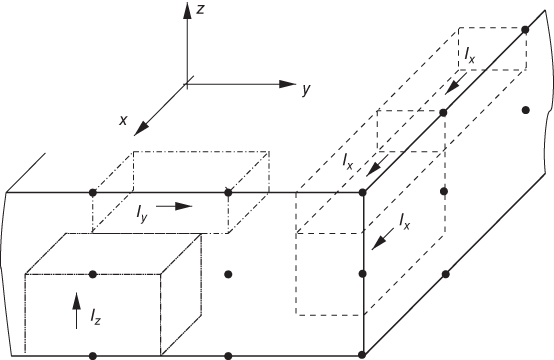
Figure 8.4 3D meshing of a corner for finite thickness plane.
8.2.2 Multiblock Meshing Methods
We start out with the concept of multiblock meshing [22] outlined above. This is clearly a top-down hierarchical approach. We may have important details that we can give to the mesher, for the specific problem about the subblocks at hand. This may help to break up the problem into multiple domains that are meshed separately in detail. The connection between the sections is accomplished by connecting appropriate nodes as is illustrated in the previous section.
The meshing of subproblems is generally much less complex than the meshing of the total problem. Hence, wherever possible, we subdivide our problems into sections. An obvious example for using is a connector where different parts of the system are designed separately before being connected together. However, an overall model may need to include such parts as a connector. This may be the starting point for partitioning into different mesh subsections. The reduction of the overall complexity by this approach may be substantial.
8.2.3 Meshing of Nonorthogonal Subproblems
The meshing of subregions is, in many cases, constrained by the boundary regions. It is clear that each subregion needs to exhibit the appropriate boundary nodes to share with other subsections by coinciding nodes. First, we have to find the appropriate constraints for the location of all boundary nodes.
Again, each subcell at the interface is designed to be flat. We give in this section an example for a quad that is located in the ![]() plane. The global corners are given in Table 8.1.
plane. The global corners are given in Table 8.1.
Table 8.1 Global corner specification for quadrilateral block surface example.
| Corner number | |||
| 0 | 1 | 1 | 0 |
| 1 | 1.5 | 3 | 0 |
| 2 | 2.5 | 0.8 | 0 |
| 3 | 2 | 3.2 | 0 |
To submesh the quad-block into suitable subquads and cells for the PEEC model, we simply apply (7.5) for the mapping of the ![]() and
and ![]() locations. Hence, the nodes of the subcircuit are given by choosing
locations. Hence, the nodes of the subcircuit are given by choosing ![]() and
and ![]() as
as ![]() . The result for the submesh is shown in Fig. 8.5 which was created with a small Matlab program. To obtain this model a single plane piece shown in Fig. 7.5, Section 7.2, is used by laying out with subdivisions. Also shown in Fig. 8.5, is an example of local coordinate labels to the internal nodes are further used in sections 8.2.5 and 8.3.
. The result for the submesh is shown in Fig. 8.5 which was created with a small Matlab program. To obtain this model a single plane piece shown in Fig. 7.5, Section 7.2, is used by laying out with subdivisions. Also shown in Fig. 8.5, is an example of local coordinate labels to the internal nodes are further used in sections 8.2.5 and 8.3.

Figure 8.5 Submeshing for a flat nonorthogonal quadrilateral block patch.
8.2.4 Adjustment of Block Boundary Nodes
In order to connect two different blocks together, the nodes of all of the block boundaries need to be adjusted or its number increased or reduced. It is clear that if we have a mosaic of different blocks, we have to match all the nodes to the adjoining boundary nodes. Fortunately, techniques exist for the change in boundary node locations. Examples are available, for example, Ref. [23]. In Fig. 8.6, we give an example where two additional nodes are introduced between the global nodes 2 and 3. Of course, the subquads generated by this process need the labeling of the new quads and nodes in the global coordinates.

Figure 8.6 An example for the introduction of additional boundary nodes.
It is obvious that additional nodes are added at the side of the boundary where they are necessary.
8.2.5 Contacts Between the EM and Circuit Parts
Contacts must be made between the different blocks for a multi-block environment. The entire problem, including the EM parts is solved as a single problem in the time or frequency domain solution.
It is evident from the previous section that the connection to a geometrical element can be established at each of the electrical nodes of a body. Each node is labeled by a specific location in terms of the local ![]() coordinates shown in Fig. 8.5 for the block. An example is
coordinates shown in Fig. 8.5 for the block. An example is ![]() ,
, ![]() , and
, and ![]() . These coordinates are unlike the usual local coordinates. Rather, they represent integer coordinates that enumerate the nodes along each side of a body, which may consist of multiple cells. As an example,
. These coordinates are unlike the usual local coordinates. Rather, they represent integer coordinates that enumerate the nodes along each side of a body, which may consist of multiple cells. As an example, ![]() means the first node along the
means the first node along the ![]() side. The
side. The ![]() notation is used instead of
notation is used instead of ![]() since the overall body may not be Manhattan brick shaped. An example of the joining of nodes is shown in Fig. 8.10.
since the overall body may not be Manhattan brick shaped. An example of the joining of nodes is shown in Fig. 8.10.
It is still not trivial to correctly connect the electrical circuit to the electromagnetic model. Inaccuracies may occur near the connections. For example, a wire contact attached to a conducting body as shown in Fig. 8.7a may create a large number of cells and unknowns. However, this can be avoided with clever approximations. If we attempt to replace the contact with a single wire macromodel, as shown in the example in Fig 8.7b, then the contact area must be chosen to be large enough as is shown by the dashed area in Fig. 8.7b.
Essentially, the contact modeling is not trivial. Often an insufficient number or too many cells are used in the models of the details of the connections. The size of the contact is not defined by the conductor and the size and the resistance will increase with cell refinements. To avoid this, we have to use a cell with a fixed size with the wire cross section shown by dashed lines in Fig. 8.7b. Hence, the connection size could be locally defined independent of the number of surrounding cells used for the mesh.

Figure 8.7 Contact and macromodel for contact.
This is an example that shows that care must be taken when more efficient, simplified models are used. A similar simplifying technique can be used for a wire which is a via connection through a plane which does not make a connection to this plane as is considered in Fig. 8.17. In fact, for a very simple model, a wire can connect through a ground plane where we completely ignore the presence of a hole in the plane through which the wire is connected.
8.2.6 Nonorthogonal Coordinate System for Geometries
The basis of the meshing consists of the description for the conductor, dielectric as well as other objects such as sources, loads, and potentially connected integrated and other circuits. We suggest that the reader reviews Section 7.1, as an introduction to the relation of the local coordinates (a, b, c) to the global system ![]() .
.

Figure 8.8 Basic quadrilateral object with local coordinates.
Three-dimensional geometries with an arbitrary orientation represent an important case. Fortunately, this is just an extension of the case in (7.1) represented in (7.2). We consider the case in Fig. 8.8 that consist of a zero thickness quadrilateral shape. In fact, the more general quadrilateral shape in Fig. 8.9 also includes a potentially variable thickness of the shape by adding a ![]() coordinate where
coordinate where ![]() much like the
much like the ![]() and
and ![]() variables. The equations for this case are
variables. The equations for this case are

The coordinate system used for a hexahedral element is shown in Fig. 8.9. Again, the local coordinates identify the location of any point belonging to the hexahedron in terms of variables ![]() where
where ![]() , where
, where ![]() represents
represents ![]() , or
, or ![]() . The purpose of all this is to uniquely map a coordinate
. The purpose of all this is to uniquely map a coordinate ![]() into a point in the global coordinates
into a point in the global coordinates ![]() . We accomplish this by interpolating a point vector from eight point vectors
. We accomplish this by interpolating a point vector from eight point vectors ![]() where
where ![]() with the coordinates
with the coordinates ![]() . It will be clear that the corners of the hexahedron are reached when
. It will be clear that the corners of the hexahedron are reached when ![]() .
.

Figure 8.9 Basic hexahedral element or object with local coordinates.
We use the same node assignment as presented in Table 7.1. This creates an assignment of the orientation of the quadrilateral of hexahedral surfaces in the mesh as shown in Fig. 8.9 for the hexahedron using the binary code for the symbols ![]() , where the
, where the ![]() coordinates map into logical zeros, and +1 coordinates map into logical ones. The order of the logical variables is
coordinates map into logical zeros, and +1 coordinates map into logical ones. The order of the logical variables is ![]() . Hence, for example, the binary code
. Hence, for example, the binary code ![]() corresponds to the corner
corresponds to the corner ![]() ,
, ![]() , and
, and ![]() and its decimal equivalent is 3 for corner 3 as can be verified in Fig. 8.9. This makes the assignment unique and easy to remember. As indicated above, all local coordinates have to relate back to the global
and its decimal equivalent is 3 for corner 3 as can be verified in Fig. 8.9. This makes the assignment unique and easy to remember. As indicated above, all local coordinates have to relate back to the global ![]() coordinates. Therefore, a unique representation is needed for the mapping from a local point
coordinates. Therefore, a unique representation is needed for the mapping from a local point ![]() on an object to the global point
on an object to the global point ![]() . Mapping a point in the above hexahedron from a local coordinate point
. Mapping a point in the above hexahedron from a local coordinate point ![]() into a global coordinate point
into a global coordinate point ![]() is described by (7.3) as
is described by (7.3) as


The coefficients in (8.2) are given by (7.4) where ![]() and again
and again ![]() . The close relation to the binary variables is evident.
. The close relation to the binary variables is evident.
With this, we are in a position to also express the tangential vectors with respect to the local coordinates as
where the derivatives are found from (8.2a) as presented in detail in Section 7.1.2. Finally, the magnitude of the tangential vector ![]() where the position-dependent unit vectors can be determined from
where the position-dependent unit vectors can be determined from ![]() where again
where again ![]() . With this, we are prepared to formulate the geometrical aspects for the nonorthogonal PEEC circuit elements.
. With this, we are prepared to formulate the geometrical aspects for the nonorthogonal PEEC circuit elements.
8.3 SPICE Type Geometry Description
In the PEEC circuit solution, terminal or nodal variables are associated with each of the resultant circuit elements. They will be collected in the modified nodal analysis (MNA) circuit solver part in the vector of unknowns. The solution vector variables are quantities such as the potentials ![]() , and other conventional circuit variables such as
, and other conventional circuit variables such as ![]() where
where ![]() is the current,
is the current, ![]() is the voltage, and
is the voltage, and ![]() is the charge, if necessary. If no other circuit elements are included, the solution vector
is the charge, if necessary. If no other circuit elements are included, the solution vector ![]() is used as the only unknown since this vector directly yields the most useful EM circuit output variables.
is used as the only unknown since this vector directly yields the most useful EM circuit output variables.
The general PEEC model can involve conventional lumped circuit elements as well as physical shapes as shown, for example, in Fig. 8.5. Hence, the question is if we could describe the geometrical objects using the SPICE circuit language such that the connection between the SPICE circuit elements and the geometrical objects can directly be established.
As is evident from the above representation of quadrilateral surfaces or the hexahedral blocks can be used as the geometrical units. In most cases, amultiblock-type mesh description of the geometry is suitable. Also, we subdivide mixed circuits and EM problems including the connections between the problem domains.
In the circuit domain, the SPICE language is used for the circuit description as a standard. Unfortunately, the details of the language are not well standardized while the SPICE language is used in numerous circuit solvers using subcircuits to describe blocks of circuits.
In a multiblock geometrical meshing environment, we can also create meshed parts that correspond to the subcircuits in the circuit domain. Hence, finite conductor and dielectric blocks can be implemented for the general combined orthogonal and nonorthogonal three-dimensional geometries. Two basic statements are used in a form that is compatible with hexahedral structures for the nonorthogonal PEEC approach [17].
An interesting simplification for the description file for the geometry can be achieved for problems of interest. Conventionally, the shapes of the partial elements are described by the geometry files, a shape at the time. This means that each cell for the partial elements is described by a single statement. However, we can also describe geometrical objects that include multiple partial elements or cells. Specifically, the geometrical section shown in Fig. 8.9 can be a unit that later will be modeled in terms of the partial elements. An example of the labeling of the subdivisions is given in Fig. 8.5 and it is used in this section.
An important aspect of the joined geometry-circuit description is the identification of the nodes that are well defined for the PEEC cells and the nodes can be uniquely labeled. Hence, SPICE circuit elements can be connected to the nodes.
The labeling of nodes is rather simple. The nodes of a block can uniquely be identified by the block number and the node identified by the three dimensions ![]() , or
, or ![]() , which may correspond to
, which may correspond to ![]() for orthogonal shapes. Hence, for a block, the number of subdivisions can be specified by the number of subdivisions in each direction for the block as
for orthogonal shapes. Hence, for a block, the number of subdivisions can be specified by the number of subdivisions in each direction for the block as ![]() ,
, ![]() and
and ![]() . Hence, the cell subdivision nodes can uniquely be specified starting at the corner
. Hence, the cell subdivision nodes can uniquely be specified starting at the corner ![]() , and so on. The label for the node at the corner would be
, and so on. The label for the node at the corner would be ![]() . Hence, the label for the next nodes along the
. Hence, the label for the next nodes along the ![]() edge could be
edge could be ![]() .
.
Finally, the description of a block conductor with a conductivity ![]()
![]() or also
or also ![]() .
.
.pr1 ADIV=2 BDIV=3 CDIV=1 RhoV=1.724e-8Ohm*m
.Bh1 pr1 0mm 0mm 0mm
         0mm 1mm 0mm
         2mm 0mm 0mm
         2mm 3mm 0mm
         0mm 0mm 7mm
         0mm 1mm 0mm
         2mm 0mm 7mm
         2mm 3mm 7mm
The ![]() information specifies the properties of the body and the
information specifies the properties of the body and the ![]() uses the
uses the ![]() statement and the coordinate points for the eight vertices of a hexahedral body, where the
statement and the coordinate points for the eight vertices of a hexahedral body, where the ![]() of the global coordinates are given.
of the global coordinates are given.
8.3.1 Shorting of Adjoining Bodies
Most multiblock elements are connected to other ones to construct large geometries. The connection nodes to the body are uniquely defined in the above example where a connection is possible at each of the nodes defined above. It is clear that nodes of the neighboring conductors should be at matching physical location within a tolerance as is considered in Section 8.4.4. Electrically, the bodies are connected by joining nodes as shown in Fig. 8.10. A SPICE-type statement is used to indicate the shorting process in the input file. An example of a shorting SPICE-type statement is
.short Bh1(A0,B1,C1) Bh2(A0,B0,C1)for one connection in the back of the body. This will hide some inside surfaces once the two bodies in Fig. 8.10 are merged. These surfaces will be declared to be charge free.

Figure 8.10 Example of shorting between two hexahedral bodies.
8.4 Detailed Properties of Meshing Algorithms
The size of the PEEC surface or volume mesh may be limited by other constraints. For example, a given cell ![]() , which may represent a partial inductance or a potential coefficient, which has a diameter
, which may represent a partial inductance or a potential coefficient, which has a diameter ![]() defined by
defined by ![]() , where
, where ![]() are the diagonals of a cell. The size of the mesh cells is clearly determined by two different issues: (a) the fact that the diameter should not exceed the
are the diagonals of a cell. The size of the mesh cells is clearly determined by two different issues: (a) the fact that the diameter should not exceed the ![]() for high-frequency impedance problems; and (b) by the sufficient details of the representation of the current or charge distributions.
for high-frequency impedance problems; and (b) by the sufficient details of the representation of the current or charge distributions.
The current distribution issue is sometimes called the Laplace factor since it may locally be the local solution of a PDE [22], which could be the Laplace equation. The solution to Laplace equation can be useful in the determination of locally dense conductor situations. Meshes such as the one in Fig. 8.1 result where the current flow is taken into account by the mesh.
The appropriate mesh size is a combination between the two factors considered in the previous two paragraphs. Of course, from an efficiency point of view, we would like to make the cells as large as possible. However, the size of the mesh cell is limited by the smaller of the two criteria – possibly in all three spatial directions.
For PEEC, we also assume that some of the mesh cells may have a very large aspect ratio ![]() in the different spatial directions
in the different spatial directions ![]() or
or ![]() for rectangular cells. For example, for a zero thickness rectangular cell, we define the aspect ratios as
for rectangular cells. For example, for a zero thickness rectangular cell, we define the aspect ratios as ![]() . The exact definition of large depends on the problem details. As two examples, a large aspect ratio can be
. The exact definition of large depends on the problem details. As two examples, a large aspect ratio can be ![]() and
and ![]() or
or ![]() and
and ![]() . Similarly, for nonorthogonal shapes, we can use the distance, for example, in the
. Similarly, for nonorthogonal shapes, we can use the distance, for example, in the ![]() direction by taking the distance corresponding to the points
direction by taking the distance corresponding to the points ![]() and
and ![]() , which maps to the global (
, which maps to the global (![]() ) coordinates map to using (8.1)
) coordinates map to using (8.1) ![]() . Then, the distance ratio of interest may be
. Then, the distance ratio of interest may be ![]() with the length
with the length ![]() defined in the same way. Again, the relevant aspect ratios that need to be computed depend on the problem details.
defined in the same way. Again, the relevant aspect ratios that need to be computed depend on the problem details.
The ratio ![]() may also be limited by the quality of the implementation of the partial element integrals considered in the Appendices C–E. Partial elements need to be optimized such that they remain accurate even for very large aspect ratio cells while not resulting in large compute times. This is discussed in Section 5.5.2 for inductances.
may also be limited by the quality of the implementation of the partial element integrals considered in the Appendices C–E. Partial elements need to be optimized such that they remain accurate even for very large aspect ratio cells while not resulting in large compute times. This is discussed in Section 5.5.2 for inductances.
The meshing needs to be surface and volume compatible since we want to use the meshing for combined volume (V)PEEC and surface (S)PEEC and combined (V,S)PEEC [24] models. Fortunately, the theory for quadrilateral and hexahedral meshing is well developed today, for example, Refs [25–28]. Hence, we can benefit directly from this large body of work.
8.4.1 Nonuniform Meshing Algorithm for Efficient PEEC Models
Nonuniform mesh layers are used for efficient skin-effect models as is shown in Chapter 9. Examples of skin-effect models with variable thickness layers are given in Ref. [29]. It was also shown that efficient capacitance models can be constructed using nonuniform mesh sizes, for example, Ref. [30]. Further, in for example Ref. [31], better results were obtained if the cell sizes were decreased toward the ends of a transmission line structure. However, we need to observe that nonuniform cells may be constrained by other meshing requirements such as projection requirements. These issues are considered below.

Figure 8.11 Example of conductive sheet of thickness 2D with skin-effect layers.
We consider the layer or mesh thickness of the nonuniform skin-effect models. This is used in several models presented in Chapter 9. We assume that the problem starts with a conducting layer as shown in Fig. 8.11.
In general, we assume that the conductor has a finite thickness and we are meshing it symmetrically toward the center. This assumes that we care about the current flow on both sides of the conducting sheet. We can adjust the meshing to other situations. For example, we may have transmission lines only on one side of the conducting layer or ground plane. In this case, we need the mesh refinement only on one side of the conductor.
Next, we consider how the layer thickness in Fig. 8.11 is subdivided. For this reason, we consider the thickness direction in more detail as shown in Fig. 8.12.

Figure 8.12 Example mesh for increasing layer thickness.
Without loss of generality, we assign ![]() to the thickness variable direction. Usually, the thin first layer is chosen to be smaller than the skin-depth
to the thickness variable direction. Usually, the thin first layer is chosen to be smaller than the skin-depth ![]() at the highest frequency [29]. This layer has the thickness
at the highest frequency [29]. This layer has the thickness ![]() in Fig. 8.12.
in Fig. 8.12.
As is presented in Chapter 9, the current density decays away from the surface. A compromise between the minimum number of layers and the model accuracy determines the increase ![]() , which is the factor by which the thickness of the layer is increased in comparison to a previous layer.
, which is the factor by which the thickness of the layer is increased in comparison to a previous layer.
In (8.4), we compute the location of the layers, starting at the surface of the conductor toward the center.


The goal is to subdivide the conductor with a reasonable number of cells or layers while keeping the increase in the layer thickness ![]() such that it provides a reasonable accuracy. Also, the number of layers should be as small as possible, such as
such that it provides a reasonable accuracy. Also, the number of layers should be as small as possible, such as ![]() . We should note that the exponential increase in the layers can rapidly result in large overall conductor thickness. Else, the factor
. We should note that the exponential increase in the layers can rapidly result in large overall conductor thickness. Else, the factor ![]() for the center thickness of the conductor can be increased.
for the center thickness of the conductor can be increased.
From (8.4), we can add the total thickness of all layers as
Hence, this is

where the last expression is the usual sum for a geometric series.
Using (8.6), we can find a compromise between the number of layers ![]() and the thickness of the thin layer
and the thickness of the thin layer ![]() as well as the increase in the layer thickness
as well as the increase in the layer thickness ![]() . Several examples of layered models are given in the following chapter.
. Several examples of layered models are given in the following chapter.
The consequence of nonuniform meshing can be the creation of cells that are too large due to the fast increase in the layer thickness. This may result in a maximum cell size condition ![]() . The parameters of the algorithm such as
. The parameters of the algorithm such as ![]() can be adjusted in the limit value of the maximum cell size.
can be adjusted in the limit value of the maximum cell size.
Also, for very thick conductors, we may want to model the center of a conductor with uniform cells once a certain layer thickness has been reached.
8.4.2  Cell Projection Algorithm
An important issue has led to the ![]() cell projection algorithm. It was recognized early on that the cells between closely overlapping conductors must be lined up or projected on each other. It was shown in Ref. [14] that poor results are obtained if nonprojected cells are used. The same issue is also substantiated in Section 4.4.
cell projection algorithm. It was recognized early on that the cells between closely overlapping conductors must be lined up or projected on each other. It was shown in Ref. [14] that poor results are obtained if nonprojected cells are used. The same issue is also substantiated in Section 4.4.

Figure 8.13 Example of  -projection for layers under narrow conductor.
We consider the realistic example where several layers are located in close proximity to a narrow conductor. The boundaries for all closely located cells need to be lined up. This is even more difficult to accomplish for a conductor or dielectric with other closely located bodies on both sides. The cells on both sides need to be closely projected on each other. It becomes even more complicated for multiple close layers where the cell size should be different on both sides of layers. For this case, it is desirable to attempt a slow increasing or decreasing in the projection between the cell boundaries. We call the technique used for the cell size change ![]() -projection algorithm. The motivation is given by a permissible angle
-projection algorithm. The motivation is given by a permissible angle ![]() by which the cell size projection changes.
by which the cell size projection changes.
We illustrate the ![]() projection issue in Fig. 8.13, where it is required that the cell width at the bottom surface should be larger than the small width
projection issue in Fig. 8.13, where it is required that the cell width at the bottom surface should be larger than the small width ![]() of the top conductor. This is accomplished by increasing the cell width for each layer in Fig. 8.13 to
of the top conductor. This is accomplished by increasing the cell width for each layer in Fig. 8.13 to ![]() . For the layer that is at distance
. For the layer that is at distance ![]() from the narrow top conductor, the cell width is increased to
from the narrow top conductor, the cell width is increased to
It is clear that fewer unknowns result if larger cells can be used. Experimentally, the best results have been obtained where the angle ![]() is somewhat increased with distance
is somewhat increased with distance ![]() in the example in Fig. 8.13, rather than being the same for all layers.
in the example in Fig. 8.13, rather than being the same for all layers.
Another issue related to the example in Fig. 8.13 is that conductors also need to be subdivided along the cell width ![]() . This represents the fact that the current also distributes toward the edge of the conductor. To accomplish this, further width subdivisions may be needed for the conductor with the overall width
. This represents the fact that the current also distributes toward the edge of the conductor. To accomplish this, further width subdivisions may be needed for the conductor with the overall width ![]() . This is part of the VFI skin-effect model in Section 9.3. Hence, it would be very costly to also project the small width of the cells to the layers.
. This is part of the VFI skin-effect model in Section 9.3. Hence, it would be very costly to also project the small width of the cells to the layers.
Provided that we want to use nonorthogonal cells, we can use the node matching technique in Fig. 8.14 to eliminate as many small cells as possible. Of course, we want to use quadrilateral or hexahedral cell for the transition. The assumption for this approach is that the thickness of the layers below is not small compared to the spacing of the subdivision of the conductor of total width ![]() . It is evident that the spacing of the nodes cannot be changed much since it is important to maintain a moderate side-to-side projection ratio.
. It is evident that the spacing of the nodes cannot be changed much since it is important to maintain a moderate side-to-side projection ratio.

Figure 8.14 Reduction of four nodes (top) to three nodes (bottom) surfaces.
8.4.3 Smoothing and Tolerancing
Other well-known processing steps performed on existing or new mesh structures are smoothing and tolerancing. The ultimate goal of this is again to reduce the number of unknowns with little loss of accuracy. In these approaches, the meshes are changed and the geometrical objects may be slightly approximated to simplify the meshing. In some large aspect ratio cases, the goal is to use as many rectangular or cubical cells as possible since they are computationally more efficient. In some cases, this results in a considerable reduction of the number of unknowns, which can also help to simplify the joining of the different multiblock parts.
A nontrivial aspect is to determine the error that results from the slight change in the geometry due to the tolerance in the geometry. It is clear that the geometrical changes must be very small compared to the shortest wavelength corresponding to the highest frequency. Also, the current flow should not be significantly altered. The low-frequency current flow is especially important in PEEC solutions since the same solver can be employed for very low frequencies that include the dc solution.
8.4.4 Node Relaxation
Several techniques can be used to simplify the meshing problem. We can associate a tolerance sphere for each node, which is called the node relaxation approach. In this approach, nodes within the particular tolerance spheres will be connected together.

Figure 8.15 Example for node joining with tolerance circle test.
This is illustrated in Fig. 8.15, where the two left nodes 1 and 2 are shorted together since the tolerance spheres are overlapping. On the right side of Fig. 8.15, we show that nodes 3 and 4 are too far apart to be connected since the tolerance spheres do not overlap. The equivalent circuit for the shorted nodes can be simplified by joining partial elements. In fact, this simplification is also used in the joining of multiblocks in Section 8.3.1.
Next, we illustrate some applications of node relaxation-based tolerances. The node shift or relaxation leads to larger approximations for coarse meshes and objects since the tolerance sphere should be proportional to the mesh size.
A first application example relates to electrical connections and measuring probes. Some of these probes have given geometrical distances between the contacts. Electrical probes or contacts can be used to observe port voltages or currents. Also, electrical current or voltage type sources are used to apply currents or voltages to the physical structures or to connect general SPICE-type equivalent circuits to the electromagnetic geometries. Using tolerance circles or spheres will make it easier to place the contacts to a more uniform mesh to the PEEC mesh.
We give a second example for the use of approximate models. We often need solution for package models to study the overall long-time behavior. However, for these long-time solution the waveform details are less important For this case, it is desirable to decrease the meshing accuracy by switching to a coarser mesh. For a more coarse mesh, we found that it is easier to use the node positioning relaxation algorithm to let the contacts, etc., snap to locations in the new mesh. Usually, the simplified mesh leads to considerably reduced compute times.

Figure 8.16 Node relaxation with rectangular cells.
For the third application, we return to the ![]() -projection technique given in the previous section in Fig. 8.13. However, if the layers are approximated by rectangular type cells, the application of node relaxation can be used if the angle
-projection technique given in the previous section in Fig. 8.13. However, if the layers are approximated by rectangular type cells, the application of node relaxation can be used if the angle ![]() is small. In Fig. 8.16, we give an example where the tolerance spheres are overlapping such that the nodes are connected together.
is small. In Fig. 8.16, we give an example where the tolerance spheres are overlapping such that the nodes are connected together.
8.5 Automatic Generation of Geometrical Objects
The mesh generation in this section consists of several examples. Hopefully, it provides the fundamental concepts for the generation of geometrical objects.
We start out with a simple example. Today's PCBs have many layers. This implies that multiple via connections and decoupling capacitors are involved. Simplifications can be built into PEEC model meshing. In this example, a via connection between the points A and B as shown in Fig. 8.17 has not to be connected to the center plane at the via connection location.

Figure 8.17 Via connection without meshed hole in plane.
For low frequencies, the impact on the unconnected plane can be ignored. This is considered in Section 8.2.5. On the other hand, the connection between the upper and lower conductors can be established in the circuit domain by replacing the connection with a short circuit or a small macromodel such as a resistor in series with a partial inductance connected between node points A and B. It is clear that the meshing of plane in the middle is simplified considerably by approach.

Figure 8.18 Zero thickness approximation of an L-shaped 3D object.
8.5.1 Automatic Meshing Techniques for Thin and Other Objects
Physically thin conductor can be represented by a zero thickness meshing approximation. The key issue clearly is the joining of the thin planes as shown in Fig. 8.18. Further approximations can be made later by adding some thickness in the PEEC plane models. For the meshing, the planes are replaced by zero thickness planes located at the center of the actual conductor thickness as shown in Fig. 8.18. The planes need to be connected at the intersection where the nodes from both planes are connected. Importantly, the dominant physics and circuit properties are preserved by this simplification.
Today, different techniques exist for the meshing of complex geometries. Among the techniques for mesh generation, a distinction has been made between Indirect Methods and Direct Methods.
The first indirect approach generates the quadrilateral surfaces by starting from an initial triangular mesh (e.g., Delaunay [22]). Quadrilateral shapes are then created inside the triangles. This approach is simple, robust, and well established. The easiest way to generate quadrilateral shapes is to subdivide each triangle into three quadrilaterals with the center points of the three sides as vertices and a barycenter of neighboring triangles, as shown in Fig. 8.19.

Figure 8.19 Triangle to quadrilateral subdivision.
The second class, called direct methods, creates quadrilaterals directly without using an initial geometrical decomposition. This increases the control over the shape of the individual quadrilaterals. It is always desirable to create rectangular type shapes where possible. The obvious reason for this is the parameters associated to rectangles can be computed efficiently and accurately. Also, rectangular shapes allow very long cells, which is useful for efficiency improvements.
An example of a meshed thin metal structure is given in Fig. 8.20.

Figure 8.20 Example of small thickness meshed structure EMC problem.
The quality ![]() of a mesh can be defined as
of a mesh can be defined as

where ![]() is the
is the ![]() th angle of the
th angle of the ![]() th quadrilateral,
th quadrilateral, ![]() is its area, and
is its area, and ![]() is the total number of quadrilaterals.
is the total number of quadrilaterals.
The direct methods provide meshes of higher overall quality than indirect methods. The issues of interest are execution time, quality of the mesh, and total number of quadrilaterals created. Some of the direct methods of interest are the looping algorithm, the domain decomposition through geometric optimization, and bubble mesh. We only briefly consider the principles of the looping algorithm.
8.5.2 Looping Algorithm Example
To illustrate some of the techniques used, we give a short introduction into the so-called looping algorithm. Sluiter and Hansen [32], as well as Talbert and Parkinson [33], have developed a recursive algorithm for the decomposition of a planar domain into quadrilateral shapes.
It starts out with a planar domain with a fixed contour, which consists of piecewise linear segments as shown in Fig. 8.18. The required mesh density is prespecified according to some local requirements. Hence, it starts out with the closed polygonal made of ![]() nodes and
nodes and ![]() edges.
edges.
At each step, the algorithm subdivides the oval polygon through a segment (known as split line) of length ![]() , where the ends connect to two of the
, where the ends connect to two of the ![]() nodes as shown in Fig. 8.21. Other quantities needed in the algorithm are the length of the polynomial diagonal
nodes as shown in Fig. 8.21. Other quantities needed in the algorithm are the length of the polynomial diagonal ![]() as well as the two areas of the subdomains
as well as the two areas of the subdomains ![]() and
and ![]() and the four angles 1–4 shown in Fig. 8.21.
and the four angles 1–4 shown in Fig. 8.21.
Chae and Jeong proposed in Ref. [34] to associate each possible split line with a value that takes all the abovementioned parameters. The best split line is identified as minimizing a function that is empirically obtained as combination of all the previous defined parameters. Recursively subdividing the original domain in subdomains leads to obtain polygons with four, six, or eight sides. In our case, quadrilaterals are directly obtained.

Figure 8.21 Examples of possible split line.
8.6 Meshing of Some Three Dimensional Pre-determined Shapes
A technique that has proven to be successful in commercial EM solvers is the generation of common physical shapes. Some fundamentals for such an approach given here are based on the work in Refs [23, 35]. These authors call a generator of such a shape a generatrix. For compatibility reasons, we also will adhere to their other assigned names with slight additions. They are as follows:
- BodRev This represents bodies of revolution. This represents a class of special shapes or generatrices like a circle that can be created by a rotation.
- BodTrans Such a body is created by the translation of another body or generatrix.
- BodTwoGen This body is generated by the use of two generatrices. An example is a tube created by meshing two circles.
Many complex structures can be modeled by quadrilaterals and seven hexahedral shapes can be made by combining generatrices and the use of two generatrices (BodTwoGen). Differently shaped bodies can be obtained from two generatrices. The two BodRev shapes do not exactly have to be the same.
As we show, models of circles, arcs, ellipses, squares, rectangles, and spirals can be created. Thus, simple but fairly general algorithms for geometrical modeling can be obtained. For example, a circular waveguide and coaxial lines can be modeled with BodRev shapes. Structures can efficiently be modeled by combining a spiral quadric generatrix and a body of two generatrices BodTwoGen [23].
8.6.1 Generation Techniques and Meshing of Special Shapes Like Circles
We briefly consider the generation of the meshing of special shapes such as circles. This is the generatrix according to the work in Ref. [35]. A function for circular shapes is based on the familiar equations for circles and ellipses.

where ![]() and
and ![]() represent length dimensions of the main axes along
represent length dimensions of the main axes along ![]() - and
- and ![]() -coordinates, and the parameter
-coordinates, and the parameter ![]() determines the general shape of this function. For example, a circle or ellipse is obtained for
determines the general shape of this function. For example, a circle or ellipse is obtained for ![]() , a rectangle is obtained in principle for
, a rectangle is obtained in principle for ![]() , and a rhomboid is obtained for
, and a rhomboid is obtained for ![]() . In order that arcs and spirals can also be defined, (8.9) is modified into the spiral quadratic function, described by the following parametric equations
. In order that arcs and spirals can also be defined, (8.9) is modified into the spiral quadratic function, described by the following parametric equations
where ![]() is a scale factor.
is a scale factor.

Figure 8.22 Example node point arrangements created by generatrix equation.
The parameter ![]() is an angle measured from the
is an angle measured from the ![]() -coordinate axis and takes values from
-coordinate axis and takes values from ![]() to
to ![]() . If
. If ![]() various types of arcs are obtained. If
various types of arcs are obtained. If ![]() is different from zero and
is different from zero and ![]() , different spiral functions are obtained.
, different spiral functions are obtained.
A generatrix will be used as a basis which gives the quadrilaterals to place the PEEC models. Positions of the nodes are defined by angles ![]() :
:
where ![]() is the number of nodes.
is the number of nodes.
We chose ![]() for all the experiments presented below. Three examples are shown in Fig. 8.22 for the application of (8.11). The parameters in the
for all the experiments presented below. Three examples are shown in Fig. 8.22 for the application of (8.11). The parameters in the ![]() case are
case are ![]() ,
, ![]() ,
, ![]() , and for
, and for ![]() nodal points. For the
nodal points. For the ![]() , the parameters are
, the parameters are ![]() ,
, ![]() ,
, ![]() , and
, and ![]() nodal points. Finally, for the Semicircle
nodal points. Finally, for the Semicircle ![]() ,
, ![]() ,
, ![]() , and
, and ![]() nodal points only.
nodal points only.

Figure 8.23 Spiral of node points generated with generatrix equation.
In the Fig. 8.23 example, we set the spiral parameter to ![]() ,
, ![]() ,
, ![]() , and
, and ![]() nodal points. The spiral coils are located in the plane
nodal points. The spiral coils are located in the plane ![]() .
.
The rotation (C.2), (C.3), (C.4), and translation (C.5) formulas in Appendix C are used to move a body into the appropriate position in the global coordinate systems ![]() .
.
8.6.2 Bodies Generated by Using Generatrices
Many bodies encountered in different geometries can be generated using multiple generatrices. It is clear from the previous section that we can create different node sets for the interconnections. Generatrices can be translated, rotated, and scaled into appropriate meshing structure orientations. An example of a zero thickness structure generated by two generatrices is shown in Fig. 8.24.

Figure 8.24 Small section of mesh formed with two generatrices.
8.7 Approximations with Simplified Meshes
Approximate solutions are sufficient in some cases for meshes. Again, conductor surfaces are approximated by zero thickness sheets in cases where the skin effect plays only a minor role and if the thickness is constant. These approximations can result in a significant reduction of the compute time while the fundamental result of interest can be obtained. A large class of such basic problems exist today, of which some are low-frequency problems or quasistatic ones.
Other approximations of the geometry can be made such as the representation of round wires or other round parts of the geometry by rectangular approximations. The result sometimes is a model that only includes rectangular shapes. Then, rectangular approximations can be used for the partial element computations.
Figure 8.25 shows a flowchart producing the PEEC-oriented zero thickness meshes. With the input geometries and corresponding electrical properties, the whole problem is divided into small regions for the next-step, zero-thickness approximation. Then wires are partitioned, simplified using rectangular shapes, and then meshed first. Other shapes are simplified into zero thickness structures that are properly connected to maintain the current continuity. The simplified structures are subdivided into many planar polygons. Next, the planar polygons are subdivided into simple polygons such as rectangles that are created with optimal cuts. Simple polygons can easily be meshed and partial elements are computed using formulas given in Appendices C, D and E. For nonrectangular shapes, a mesher for flat zero thickness elements can be used. This leads to point where the matrix elements are computed and are stamped into the MNA matrix for the final solution.

Figure 8.25 Outline of steps in a PEEC-oriented mesher for zero thickness structures.
8.8 Mesh Generation Codes
The different mesher requirements for a PEEC solver are evident at this point. A key factor is that partial inductances and partial potential coefficients are meshed separately. In many cases, the partial inductance part needs a volume mesh for skin-effect models, whereas the partial potential coefficients require a surface mesh. In this, PEEC is different from other conventional EM solvers. Therefore, special mesh reorganization will be needed. Fortunately, conventional mesh generators can be used for experimental purposes. Especially for educational purposes, such meshes are adequate. We suggest two different sources that can be used for this purpose.
The first tool called meshgrid can generate 2D and 3D meshes in Matlab: http://www.mathworks.com/help/matlab/ref/meshgrid.html. For example, the 2D running command in meshgrid in Matlab is
This mesher replicates the mesh vectors ![]() and
and ![]() to produce a full mesh. The outputs
to produce a full mesh. The outputs ![]() and
and ![]() are coordinates for the mesh points. By reshuffling these points, regular 2D PEEC meshes can be obtained. Both input mesh vectors and output coordinate arrays can be three dimensional. This is especially important since PEEC needs volumetric meshes for the VFI skin-effect currents in 3D conductors. However, meshgrid does not directly provide filament-type meshes, which makes it less convenient to use for 3D volumetric problems.
are coordinates for the mesh points. By reshuffling these points, regular 2D PEEC meshes can be obtained. Both input mesh vectors and output coordinate arrays can be three dimensional. This is especially important since PEEC needs volumetric meshes for the VFI skin-effect currents in 3D conductors. However, meshgrid does not directly provide filament-type meshes, which makes it less convenient to use for 3D volumetric problems.
The second useful experimental mesh tool is called gmesh, which is available under http://gmsh.info/. It is an open-source three-dimensional finite element mesh generator with a built-in computer aided design (CAD) engine and postprocessor. It is distributed under the terms of the GNU General Public License (GPL).
Gmsh can partition the geometry into lines, triangles, quadrangles, tetrahedra, prisms, hexahedra, and pyramids. It works in a bottom-up fashion. First, lines are discretized. Then, the meshes of lines are used to mesh surfaces. Finally, the surface meshes are used to mesh volumes. Details about Gmsh and tutorials can be found from the Gmsh's website.
Again, these tools are mostly useful for educational purposes.
Problems
- 8.1 Meshing in vicinity of contacts
The meshing for contacts in a plane is tested in this problem. We want to compute the open loop inductance between two contacts located on the same plane. A thin plate with the meshing similar to the one shown in Fig. 8.2 is assumed which is 4 cm long and 2 cm wide. Two 5 mm by 5 mm contacts are placed at 1 cm and 3 cm along the length in the middle, 1 cm from each side. Compute the open-loop inductance between the two contacts for different mesh densities for the plate. How dense does the meshing have to be to get a good answer? Asking in a different way, we would like to find the smallest number of node for which we get a good value of the inductance. This problem relates to the contact issue presented in Fig. 8.7.
- 8.2 Point located on a quadrilateral element
Construct a quadrilateral element as shown in Fig. 8.8, which is not parallel to the global (
 ) coordinates. Note that the element must have a planar surface. How do you choose the four corner points such that the surface is planar? Use the equations from Section 7.1 to compute the matrix of global coordinates (
 ) that correspond to the uniform steps in
  and
and  , where each of the two local variables (
 ) are incremented by steps size of 0.1.
 - 8.3 Using vertical cell projection
The strip conductor of a strip line has the width of 0.8 mm and a length equal to 20 mm. At a vertical conductor-to-conductor distance of 0.2 mm, a rectangular ground strip below it has the width equal to 4 mm with the length also equal to 20 mm. The zero thickness conductors are lined up along the length and the top conductor is centered in the middle over the ground strip. Compute the loop inductance between the conductors at one end while they are shorted at the other end. The projection theory in Section 8.4.2 that we at least have to subdivide the bottom ground conductor such that the bottom conductor widthis also subdivided into several strips such that an 0.8 mm strip inductive cell is cut out of the bottom conductor for accuracy reasons. Note for a simple model all the conductor strips are connected together at the end with the exception of the input port for the strip conductor.
- 8.4 Using node relaxation
Assume that we want to compute the partial self-inductance of a conductor with almost parallel sides along the length as is shown in the example in Fig. 7.1. We want to approximate such a conductor with a few rectangular partial inductance cells. We assume that the conductor is 10 mm long and its width changes from 1 to 1.3 mm. Use several sections of rectangular conductor shapes using the tolerance node relaxation in Fig. 8.15. Compute the total partial inductance of the entire strip from end to end. Test the result with several different subsections. This relates to the work in Ref. [36] where rectangular cells are used for nonorthogonal shapes.
- 8.5 Using mesh generatrix techniques
Use the formulation in Section 8.6.1 to duplicate the node arrangements in Fig. 8.22.
References
- 1. P. K. Wolff and A. E. Ruehli. Inductance computations for complex three dimensional geometries. In Proceedings of the IEEE International Symposium on Circuits and Systems, pp. 16–19, 1981.
- 2. R. F. Milsom, K. J. Scott, G. Clark, J. C. McEntegart, S. Ahmed, and F. N. Soper. FACET – a CAE system for RF analogue simulation including layout. In Proceedings of the Design Automation Conference, Volume 26, pp. 622–625, 1989.
- 3. R.-B. Wu, C.-N. Kuo, and K. K. Chang. Inductance and resistance computations for three-dimensional multiconductor interconnection structures. IEEE Transactions on Microwave Theory and Techniques, MTT-40(2):263–270, February 1992.
- 4. M. Kamon, M. J. Tsuk, and J. White. FastHenry: a multipole-accelerated 3-d inductance extraction program. In Proceedings of the Design Automation Conference, pp. 678–683, June 1993.
- 5. A. W. Glisson and D. R. Wilson. Simple and efficient numerical methods for problems of electromagnetic radiation and scattering from surfaces. IEEE Transactions on Antennas and Propagation, 28:593–603, September 1980.
- 6. S. M. Rao, D. R. Wilton, and A. W. Glisson. Electromagnetic scattering by surfaces of arbitrary shape. IEEE Transactions on Antennas and Propagation, 30:409–418, May 1982.
- 7. J. M. Jin. The Finite Element Method in Electromagnetics. John Wiley and Sons, Inc., New York, 2nd edition, 2002.
- 8. A. Rong and A. C. Cangellaris. Comprehensive broadband electromagnetic modeling of on-chip interconnects with a surface discretization-based generalized PEEC method. IEEE Transactions on Advanced Packaging, 28(3):434–444, August 2005.
- 9. Y. Wang, V. Jandjayla, and C.-J. R. Shi. Coupled electromagnetic-circuit simulation of arbitrary-shaped conducting structures. In Digest of Electrical Performance of Electronic Packaging, Volume 10, Boston, MA, pp. 233–236, October 2001.
- 10. A. Rong and A. C. Cangellaris. Generalized PEEC models for three-dimensional interconnect structures and integrated passives of arbitrary shapes. In Digest of Electrical Performance of Electronic Packaging, Volume 10, Boston, MA, pp. 225–228, October 2001.
- 11. M. Tröscher and H. Katzier. Efficient PEEC modeling of multi-layer boards and multi-chip modules. In Proceedings International Zurich Symposium on EMC, Volume 14, Zürich, Switzerland, pp. 269–273, February 2001.
- 12. C. A. Balanis. Antenna Theory: Analysis and Design. John Wiley and Sons, Inc., New York, 2005.
- 13. S. Steinberg and P. Knupp. Fundamentals of Grid Generation. CRC Press, Boca Raton, FL, Ann Arbor, MI, London, Tokyo, 1994.
- 14. A. E. Ruehli, P. A. Brennan, and H. W. Young. Recent progress in capacitance computation methods. In Proceedings of the IEEE International Symposium on Circuits and Systems, Phoenix, AZ, pp. 135–138, 1975.
- 15. A. E. Ruehli, G. Antonini, and A. Orlandi. Extension of the partial element equivalent circuit method to non-rectangular geometries. In Proceedings of the IEEE International Symposium on Electromagnetic Compatibility, Seattle, WA, pp. 728–733, August 1999.
- 16. G. Antonini, A. Ruehli, and J. Esch. Non orthogonal PEEC formulation for time and frequency domain modeling. In Proceedings of the IEEE International Symposium on Electromagnetic Compatibility, Minneapolis, MN, August 2002.
- 17. A. E. Ruehli and G. Antonini. On modeling accuracy of EMI problems using PEEC. In Proceedings of the IEEE International Symposium on Electromagnetic Compatibility, Boston, MA, August 2003.
- 18. B. Rubin. Physics-based gridding for electrical package analysis codes. IEEE Transactions on Advanced Packaging, 46(4):828–838, November 2010.
- 19. B. M. Kolundzija and B. D. Popovic. Entire-domain Galerkin method for analysis of metallic antennas and scatterers. IEE Proceedings H Microwaves, Antennas and Propagation, 140(1):1–10, January 1993.
- 20. H. Singer, H.-D. Brüns, and G. Bürger. State of the art in the moment method. In Proceedings of the IEEE International Symposium on Electromagnetic Compatibility, Santa Clara, CA, pp. 122–227, August 1996.
- 21. H. Edelsbrunner. Geometry and Topology for Mesh Generation. Cambridge University Press, Cambridge, 2001.
- 22. P. J. Frey and P.-L. George. Mesh Generation, Applications to Finite Elements. John Wiley & Sons, Inc., Hoboken, NJ, 2nd edition, 2008.
- 23. B. M. Kolundzija. Automatic mesh generation using single- and double-node segmentation techniques. IEEE Antennas and Propagation Magazine, 40(2):30–38, August 1998.
- 24. A. E. Ruehli, D. Gope, and V. Jandhyala. Mixed volume and surface PEEC circuit and electromagnetic solver. In Proceedings International Zurich Symposium on EMC, Volume 16, Zürich, Switzerland, pp. 263–267, February 2005.
- 25. T. D. Blacker and M. B. Stephenson. Paving: a new approach to automated quadrilateral mesh generation. International Journal for Numerical Methods in Engineering, 32(4):811–847, September 1991.
- 26. M. A. Price, C. G. Armstrong, and M. A. Sabin. Hexahedral mesh generation by medial surface subdivision: Part 1. Solids with convex edges. International Journal for Numerical Methods in Engineering, 38(19):3335–3359, October 1995.
- 27. V. Akcelik, B. Jaramaz, and O. Ghattas. Nearly orthogonal two-dimensional grid generation with aspect ratio control. Journal of Computational Physics, 171(2):805–821, August 2001.
- 28. S. Owen. A survey of unstructured mesh generation technology. In Proceedings of 7th International Meshing Roundtable, pp. 239–267, October 1998.
- 29. L. Daniel, A. Sangiovanni-Vincentelli, and J. White. Proximity templates for modeling of skin and proximity effects on packages and high-frequency interconnect. In Proceedings of International Conference on Computer Aided Design, pp. 326–333, June 2002.
- 30. A. E. Ruehli and P. A. Brennan. Efficient capacitance calculations for three-dimensional multiconductor systems. IEEE Transactions on Microwave Theory and Techniques, 21(2):76–82, February 1973.
- 31. A. Woo, T. Yioultsis, and A. C. Cangellaris. BestFit: a SPICE-compatible model for efficient, passive, broadband transmission-line analysis for dispersive interconnects. In Digest of Electrical Performance of Electronic Packaging, Volume 12, Princeton, NJ, pp. 367–370, October 2003.
- 32. M. L. Sluiter and D. L. Hansen. A general purpose automatic mesh generator for shell and solid finite elements. ASME Computers in Engineering, 3:29–34, 1993.
- 33. J. A. Talbert and A. R. Parkinson. Development of an automatic, two-dimensional finite element mesh generator using quadrilateral elements and Bezier curve boundary definition. International Journal for Numerical Methods in Engineering, 29(7):1551–1567, May 1991.
- 34. J.-H. Jeong and S.-W. Chae. Unstructured surface meshing using operators. In Proceedings of the 6th International Meshing Roundtable, Sandia National Laboratories, pp. 281–291, 1997.
- 35. A. Djordjević and B. Kolundzija. Spiral super-quadric generatrix and bodies of two generatrices in automated parameterization of 3-d geometries. IEEE Transactions on Microwave Theory and Techniques, 45(6):864–866, June 1997.
- 36. Y. Hackl, P. Scholz, W. Ackermann, and T. Weiland. Multifunction approach and specialized numerical integration algorithms for fast inductance evaluations in nonorthogonal PEEC systems. IEEE Transactions on Electromagnetic Compatibility, 57(5):1155–1163, October 2015.