
Appendix B
Modified Nodal Analysis Stamps
B.1 Modified Nodal Analysis Matrix Stamps
The purpose of this appendix is to give a summary of modified nodal analysis (MNA) stamps [1]. They show how to enter circuit elements into the MNA matrix. In this book, we concentrated on linear elements. For most circuit solvers, the linear part is an important subset of a program. Further, details and references on this subject can be found in Refs [1–5]. In general, we attempt to adhere to the basic SPICE language statements [6] as a command language for the overall solution approach. The fundamental MNA concepts are presented in Chapter 2. For the convenience of the reader, we duplicate the circuit element Table B.1. The stamps represent contribution of the circuit elements in the table to the MNA matrix.
Table B.1 Small list of circuit elements for which we need MNA matrix stamps.
| Circuit elements | Frequency domain | Time domain |
| Current controlled voltage source (CCVS) | ||
| Current controlled current source (CCCS) | ||
| Voltage controlled voltage source (VCVS) | ||
| Voltage controlled current source (VCCS) |
To repeat the key issue, the element-by-element stamping concept is based on the incomplete Kirchhoff's circuit law in Section 2.3.4. Hence, for each node, we stamp a circuit element contribution at the time into the matrix. The Kirchhoff's current law (KCL) is satisfied at each node, as soon as all the elements that belong to the node are stamped into the circuit matrix. The stamps not only add the elements to the MNA matrix, but they also add the entries needed in to the connection matrices A and ![]() . In general, if one of the nodes is connected to ground or reference node, then the contribution of this part in the stamp is eliminated. This usually results in the elimination of a row and a column in the element stamp.
. In general, if one of the nodes is connected to ground or reference node, then the contribution of this part in the stamp is eliminated. This usually results in the elimination of a row and a column in the element stamp.

Figure B.1 Resistor connected to two nodes in circuit.
Table B.2 Matrix element stamp for resistor ![]() for
for ![]() .
.
| Row/column | RHS | ||
| 0 | |||
| 0 |
Table B.3 Matrix element stamp for resistor ![]() with current.
with current.
| Row/Column | RHS | |||
| 0 | ||||
| 0 | ||||
| Aux | 1 |
B.1.1 Resistor
Two different stamps can be used for the resistor shown in Fig. B.1 depending on whether we would like to have the current as an output variable or not. An example of the SPICE statement for the resistor is
RName Node1Name Node2Name 5 kOhmswhere the first character of the name needs to be ![]() and
and ![]() and
and ![]() as an example for the notation used below. In our example, the resistance value is 5 kΩ. The first stamp is used if the current through the resistor is not needed as an unknown output. Also, we assume that the value of the resistor is never set to zero since the form of the equation is
as an example for the notation used below. In our example, the resistance value is 5 kΩ. The first stamp is used if the current through the resistor is not needed as an unknown output. Also, we assume that the value of the resistor is never set to zero since the form of the equation is ![]() where
where ![]() . The resistor stamp is given in Table B.2.
. The resistor stamp is given in Table B.2.
The stamp where the current is specified as an unknown is given in Table B.3.
Note that in the stamp that includes the unknown current in Table B.3, we use ![]() rather than
rather than ![]() . Then, the entry does not lead to a singular circuit matrix for the case if
. Then, the entry does not lead to a singular circuit matrix for the case if ![]() . The additional equation added to the stamp is called Aux.
. The additional equation added to the stamp is called Aux.
B.1.2 Capacitor
Next, we consider a capacitor for which we need element stamps for the time as well as the frequency domain. An example for the use of a capacitance stamp is given in Section 2.7. The capacitor circuit element connected between two nodes ![]() and
and ![]() is shown in Fig. B.2. The frequency domain element stamp is closely related to the resistance stamp (Table B.4). To obtain the capacitance stamp we can replace the conductance
is shown in Fig. B.2. The frequency domain element stamp is closely related to the resistance stamp (Table B.4). To obtain the capacitance stamp we can replace the conductance ![]() with the admittance
with the admittance ![]() , which leads to the matrix stamp for capacitor as shown in Table B.4.
, which leads to the matrix stamp for capacitor as shown in Table B.4.

Figure B.2 Capacitance connected between two nodes.
Table B.4 Matrix stamp for capacitor in the frequency domain.
| Row/Column | RHS | ||
| 0 | |||
| 0 |
The details for the time domain formulation are given in Section 2.4. The time domain element stamp for a capacitor is shown in Table B.5.
Table B.5 Matrix stamp for capacitor in the time domain.
| Row/Column | RHS | ||
B.1.3 Independent Voltage Source
Independent voltage sources are very often used as input sources in circuits. The general case for such a source is shown in Fig. B.3.
An interesting aspect is that the basic stamp is the same for the frequency and the time domains. Only the values of the source itself represent if it is a time or frequency domain source or both. We notice that the stamp automatically has the current of the source as an unknown (Table B.6).

Figure B.3 Independent voltage source connected between two nodes.
Table B.6 Matrix element stamp for voltage source.
| Row/column | RHS | |||
| 1 | ||||
| Aux | 1 | 0 |
B.1.4 Independent Voltage Source with Series Elements
In many cases, voltage sources also include a series resistance or an impedance that represents a typical source. For this case, the element stamp for the source is augmented with an impedance ![]() that can consist of several elements in the frequency domain. Hence, examples for
that can consist of several elements in the frequency domain. Hence, examples for ![]() are simple
are simple ![]() or an
or an ![]() series connection circuit models. Of course, some elements can also be included in the time domain. The interesting aspect is the fact that a single stamp can be used for the combination. The equivalent circuit is given in Fig. B.4.
series connection circuit models. Of course, some elements can also be included in the time domain. The interesting aspect is the fact that a single stamp can be used for the combination. The equivalent circuit is given in Fig. B.4.
The stamp for this is given in the frequency domain, which is similar to the zero impedance source (Table B.7).

Figure B.4 Voltage source connected between one or two nodes.
B.1.5 Independent Current Source
Independent current sources also frequently serve as input sources as shown in Fig. B.5. A short circuit is also used as an element that does not alter the circuit's performance, but it is also frequently used as a way to obtain the output of an additional current that does not appear in the conventional output vector.

Figure B.5 Independent current source connected to two nodes.
Table B.7 Matrix element stamp for voltage source.
| Row/Column | RHS | |||
| 1 | 0 | |||
| 0 | ||||
| Aux | 1 |
Table B.8 Matrix stamp for current source.
| Row/column | RHS | ||
The entry into the right-hand side for the matrix system is given for the case when both nodes of the source are part of the circuit. One of the two entries is eliminated for the case when one node of the source is connected to ground. We note that this stamp is entered into the RHS. As we can see, there are no entries into the MNA matrix for a current source (Table B.8).
B.1.6 Short Circuit Connection
For some applications, short circuits are required. An interesting application is the connection of different subparts from different model parts. Figure B.6 shows the equivalent circuit for the short if we set the source voltage to zero. This shows that the voltage source model (Table B.3) can also be used for a short (Table B.9).

Figure B.6 Short circuit connected between two nodes.
Table B.9 Matrix stamp for short circuit.
| Row/column | RHS | |||
| 1 | 0 | |||
| 0 | ||||
| Aux | 1 | 0 | 0 |
As we can see, the stamp for a short also introduces the current through the short. Hence, it also can be used to determine the current through a wire without introducing a series impedance. Hence, it will not change the circuit behavior.
It is clear that the stamp for the short is the same as a voltage source with zero volts.
B.1.7 Coupled Inductances
For most PEEC circuits, inductors are of fundamental importance. Of equal importance is the inclusion of mutual inductances as is evident from Chapter 5. We consider two cases. One is conventional inductances. The second case, with the same type of stamp, includes unconventional mutual inductances that include delays such that (FW)PEEC models can be represented.
The SPICE statements for mutual inductances, unfortunately, involve a coupling factor as an inheritance from the transformer equations for two inductors shown in Fig. B.7. An example for the SPICE representation is given by:
           Lp11 Node1Name Node2Name 0.001uH
           Lp22 Node3Name Node4Name 0.001uH
           KL12 Lp11 Lp22 0.76
where ![]() represents the coupling factor, which is given by
represents the coupling factor, which is given by ![]() . The computation of the coupling factor is a costly operation for millions of inductances. This computation is unnecessary, especially for potentially very large inductance matrices.
. The computation of the coupling factor is a costly operation for millions of inductances. This computation is unnecessary, especially for potentially very large inductance matrices.
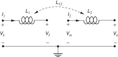
Figure B.7 Equivalent circuit for coupled inductances.
A more appropriate statement for mutual inductance can be used for the mutual inductance input descriptions. Due to the symmetry ![]() , a better statement for the mutual coupling is
, a better statement for the mutual coupling is
KL12 Lp11 Lp22 0.0005uH TD=0.132nsWe also included a time delay example in this statement. This would be the delay for mutual inductances. The stamp for this case is given in Table B.10. The structure of the stamp is the same for the time domain.
Table B.10 Matrix element stamps for inductances and mutual inductances.
| Row/column | RHS | ||||||
| 1 | |||||||
| 1 | |||||||
| Aux | 1 | ||||||
| Aux | 1 |
For the time domain, we replace ![]() with the appropriate numerical integration method in the auxiliary equations.
with the appropriate numerical integration method in the auxiliary equations.
B.1.8 Ideal Transformer Model
The ideal transformer is an important element in circuit theory that finds use for circuit synthesis and other applications. Importantly, this circuit element does not contribute to the states of the MNA descriptor system and it is also lossless. We can write the conventional circuit equations in terms of the ratio of the primary to secondary voltage ratio ![]() with the current ratio of
with the current ratio of ![]() such that power is conserved (Fig. B.8).
such that power is conserved (Fig. B.8).

Figure B.8 Equivalent circuit for ideal transformer with two windings.
The stamp for the ideal two winding transformer is given in Table B.11.
Table B.11 Matrix element stamps for two winding ideal transformer.
| Row/column | RHS | ||||||
| 1 | 0 | ||||||
| 0 | |||||||
| 1 | 0 | ||||||
| 0 | |||||||
| Aux | 0 | 0 | 0 | 0 | 1 | 0 | |
| Aux | 1 | 0 | 0 | 0 |
The ideal transformer stamp for multiple windings is a straightforward extension of the two winding model given here.
B.2 Controlled Source Stamps
Controlled sources are required for a large class of circuit solutions. For PEEC models, current controlled current sources (CCCSs) are used as well as voltage controlled voltage sources (VCVSs). We consider the four combinations between current and voltage sources in the following section.
B.2.1 Current Controlled Voltage Source (CCVS)
The first controlled source stamp we consider is the current controlled voltage source (CCVS). The equation for the voltage is ![]() , where
, where ![]() represents the individual name assigned to the
represents the individual name assigned to the ![]() factor (Fig. B.9).
factor (Fig. B.9).
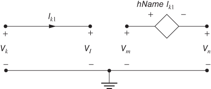
Figure B.9 Equivalent circuit for current controlled voltage source.
Table B.12 Matrix stamp for current controlled voltage source.
| Row/column | RHS | ||||||
| 1 | 0 | ||||||
| 0 | |||||||
| 1 | 0 | ||||||
| 0 | |||||||
| Aux | 1 | 0 | |||||
| Aux | 1 | 0 |
As can be observed, the stamp is given for the case where the current is measured between nodes ![]() and
and ![]() is for the case of a short current measuring connection. The stamp can be simplified if we use a branch current as the measuring element. This part is clearly borrowed from the current measuring in the short stamp in Table B.12.
is for the case of a short current measuring connection. The stamp can be simplified if we use a branch current as the measuring element. This part is clearly borrowed from the current measuring in the short stamp in Table B.12.
B.2.2 Voltage Controlled Voltage Source (VCVS)
Next, we consider the matrix stamp for a VCVS. The auxiliary equation for this case is ![]() . This leads to the matrix stamp of Table B.13 (Fig. B.10).
. This leads to the matrix stamp of Table B.13 (Fig. B.10).

Figure B.10 Equivalent circuit for voltage controlled voltage source.
Table B.13 Matrix stamp for voltage controlled voltage source.
| Row/column | RHS | |||||
| 1 | ||||||
| Aux | 1 |
B.2.3 Current Controlled Current Source (CCCS)
Next, we consider the matrix stamp for a CCCS (Table B.14). The current ![]() . Here,
. Here, ![]() is the current of the source from node
is the current of the source from node ![]() to node
to node ![]() (Fig. B.11).
(Fig. B.11).
Table B.14 Matrix stamp for current controlled current source.
| Row/column | RHS | |||||
| 1 | ||||||
| Aux | 1 |

Figure B.11 Equivalent circuit for current controlled current source.
B.2.4 Voltage Controlled Current Source (VCCS)
The matrix stamp for a voltage controlled current source (VCCS) is used to represent some devices (Fig. B.12, Table B.15). The voltage controlled current is given by ![]() . These stamps, together with Chapter 2, should yield a good understanding on how to form the appropriate circuit equations.
. These stamps, together with Chapter 2, should yield a good understanding on how to form the appropriate circuit equations.

Figure B.12 Equivalent circuit for voltage controlled current sources.
Table B.15 Matrix stamp for VCCS.
| Row/column | RHS | ||||
References
- 1. C. Ho, A. Ruehli, and P. Brennan. The modified nodal approach to network analysis. IEEE Transactions on Circuits and Systems, 22(6):504–509, June 1975.
- 2. J. Vlach and K. Singhal. Computer Methods for Circuit Simulation. Van Nostrand Reinhold Company, New York, 1983.
- 3. A. Ruehli Ed. Circuit Analysis, Simulation and Design, Part 1. Elsevier Science Publishers B.V., North-Holland, 1986.
- 4. L. Pillegi, R. Rohrer, and C. Visweswariah. Electronic Circuits and System Simulation Methods. McGraw-Hill Book Company, New York, 1995.
- 5. F. N. Najm. Circuit Simulation. John Wiley and Sons, Inc., New York, 2010.
- 6. L. W. Nagel. SPICE: a computer program to simulate semiconductor circuits. Electronics Research Laboratory Report, ERL M520, University of California, Berkeley, CA, May 1975.