Cost Considerations for Three-Dimensional Integration*
Abstract
Cost issues for vertical integration are discussed in this chapter. The diverse steps introduced in each of the manufacturing processes for through silicon vias (TSVs) result in different cost requirements. These steps include, for example, TSV etching, lithography, liner processing, barrier and copper (Cu) seed processing, metal plating, surface polishing, and backside processing. Models that capture these cost implications are provided. Other relevant aspects, such as the area of the active die and prebond test coverage, are included in these models. Cost models for interposer-based (2.5-D) systems are also discussed, including redistribution layers, metal–insulator–metal capacitors, microbumps and Cu pillars. In addition, a comparison between the manufacturing cost of 2.5-D and three-dimensional systems is provided.
Keywords
TSV cost modeling; interposer cost modeling; TSV processing steps; TSV yield; interposer yield
Adopting a new technology, in addition to the advantages of system performance, power, and reliability, should also provide benefits in terms of the cost to process each unit. This improvement has occurred with semiconductor manufacturing and scaling of device feature size with each new technology generation. The manufacturing cost per transistor has dropped with device scaling while the transistor operates at higher speeds and consumes less power.
For three-dimensional (3-D) integration technology [49,69] to be widely adopted, the processing cost of the 3-D features and the effect of vertical die stacking on the overall financial cost of a system should be considered in comparison to the benefits in system functionality. These costs are discussed in this chapter. The cost for processing different TSV structures is discussed in Section 8.1. The build-up options for a passive Si interposer substrate, the main component for 2.5-D integration, are considered in Section 8.2. A comparison between the processing costs of 2.5-D and 3-D integration is discussed in Section 8.3. The primary topics of this chapter are summarized in Section 8.4.
8.1 Through Silicon Via Processing Options
The through silicon via (TSV) [312] is the fundamental technology that enables vertical stacking of functional dice. Depending upon the processing stage of the TSVs within the overall process flow, this technology can be characterized as either TSV middle or TSV last, as discussed in Chapter 3, Manufacturing Technologies for Three-Dimensional Integrated Circuits. TSV middle is processed in a wafer after the active devices have been manufactured and prior to fabrication of the on-chip interconnect metal layers. The connection to the bottom side of the TSV is achieved by thinning the wafer and revealing the TSV from the backside. Alternatively, TSV last is processed after completing the full wafer fabrication flow and backside thinning. In this case, a TSV structure contacts the interconnect layers of a die from the backside of the thinned wafer. A cross-sectional representation of both TSV middle [313] and TSV last [314] is shown in Fig. 8.1.

In this section, different TSV options are compared in terms of processing complexity and cost. A 3-D cost model developed at IMEC is applied to evaluate the wafer-level processing cost of different TSV integration approaches [315]. The cost of the tools, infrastructure, personnel, equipment maintenance, and materials is considered in the analysis of each process flow. Furthermore, different TSV geometries are considered to evaluate trends in TSV processing cost with decreasing TSV dimensions.
An overview of the processing steps in the TSV middle and TSV last flows, together with the different TSV geometries, is presented in Section 8.1.1. The cost of each processing step in the different TSV flows is evaluated in Section 8.1.2 for TSVs of different geometries and aspect ratios. The overall cost of the different TSV processing flows is compared in Section 8.1.3, and scaling trends of TSV dimensions are also presented.
8.1.1 TSV Flows and Geometries
The processing flows considered for TSV middle [313] and TSV last [314] are illustrated in Fig. 8.2. A number of similar processing steps are indicated in each flow: lithography, TSV etch, oxide liner deposition, barrier and seed deposition, copper (Cu) plating, and chemical mechanical planarization (CMP). Thinning the wafer from the backside is also included in both flows, although in the TSV last flow thinning is completed before processing the TSV, while in the TSV middle flow, thinning of the wafer is processed after TSV processing. Differences between the flows are: (1) opening of the in-via liner after deposition (liner etch) in the TSV last flow, and (2) opening of the TSV liner after thinning the wafer in the TSV middle flow. These different processing steps are illustrated in the rows shown in Fig. 8.2.

Different TSV geometries are evaluated for each TSV flow. The size of the TSV is given by the TSV diameter and depth using the notation TSV diameter×TSV depth, with each dimension in micrometers. In the case of TSV middle, sizes of 10×100, 5×50, 3×50, and 2×40 µm2 TSVs are considered. In the case of TSV last, dimensions of 10×100, 10×50, 5×50, and 2×20 µm2 TSVs are evaluated, as summarized in Table 8.1. Processing of a TSV middle 5 µm ×50 µm is considered as the reference flow (process-of-reference—POR) for all of the TSV geometries. The processing costs are therefore normalized to the cost of the 5×50 TSV middle flow [313].

8.1.2 Cost Comparison of Through Silicon Via Processing Steps
In this section, the effects of TSV geometry and process flow on the cost and complexity of each process step are explored. The requirement for different processing conditions depending upon the TSV dimensions is indicated for each step, and the effect on subsequent steps (such as CMP) is also reviewed.
8.1.2.1 Through silicon via lithography
A lithography step is executed to develop the TSV structure. The primary difference between the TSV middle and TSV last flow is that the lithography for the TSV middle is processed at a front-end-of-line fabrication compatible tool. In the case of TSV last, an outsourced semiconductor assembly and test (OSAT) fabrication compatible tool is used which is considered to be low cost. This difference results in a TSV lithographic cost which is approximately 30% more expensive for the TSV middle flow as compared to the TSV last flow. The same tool throughput and material costs for photoresist are considered for both flows. Furthermore, no difference in lithography cost is observed due to the different TSV dimensions. A comparison of the lithography processing cost for the different TSV flows and dimensions is shown in Fig. 8.3. The processing cost is normalized to the cost of the POR flow, the 5×50 TSV middle.

8.1.2.2 Through silicon via silicon etch
A deep silicon etch process is considered as the first step after lithography in producing TSV structures. The processing time for TSV etch depends upon the TSV depth and aspect ratio. TSVs that are deeper and narrower require additional etch cycles. The effect of the TSV geometry on the cost of a TSV etch step is illustrated in Fig. 8.4. In addition, the effect of the etching time on cost is illustrated in terms of the processing throughput, expressed as wafers per hour (WPH). As shown in Fig. 8.4, shorter TSVs exhibit a faster etching time (for example, the 5×50 vs. the 10×100 TSV process). In addition, those TSVs with a more aggressive aspect ratio require more time to etch (the 3×50 TSV middle as compared to 5×50 TSV middle, or the 5×50 TSV last as compared to 10×50 TSV last). The cost of the various gases used during the etching process is treated as a material cost. Furthermore, all of the etch processing costs are normalized to the cost of etching a POR structure, a 5×50 µm2 TSV middle structure.

8.1.2.3 Through silicon via liner processing
Following the opening of the TSV hole, an insulating oxide liner layer is deposited. In the case of TSV middle, different liner deposition approaches are applied, depending upon the aspect ratio of the TSV. In the case of aspect ratios up to 1:10, a tetraethylorthosilicate (TEOS) oxide is deposited with different thicknesses (800 nm for a 10×100 TSV and 400 nm for a 5×50 TSV). However, as the TSV aspect ratio increases (for 3×50 and 2×40 TSVs), a more conformal liner layer is required with higher uniformity in the liner thickness along the TSV [317]. A plasma enhanced atomic layer deposition (PEALD) oxide deposition approach is therefore preferred to achieve a liner thickness of 100 nm, capped with a 30 nm silicon nitride (SiN) layer deposited at the wafer field. The various liner processing options for the different TSV geometries are illustrated in Fig. 8.5.

Additionally, in the case of the TSV middle flow, the deposited oxide liner layer on the field is eventually removed by CMP. The effect of CMP liner polishing on the overall processing cost is illustrated in Fig. 8.5, where the cost of the liner CMP process and the CMP slurry required to polish the liner is considered for the TSV middle flow. The cost of the CMP depends upon the thickness of the deposited liner.
In the case of a TSV last flow, the liner needs to be opened (etched) at the bottom of the via prior to further processing; therefore, a highly conformal layer is required. For this reason, PEALD oxide deposition is used for all TSV geometries processed with the TSV last approach. Furthermore, the liner at the top of the TSV should be protected when opening the TSV liner at the bottom of the via. Liner protection is achieved by depositing a capping layer of 450 nm SiN on top of the deposited liner. Finally, in the case of TSV last, it is not necessary to polish the liner. No additional CMP cost is therefore incurred.
8.1.2.4 Through silicon via liner opening for through silicon via last flow
In the case of the TSV last process flow, the oxide liner layer at the bottom of the TSV is opened after deposition to provide a conductive path to the metal layers of the bottom device plane. This step is one of the differentiating steps between the TSV middle and TSV last flows.
A comparison of the processing cost of the liner etch step for different TSV last geometries is illustrated in Fig. 8.6. Note that processing times vary depending on the size of the TSV, resulting in variations in process throughput. Longer processing times (resulting in smaller tool throughput) are required for the narrower TSV diameters. In this case, a 5×50 TSV last process is used as a reference. All of the processing cost is normalized to the cost of the liner opening of a 5×50 TSV last structure.

8.1.2.5 Through silicon via barrier and Cu seed processing
The first steps towards metallization of a TSV structure are the deposition of a barrier layer to prevent Cu diffusion, followed by a deposition of a Cu seed layer to allow the Cu filling of the TSV through electroplating. Two main requirements for these layers are continuity and uniformity throughout the TSV structure. With highly scaled TSV geometries, achieving these requirements is a challenge; different deposition options are therefore considered for different TSV sizes [316,317].
In the case of a TSV middle flow with an aspect ratio of 1:10 (i.e., 10×100 and 5×50), a physical vapor deposition (PVD) tantalum (Ta) barrier layer followed by a PVD Cu seed layer is applied [313]. Different layer thicknesses are required to achieve continuity for the different TSV sizes: For a 10×100 TSV, a Ta layer of 180 nm followed by a 1,500 nm Cu seed is used. In the case of a 5×50 TSV, layers of 130 nm Ta and 800 nm Cu are used, as illustrated in Fig. 8.7.

With further scaling of the TSV diameter and increasing TSV aspect ratios, however, the PVD deposition process reaches a limit and alternative deposition technologies such as atomic layer deposition (ALD) processing are considered. As shown in Fig. 8.7, ALD deposition of 12 nm titanium nitride (TiN) has been demonstrated as a successful barrier layer for a 3×50 TSV middle structure [316]. PVD Cu deposition with a thickness of 1,500 nm is an option for the seed layer to achieve continuity through the entire TSV, albeit with variations in thickness. Another option for a conformal seed is the combination of 5 nm ALD ruthenium (Ru) with 30 nm electro-less (ELD) Cu deposition [320]. Finally, a third metallization option combines the deposition of a 17 nm tungsten nitride (WN) barrier layer followed by ELD of nickel boron (NiB) that acts as the seed for the Cu plating [317]. As shown in Fig. 8.7, these last two options are scalable and can also be applied to 2×40 TSV middle structures.
The barrier and seed layers are removed by CMP after the TSV process flow. The cost of the CMP process depends upon the thickness of the deposited layers. Therefore, as shown in Fig. 8.7, the thin layers deposited by the ALD and ELD methods offer an advantage from a cost perspective when also considering the processing cost of the CMP.
In the case of a TSV last flow, the TSV geometries considered here allow the use of PVD processes for barrier and seed deposition. Depending upon the TSV geometry, different deposition thicknesses are required to achieve continuous coverage within the TSV, as shown in Fig. 8.8. For smaller diameter TSVs (i.e., 2×20), a thicker seed layer is deposited. The cost of the CMP process to remove the barrier seed layers also depends upon the thickness of the deposited material, as shown in Fig. 8.8.

8.1.2.6 Through silicon via Cu plating and effect on chemical mechanical planarization
Filling the TSV structure with Cu is achieved with a bottom-up electroplating approach that produces void free TSV plating [318]. As shown in Fig. 8.9, the plating time and material cost for TSV filling depends upon the depth and diameter of the TSV structure.

TSV plating overburdens the Cu plated on top of the entire wafer area which is removed by CMP. The Cu CMP process has two stages: (1) a bulk Cu polish that is relatively fast and removes most of the plated Cu, and (2) a fine Cu polish that is slower and clears the remaining Cu traces from the wafer surface (including the Cu seed layer). The fine Cu polish step removes the final layer of Cu (approximately 250 nm) from the top of the wafer.
To estimate the effect of the Cu overburden on CMP cost, the combined effect of the two polishing steps is considered. Different initial Cu overburden thicknesses are considered, from 250 nm up to 3,000 nm, as shown in Fig. 8.10. Note in Fig. 8.10 that for a Cu overburden thickness up to 2,000 nm, the fine Cu polish step dominates the processing time, material cost, and throughput of the CMP process. The CMP cost therefore exhibits low sensitivity to the thickness of the Cu overburden. When the total Cu overburden thickness exceeds 2,000 nm, the time to polish the bulk Cu is dominant and the throughput of the CMP depends upon the overall Cu overburden thickness.

8.1.2.7 Through silicon via chemical mechanical planarization processing
Polishing the deposited layers during TSV formation electrically isolates the TSVs and allows the processing of additional layers, such as the BEOL stack (in the case of TSV middle) or redistribution layers and/or microbumps (in the case of TSV last). In the previous sections, the relative cost to remove each deposited layer by CMP has been described. It is shown that the cost of CMP depends upon the material being removed and the material thickness. Different CMP slurries are required depending on the material used, which can greatly affect the overall cost.
To compare the polishing cost of different materials used in TSV processing, the same thickness of 100 nm is assumed for all materials. In this case, one of the parameters that determines the CMP cost is the polishing time, which depends solely on the material. The polishing time determines the throughput of the CMP equipment for each material. Another parameter is the cost of the slurry, since the selection of slurry depends on the material being polished. The cost of the slurry also depends on the polishing time; however, for materials that require the same polishing time, the type of slurry is the cost differentiator. In Fig. 8.11, the materials used for the different TSV processing options are depicted with respect to CMP time and slurry cost (assuming 100 nm of material thickness). For each material, both the polishing time and the slurry cost are normalized to polish a bulk 100 nm thick Cu layer.

The different materials are grouped in Fig. 8.11 based on the function within the TSV structure. For the plated Cu and Cu seed (illustrated in Fig. 8.11 with dots), polishing the fine Cu layer requires more time than bulk Cu (for the same 100 nm thickness) and the slurry cost scales accordingly. In the case where the fine Cu polishing is above a NiB or Ru seed layer, a different, more expensive slurry is used, requiring the same approximate processing time.
In the case of non-Cu seed layers such as NiB or Ru (illustrated as diamonds in Fig. 8.11), the cost for Ru polishing can be quite high. The actual Ru thickness is, however, only 5 nm (rather than 100 nm), allowing the use of Ru as a viable option for TSV processing.
For barrier materials such as PVD Ta, ALD TiN, and ALD WN (illustrated in Fig. 8.11 as stars), the polishing rate for the Ta layer is faster than for the ALD layers. However, in an actual TSV structure, the thickness of the ALD layers is an order of magnitude thinner than the thickness of the Ta layer (as previously shown in Fig. 8.7), which can significantly affect the cost of the barrier CMP.
In the case of TSV oxide liner materials such as TEOS oxide, PEALD oxide, and SiN capping (illustrated as triangles in Fig. 8.11), the polishing cost of the TEOS and PEALD oxides is comparable. In a TSV structure, however, the thickness of the PEALD layer is approximately half of the thickness of the TEOS layer, which greatly lowers the liner polishing cost, as shown in Fig. 8.5. Polishing the SiN capping layer is more expensive than the oxide layers. However, in the TSV last flow, polishing the SiN capping layer is an option, eliminating the CMP step.
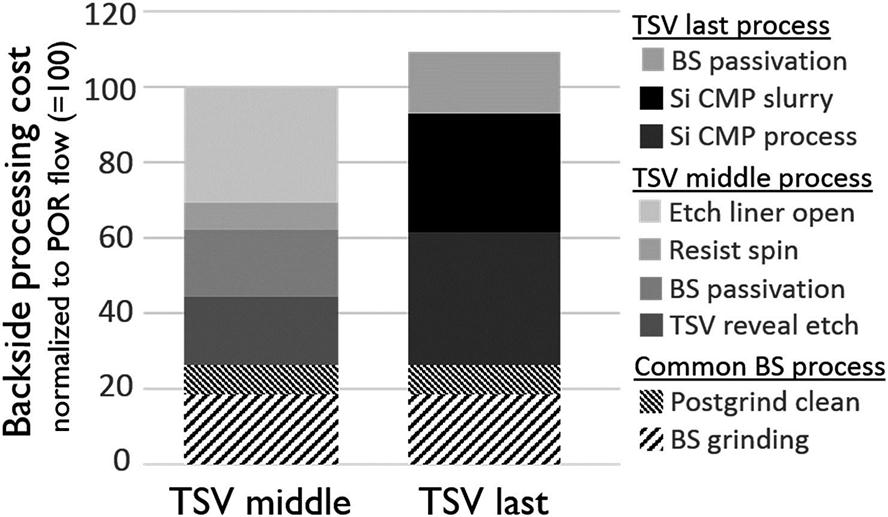
8.1.2.8 Backside processing
Processing a TSV structure requires the wafer to be thinned to a thickness comparable to the TSV depth. Thinning of the wafer is accomplished from the backside by a grind and recess etch step [319]. Depending upon the type of TSV process (TSV middle or TSV last), different processing steps are performed at the backside, as illustrated in Fig. 8.2. These steps and a comparison of the corresponding processing costs are presented in this subsection.
In both the TSV middle and TSV last flows, the wafers are initially ground from the backside followed by cleaning steps. In the case of the TSV middle, recess etching of the Si is completed following a cleaning step to reveal the TSV, with the oxide liner layer fully enclosing the Cu TSV core. As a next step, backside passivation is deposited, followed by a layer of photoresist to protect the passivation layer. During the next step, the protective resist and oxide liner are etched to reveal the Cu core within the TSV. Stripping the remaining photoresist from the backside of the wafer is the final etching step.
In the case of TSV last processes, polishing the Si is completed following the backside grinding and cleaning steps. The polishing is accomplished via CMP to remove any damage caused by the grinding process, and to provide a pristine surface for the subsequent TSV last processing steps. For the TSV last process, a 7 µm thick Si layer is removed by CMP. After the CMP step, a passivation layer is applied at the backside and the TSV last flow is initiated, as illustrated in Fig. 8.2.
The backside processing for the TSV middle and TSV last flows are illustrated in Fig. 8.12. No practical difference exists in the common backside processing steps required for different TSV geometries with either the TSV middle or TSV last flows. Comparing the overall cost of the processing steps for the TSV middle flow with the corresponding cost in the TSV last flow, the TSV last backside processing costs are approximately 10% higher due to the Si CMP.
8.1.3 Comparison of Through Silicon Via Processing Cost
Following the cost benchmarking of the different processing steps in the TSV middle and TSV last integration flows, the cost of the overall fabrication process is compared for different TSV geometries. This comparison is illustrated in Fig. 8.13.

Following the cost benchmark depicted in Fig. 8.13, fabrication of particular TSV geometries is described to evaluate the effect of the individual processing steps. The process flows for these TSV geometries are compared in the following subsections.
8.1.3.1 Processing of the 5×50 through silicon via geometry
The overall processing cost for the 5 µm × 50 µm and 10 m × 100 µm TSV flows is shown in Fig. 8.14 to emphasize the difference between the TSV middle, and TSV last flows for a particular TSV dimension. In the case of the 5×50 TSV middle flow, the oxide liner is removed by CMP, which increases the cost of CMP processing. However, in the case of a TSV last process, the additional cost for the PEALD liner, etching the TSV liner within the via, and the backside CMP results in higher processing cost by up to 10% for the 5 µm × 50 µm TSV flow.

8.1.3.2 Processing of the 10×100 through silicon via geometry
In the case of the 10×100 TSV last geometry, skipping the CMP of the oxide liner reduces the overall processing cost about 9% as compared to the 10×100 TSV middle flow, as shown in Fig. 8.14. Removal of the thick (800 nm) TEOS oxide liner layer is the reason for the lower CMP cost between the two TSV flows.
8.1.3.3 Scaling through silicon via geometries
For the TSV middle flows shown in Fig. 8.15, scaling the TSV size is possible while maintaining reasonable processing costs. This situation is achieved by replacing the thicker PVD deposited layers used in the larger TSV geometries with thinner ALD layers for the scaled TSVs. Although the processing cost of the ALD layers is higher, the cost for CMP polishing of these thinner layers is lower. This trade-off controls the processing cost as the size of a TSV middle is scaled from 5 × 50 to 3 × 50 and 2 × 40 TSV sizes. Scaling the TSV diameter enables scaling of the TSV pitch as well, therefore higher TSV density can be achieved without increase in cost.

8.2 Interposer-Based Systems Integration
An alternative to multiple die vertical stacking is 2.5-D integration of dice on an interposer substrate [321]. In this way, fine pitch interconnections are provided between active dice. This approach addresses the manufacturability and thermal behavior of multi-die 3-D stacks [322]. An additional benefit of 2.5-D integration is that this technology does not require TSVs to be processed within the active dice (the TSVs are only processed in the interposer substrate), removing any uncertainty in the component supply chain, an issue greatly affecting the widespread adoption of 3-D technology.
An example of a system integrated on an interposer substrate is illustrated in Fig. 8.16. High-density interconnections on the interposer substrate provide high bandwidth data transfer between memory and the central processing unit. The interposer contains TSVs that provide connectivity between the system components and the outside world. Additional components provide system level I/O and sensor based functionality integrated onto the interposer substrate and in close proximity to the processing unit. Placing all of the components in close proximity benefits system performance and functionality while reducing power dissipation and overall size.

An interposer for interdie interconnections offers the advantage that no TSVs are required within the functional dice, as compared to vertical stacking of dice (i.e., 3-D integration). Only minor modifications to existing components are therefore necessary [323]. Furthermore, flexible system reconfiguration is enabled since a new component can be added, updated, or replaced by only redesigning the interposer substrate. Partitioning a system into different integrated circuits and selectively scaling different components to optimize the overall system performance and cost is also possible. In addition, the use of an interposer thermally isolates the high power system components.
All of these advantages of an interposer for system integration require manufacturing an additional substrate layer; the additional cost of the interposer on the overall system cost should therefore be considered. Different options for manufacturing an interposer substrate are described in this section and compared in terms of processing cost. Minimum requirements for an interposer substrate include interconnections among the stacked component dice and connections to the outside world through TSVs. In addition, system level power delivery planes are possible with or without incorporating decoupling capacitors within the power distribution network.
The effect of different interposer manufacturing options on system cost is evaluated using the 3-D cost model developed at IMEC [315]. In Section 8.2.1, the processing cost of the various features of an interposer substrate is described. The cost of different interposer configurations is discussed in Section 8.2.2.
8.2.1 Cost of Interposer Manufacturing Features
In this section, the cost of processing different features on an interposer substrate is presented. These features include TSVs, die-to-die interconnect, power and ground planes, metal–insulator–metal (MIM) capacitors, microbumps for functional die stacking, and backside Cu pillars to connect the interposer to the package substrate. Combinations of these structures provide options for an interposer substrate to satisfy different application requirements. A comparison of the relative processing costs per wafer of these components is illustrated in Fig. 8.17.

8.2.1.1 Cost of through silicon via processing
TSVs are fabricated within the interposer substrate to provide connectivity between the stacked functional dice and the package substrate. For the TSVs within an interposer substrate, no strict area constraints exist, and therefore, extreme TSV scaling is not necessary. The interposer thickness, however, is important. To enhance mechanical support, reducing die warpage and improving the ability to handle thin dice necessitate the silicon substrate to not be extremely thin. An interposer composed of TSVs with 100 µm depth and 10 µm diameter (10×100 TSV middle) is therefore considered. The processing cost of the 10×100 TSV middle is the reference to compare the cost of the other interposer components, as shown in Fig. 8.17. A benchmark of the TSV processing cost for different TSV geometries and flows is also illustrated in Fig. 8.13.
8.2.1.2 Cost of die-to-die interconnect processing
The interconnect metal layers providing connectivity among the stacked dice are processed on the interposer substrate. To support high bandwidth communication among the functional dice, low resistance interconnect is required. Thick copper interconnect lines and dielectric thicknesses of up to 2 µm are therefore considered [326]. These lines are manufactured by a dual damascene process to achieve higher line density and enhanced reliability as compared to alternative interconnect processes using semi-additive electrochemical plating [315].
The processing cost per wafer of the dual damascene interconnect lines is illustrated in Fig. 8.17, normalized to the cost of processing a 10×100 TSV middle flow. Note that the dual damascene process forms both the metal lines and the metal vias to the underlying metal interconnect layer. For the lowest metal layer on top of the TSVs, no vias (or substrate contacts) are necessary. This metal layer is in direct contact with the TSVs and can be processed with a single damascene process. The cost of a single damascene line is also shown in Fig. 8.17.
8.2.1.3 Cost of processing metal planes and metal–insulator–metal capacitors
In addition to the metal lines connecting the functional stacked dice, the metal planes that distribute system level power and ground can also be integrated onto an interposer substrate. These power planes use a single Cu damascene process with a metal thickness of 1 µm [324]. Furthermore, the coexistence of both power and ground planes on the same interposer substrate enables the fabrication of a MIM capacitor that can function as a decoupling capacitor within the power distribution network [325]. The MIM capacitor is formed by deposition of a stack of TaN/insulator/TaN layers on top of a planarized metal layer. A second metal plane on top of the stack is the top capacitor terminal, as discussed in [321].
Processing thick metal planes can induce significant stress on the interposer substrate, introducing the risk of die warpage. Leveraging the interaction among the MIM capacitors, thick interconnect lines, and dielectric layers can mitigate the induced stresses during manufacturing of the interposer while restraining die warpage [324].
The cost of processing a single damascene metal plane and the MIM layer stack is illustrated in Fig. 8.17. The cost of a MIM capacitor, comprised of two metal planes with a dielectric insulator in between, is also shown in Fig. 8.17.
8.2.1.4 Cost of processing microbumps and Cu pillars
Communicating signals and power among the functional stacked dice and interposer substrate is achieved by vertical microbumps. High density interconnects are required for wide I/O applications; therefore, small pitch microbump structures are necessary. Cu–Sn–Cu microbump structures with a 20 µm pitch are described in [326]. Furthermore, the interposer connects the backside to the package substrate where a more relaxed interconnect pitch is possible. These connections use Cu pillars with a 170 µm pitch and up to 50 µm thickness.
The processing cost for the microbump structures and Cu pillar structures is illustrated in Fig. 8.17. The larger dimensions and increased metal volume of the Cu pillars require additional processing time, which increases the process cost per wafer as compared to manufacturing microbumps.
8.2.2 Interposer Build-Up Configurations
Exploiting the interposer features described in Section 8.2.1, different interposer configurations can serve different applications. In these systems, the interposer substrate includes microbumps and thick interconnect lines for signaling among the stacked functional dice. Additionally, TSVs and Cu pillars for signaling and power can be accessed at the backside of the interposer and package substrate.
Different interposer systems exhibit different features. Multiple layers of metal lines in the interposers increase routing complexity. Entire metal planes can be used to distribute system level power or ground. Two power metal planes separated by a dielectric can provide a low impedance power distribution network with decoupling capacitance to reduce power supply noise.
Three examples of different interposer configurations are shown in Fig. 8.18. A substrate with a single thick metal layer on top of a reference power plane is shown in Fig. 8.18A. This interposer can be used for applications with a limited number of lines connecting the functional dice. If additional routing is required, a second thick metal layer can be utilized in place of the metal plane, as illustrated in Fig. 8.18B. Finally, an interposer substrate with a MIM capacitor between the power and ground planes and two layers of thick metal lines is depicted in Fig. 8.18C.

A breakdown of the wafer processing cost for each interposer substrate is shown in Fig. 8.19. The cost of each component is normalized to the wafer processing cost of 10 µm × 100 µm TSV middle flow. Note that replacing a metal plane with a routing metal layer has almost no effect on the processing cost. Adding the functionality of a MIM capacitor, however, increases the processing cost of an interposer with two routing layers by up to 40%, as illustrated in Fig. 8.19.

8.3 Comparison of Processing Cost for 2.5-D and Three-Dimensional Integration
In Sections 8.1 and 8.2, the processing cost for different TSV structures and features of a Si interposer substrate are described. These integration schemes can be used to analyze and compare the cost of different 3-D stacking approaches: (1) die-to-wafer (D2W) stacking, (2) wafer-to-wafer (W2W) stacking, and (3) 2.5-D interposer-based stacking. These stacking approaches are illustrated in Fig. 8.20.

For each 3-D stacking approach, the required processing components and complexity of the 3-D processing flows are reviewed. In addition, process yield and prestack testing of the stacked components are evaluated, and the effect on processing cost is described. Furthermore, the effect of die size on system yield and 3-D integration cost is discussed.
This section is organized as follows: The different stacking schemes and components that enable vertical integration are presented in Section 8.3.1. A comparison of the processing cost of the different components enabling 3-D integration is discussed in Section 8.3.2. The complete 3-D integration flow, together with different options for prestack testing, are compared in Section 8.3.3. The effect of the size of the active dice on the integration cost is reviewed in Section 8.3.4. Further exploration of the impact of prestack testing of the interposer in relation to processing yield and the size of the active dice is discussed in Section 8.3.5.
8.3.1 Components of a Three-Dimensional Stacked System
A 3-D stacked system with three active dice is considered here. All of the dice are assumed to be processed in the same CMOS technology (28 nm bulk CMOS is assumed) and are the same size to enable W2W stacking. The die area, however, can vary to evaluate the effects of die size and number of die per wafer on the processing yield and system cost.
The processing yield of the active dice is determined from the Poisson yield model, Y=e(−AD) [327], where A is the die area and D is the defect density per unit area. The defect density is assumed to be 5% for the particular process technology, while the die area can vary.
It is further assumed that the active dice are tested prior to stacking with a total fault coverage of 95%. Consequently, testing can detect 95% of the faults on a die, where the faulty dice are scrapped; however, there remains a possibility of 5% faulty dice. In the cases of D2W stacking and stacking on an interposer substrate, only those active dice that pass prestack test are selected for stacking. In the case of W2W stacking, the location of each die on a wafer is set; therefore, no prestack test of the active dice is performed. The cost for testing the active dice is considered to be proportional to the die area.
In the case of D2W and W2W stacking, the TSVs are placed between the active dice to enable the vertical interconnections. The stacking interface among the dice uses microbumps. An illustration of the resulting stack of three dice is shown in Fig. 8.21A. The bottom die in the stack uses Cu pillars of 50 µm height to connect to a laminate package substrate (the cost of a package substrate is not considered in this cost comparison). The top die in the stack does not contain TSVs; the top die is stacked face-to-face to the die below it.

In interposer-based systems, the active dice are stacked face-to-face on a silicon interposer substrate using microbumps between layers. The interposer provides the multiple interconnections among the active dice. Furthermore, the interposer provides backside access to the package substrate using TSVs for the power supply and I/O signals. No TSVs are fabricated within the active dice. An interposer substrate with three stacked dice is shown in Fig. 8.21B.
The interposer substrate die should be sufficiently large to accommodate the three dice stacked on top. It is assumed that the interposer die extends 100 µm around the active die area. As the size of the active dice can vary, the interposer die is resized to fit the stacked dice.
8.3.2 Cost of Three-Dimensional Integration Components
To evaluate the cost of a 3-D system, the processing cost for the components that enable 3-D stacking should be considered in addition to the processing cost per wafer of the active dice. In the case of a 3-D system where the active dice are stacked on top of each other, as illustrated in Fig. 8.21A, the additional cost includes:
1. For die 1: Microbumps on the front side, TSVs (with backside processing and thinning), and Cu pillars at the backside.
2. For die 2: Microbumps on the front and backside and TSVs (with backside processing and thinning).
The TSVs processed within the active dice are considered to be 5×50 TSV middle structures [313], as described in Section 8.1.1.
In the case of an interposer-based system, the microbumps are processed on the face of the active die to interface with the interposer substrate. Furthermore, an additional component is the interposer die itself. Processing all of the features on the interposer dice, as shown in Fig. 8.21B, should therefore be considered:
1. Microbumps on top of the interposer.
2. Interconnect to provide connections among the stacked active die.
3. TSV processing (including temporary wafer bonding and wafer thinning).
4. Cu pillar processing at the backside to connect to the package substrate.
An interposer substrate with two thick metal lines, as illustrated in Fig. 8.18B, is considered in this comparison. The TSVs processed within the interposer die have a diameter of 10 µm and and a height of 100 µm (10×100 TSV middle process), as discussed in Section 8.1.1.
In both vertically stacked and interposer-based systems, the microbumps are assumed to have a 40 µm pitch and a bump diameter of 25 µm [326]. The Cu pillars have a minimum pitch of 170 µm and a diameter of 50 µm.
A comparison of the processing cost per wafer for the components that enable 3-D stacking is shown in Fig. 8.22. The processing steps for temporary wafer bonding, wafer thinning, and die stacking are also included. Notice in Fig. 8.22 that the “die pick and place” step is a die level process, and the wafer-level cost depends upon the number of dice per wafer. In this case, active dice with size of 10 mm×10 mm are assumed, resulting in 568 dice on a 300 mm wafer. Only those dice that pass a prestack test, however, are chosen for stacking. Assuming a 5% per cm2 defect density and prestack testing of the active dice with 95% fault coverage, 541 dice will pass testing. The cost for the “die pick and place” operation therefore assumes 541 die per wafer.

8.3.3 Comparison of Three-Dimensional System Cost
A comparison of the cost of vertically stacked systems with three different 3-D integration approaches is presented in this section. The approaches are: D2W stacking, W2W stacking, and a 2.5-D interposer-based system. The cost comparison considers a system with three active dice, 10 mm×10 mm in size.
For each approach, the cost of the 3-D system is determined by evaluating the cost of the individual processing components. The cost of each active die includes CMOS processing, additional processing for those features that enable 3-D stacking (TSVs, wafer thinning, microbumps), and the cost of prestack testing. Furthermore, yield losses due to imperfect 3-D stacking (the stacking yield is assumed to be 98%) and test fault coverage (assumed at 95%) are also considered. The cost of each stacked component and the cost of the total 3-D system for each stacking approach is depicted in Fig. 8.23.

As shown in Fig. 8.23, in the case of D2W and W2W stacking, the 3-D enabling cost for die 1 and die 2 is greater than the corresponding cost for die 3 since the TSVs are processed within dices 1 and 2. Furthermore, the cost of prestack testing of the active dice is included in the D2W approach. The cost of the D2W stack is the sum of the processing costs of the individual active dice, 1, 2, and 3, and the cost due to compound yield losses. Compound yield losses are due to imperfect yield of the 3-D stacking process (shown in Fig. 8.23 as stacking yield cost) and the nonperfect testing of the active dice, assuming a fault coverage of 95% (shown as die yield cost). These yield losses are due to a small portion of faulty active dice that are misplaced during test and contribute to the cost due to die yield loss.
In the case of W2W stacking, no testing of the active dice is required since the position of the stacked dice is fixed. The processing cost of the individual active dice is therefore lower than the D2W approach. There is, however, an increased cost due to yield loss due to stacking of faulty active dice, as illustrated in Fig. 8.23.
In the case of an interposer-based system, an additional system component needs to be manufactured: the interposer die. The processing yield of the interposer die is assumed to be 99% and the interposer dice are tested with 100% fault coverage. Processing of the interposer die is an additional 3-D enabling cost, as illustrated in Fig. 8.23. Note in Fig. 8.23 that the cost due to stacking yield loss is higher for an interposer-based system. This characteristic is due to the additional stacking operation required to place the interposer die on the package substrate, affecting the overall stacking yield.
8.3.4 Dependence of Three-Dimensional System Cost on Active Die Size
In this section, the effect of the active die size on the cost of a 3-D system is evaluated. Different active die sizes, ranging from 3 mm×3 mm to 15 mm×15 mm, are considered. The same assumptions as in the previous sections are valid regarding component processing, assembly yield, and prestack test fault coverage. Considering a variable active die size, the process cost per die area is determined, including the cost of CMOS processing of the active dice, additional 3-D enabling cost (including the interposer processing cost for the 2.5-D interposer system), and the cost for testing the active dice and interposer. In addition, the cost of the compound yield loss due to 3-D stacking is reported. Summing the cost due to process with the cost due to compound yield loss produces the total cost per die area. The process cost per die area and the total cost per die area are shown in Fig. 8.24 for the three different stacking approaches.

As shown in Fig. 8.24, the stack cost per unit area for all three integration approaches increases with the size of the active dice. This increase in cost is due to the smaller number of dice per wafer and the lower utilization of the total wafer area. Furthermore, with increasing die size, the processing yield of the active dice is less; thereby increasing the process cost of each system.
Considering the D2W stacking approach, the total cost of the 3-D stack per unit area is almost a constant offset higher than the process cost over the entire range of active die area. This constant offset in cost is the effect of prestack testing of the active dice that greatly reduces yield loss due to faulty active dice. The yield losses in this case are due to the nonperfect yield of the 3-D stacking process (98%) and the small fraction of active dice that are misplaced during prestack testing.
In the case of the W2W stacking approach, as shown in Fig. 8.24, the process cost per unit area is lowest. This low cost is due to no prestack test of the active dice. However, when the total cost of the 3-D stack is considered, the effect of the compound yield losses is quite significant. Particularly for large active dice, the cost of the compound yield losses becomes comparable to the process cost of the stacked dice. Alternatively, as shown in Fig. 8.24, for small active die, the overall 3-D stack cost per unit area for the W2W approach is lower than the cost of the same system with D2W stacking.
For a 2.5-D interposer-based system, processing the additional component (interposer die) affects the process cost of the system. In the particular case that the interposer process yield is high (99%) and the interposer die is tested prior to stacking (with 100% fault coverage), as shown in Fig. 8.24, the total cost of the 2.5-D interposer system is an almost constant offset higher than the process cost.
8.3.5 Variation of Interposer Process Yield and Prestack Fault Coverage
Further discussion is presented in this section on the cost of an interposer-based system. The processing yield of an interposer die is varied from 99% per cm2 to 90% and 80% per cm2. Furthermore, the fault coverage of interposer die testing prior to stacking is varied from 100% to 50% and 0% (no testing). Active dice with a size of 10 mm×10 mm are assumed to be stacked on the interposer. The effect of the variable process and test parameters on the cost of a 3-D interposer-based system is illustrated in Fig. 8.25.

As shown in Fig. 8.25, when the processing yield of an interposer is high (99%), the cost of testing the interposer die incrementally adds to the total system cost. It is therefore preferable to not test the interposer and tolerate the small cost due to interposer yield losses. In this case, the loss of the good active dice stacked on the interposer is lower than the cost to test an interposer die with a processing yield of 99% per cm2.
As the interposer processing yield drops to 90% and 80% per cm2, prestack test of the interposer die becomes advantageous. As shown in Fig. 8.25, the cost for testing an interposer is lower than the cost due to losses from nonperfect interposer processing. In these low interposer yield cases, the higher the fault coverage for interposer testing, the lower the cost due to yield loss.
The cost of a 3-D interposer system across a wide parameter space can be described by these experiments. In addition to variations in processing yield and fault coverage, differences in the active die size between 3 mm×3 mm and 15 mm×15 mm are considered. The cost of a 2.5-D interposer-based system per unit area is evaluated for each parameter, as illustrated in Fig. 8.26.

The interposer processing yield per cm2 is varied along different rows in Fig. 8.26 with the corresponding yield noted to the left of each row (respectively, 99%, 90%, and 80% yield per cm2). Similarly, the fault coverage for the interposer dice is varied in different columns. The fault coverage for interposer testing is reported at the top of the corresponding column in Fig. 8.26 (respectively, 100%, 50%, and 0% fault coverage).
As shown in Fig. 8.26, as the processing yield of the interposer decreases, the system cost increases. This increase can vary dramatically if no testing of the interposer die occurs, as shown in Fig. 8.26I. Furthermore, the system cost also increases with increasing size of the active die. The active dice become more expensive, requiring large interposers for system integration. Therefore, particularly in the case of large active dice, stacking these dice on an untested interposer substrate with low processing yield can cause a significant increase in the cost of a 3-D system.
8.4 Summary
• The primary cost contributors in TSV processing are CMP, deep Si etch, and barrier and seed deposition. These processing cost components are valid for different TSV geometries, considering both TSV middle and TSV last process flows.
• The TSV middle flow provides a simpler process without requiring protection and in-via etching of the TSV oxide liner.
• For TSV middle flows, the deposited oxide liner should be removed by CMP. This step can significantly increase the cost of the CMP step, particularly for thick oxide liner layers.
• In the case of TSV last processes, an option exists to not remove the oxide liner deposited on the surface of the wafer, simplifying the TSV CMP step.
• Certain processing steps, such as lithography, can be performed less expensively using OSAT grade tools. However, Si CMP at the wafer backside is required before processing the TSVs.
• The oxide liner needs to be opened within the via. These steps increase the processing complexity of a TSV last process.
• Different TSV geometries, such as the TSV depth and aspect ratio, affect the processing cost for similar fabrication flows.
• The TSV size and pitch can be scaled while maintaining reasonable process cost. This situation is achieved by utilizing ALD deposition and depositing thinner layers.
• The processing cost of ALD deposition may be higher than alternative PVD approaches. Deposition of thinner materials, however, lowers the cost of the CMP.
• Reducing the CMP cost for thinner ALD materials introduces a tradeoff that can be exploited to maintain the processing cost of scaled TSVs.
• Stacking active dice on a silicon interposer produces high-density interdie connections without processing TSVs between the dice.
• The interposer features can include TSVs, die-to-die interconnect, power and ground planes, MIM capacitors, microbumps, and backside Cu pillars.
• Combinations of these structures provide varying options for an interposer substrate that satisfy various requirements at different processing costs.
• Three different stacking approaches are considered to compare processing costs at the system level: D2W stacking, W2W stacking, and 2.5-D integration on Si interposers.
• In the case of a D2W process, prestack testing of the stacked components is critical to eliminate bad dice from stacking, limiting yield losses.
• Prestack test is more important when stacking large dice which are more expensive and exhibit lower process yield. In this case, the D2W approach provides the lowest cost for integrating a multidie 3-D system.
• For W2W stacking of active dice, prestack test of the dice is not necessary, saving testing cost.
• W2W stacking produces the lowest processing cost per stacked system among the three stacking approaches considered in the comparison.
• The effect of compound yield losses on cost is significant in the case of W2W stacking of large stacked dice, where the processing yield is lower, increasing the likelihood of stacking a bad die above a good die.
• Large active dice are more expensive and the cost of the scrapped W2W stacks is also higher.
• W2W stacking can be beneficial for 3-D systems with relatively small dice. In this case, many stacks can be produced with a W2W process.
• Stacking of small dice increases the probability of good stacks, and the total stack cost (including compound yield losses) is lower.
• In the case of an interposer-based 2.5-D system, the interposer substrate adds to the overall system cost.
• If the yield for interposer processing is high, the additional processing cost of the interposer makes a 2.5-D system more expensive than 3-D stacks of active dice.
• In the case of large interposer substrates, high processing yield and/or good fault coverage of the interposer make 2.5-D integration a viable solution.
• If the interposer process yield is high, prestack testing of the interposer die may increase overall system cost.
• This cost comparison recognizes the multiple benefits provided by interposer-based 2.5-D system integration such as improved thermal characteristics, limited processing of the active dice (no TSVs), flexibility in system components, and simplifying the supply chain.