
Chapter 40
Design for Production
Really, every chapter in this book has been about design for production. As was implied in the introduction, the ability that marks out a professional designer is the ability to design products or systems that work under all relevant circumstances and which can be manufactured easily.
The sales and marketing engineer addresses the questions, “Can I sell this product?” and, “How much can I sell this product for?” This book hasn’t touched on these issues, important though they are to designers; it has assumed that you have a good relationship with your marketing department and that your marketing colleagues are good at their job. But you as designer also have to address another set of questions, which are:
• Can the purchasing department source the components quickly and cheaply?
• Can the production department make the product quickly and cheaply?
• Can the test department test it easily?
• Can the installation engineers or the customer install it successfully?
It is as well to bear all these questions in mind when you are designing a product, or even part of one. Your company’s financial health, and consequently your and others’ job security, ultimately depends on it. A good way to monitor these factors is to follow a checklist.
40.1 Checklist
40.1.1 Sourcing
• Have you involved purchasing staff as the design progressed?
• Are the parts available from several vendors or manufacturers wherever possible? Have you made extensive use of industry standard devices?
• Where you have specified alternate sources, have you made sure that they are all compatible with the design?
• Have you made use of components that are already in use on other products?
• Have you specified close-tolerance components only where absolutely necessary?
• Where sole-sourced parts have to be used, do you have assurances from the vendor on price and lead time? How reliable are they? Have you checked that there is no warning, “not recommended for new designs” (implying limited availability), on each part?
• Does your company have a policy of vetting vendors for quality control? If so, have you added new vendors with this product, and will they need to be vetted?
40.1.2 Production
• Have you involved production staff as the design progressed?
• Are you sure that the mechanical and electrical design will work with all mechanical and electrical tolerances?
• Does the mechanical design allow the component parts to be fitted together easily?
• Are components, especially polarized ones, all oriented in the same direction on the PCB for ease of inspection and insertion?
• Are discrete components, notably resistors, capacitors and transistors, specified to use identical pitch spacings and footprints as far as possible?
• Have you minimized wiring looms to front or rear panels and between PCBs, and used mass-termination connections (e.g., IDC) wherever possible?
• Have you modularized the design as far as possible to make maximum use of multiple identical units?
• Is the soldering and assembly process (wave, infrared, auto-insert, pick and place, etc.) that you have specified compatible with the manufacturing capability? Will the placement machines cope with all the surface mount components you have used?
• If the production calls for any special assembly procedures (e.g., potting or conformal coating), or if any components require special handling or assembly (MOSFETs, LEDs, batteries, relays etc.) are the production and stores staff fully conversant with these procedures and able to implement them? Have you minimized the need for such special procedures?
• Do all PCBs have adequate solder mask, track and hole dimensions, clearances, and silk screen legend for the soldering and assembly process? Are you sure that the test and assembly personnel are conversant with the legend symbols?
40.1.3 Testing and Calibration
• Have you involved test staff as the design progressed?
• Are all adjustment and test points clearly marked and easily accessible?
• Have you used easily set parts such as DIL switches or linking connectors in preference to solder-in wire links?
• Does the circuit design allow for the selection of test signals, test subdivision and stimulus/response testing (including boundary scan) where necessary?
• If you are specifying automatic testing with ATE, does the pc layout allow adequate access and tooling holes for bed-of-nails probing? Have you confirmed the validity of the ATE program and the functional test fixture?
• Have you written and validated a test software suite for microprocessor-based products?
40.1.4 Installation
• Does the design have adequate EMC?
• Are the installation instructions or user handbook clear, correct and easy to follow?
• Do the installation requirements match the conditions which will obtain on installation? For example, is the environmental range adequate, the power supply appropriate, the housing sufficient, etc.?
40.2 The Dangers of ESD
There is one particular danger to electronic components and assemblies that is present in both the design lab and the production environment. This is damage from electrostatic discharge (ESD). This can cause complete component failure, or worse, performance degradation that is difficult or impossible to detect. It can also cause transient malfunction in operating systems.
40.2.1 Generation of ESD
When two nonconductive materials are rubbed together, electrons from one material are transferred to the other. This results in the accumulation of triboelectric charge on the surface of the material. The amount of the charge caused by movement of the materials is a function of the separation of the materials in the triboelectric series, an example of which is shown in Table 40.1. Additional factors are the closeness of contact, rate of separation and humidity.
Table 40.1 The triboelectric series

If this charge is built up on the human body, as a result of natural movements, it can then be discharged through a terminal of an electronic component. This will damage the component at quite low thresholds, easily less than 1 kV, depending on the device. Of the several contributory factors, low humidity is the most severe; if relative humidity is higher than 65% (which is frequent in maritime climates such as the UK’s) then little damage is likely. Lower than 20%, as is common in continental climates such as the United States, is much more hazardous.
Gate-oxide breakdown of MOS or CMOS components is the most frequent, though not the only, failure mode. Static-damaged devices may show complete failure, intermittent failure or degradation of performance. They may fail after one very high voltage discharge, or because of the cumulative effect of several discharges of lower potential.
40.2.2 Static Protection
To protect against ESD damage, you need to prevent static buildup and to dissipate or neutralize existing charges. At the same time, operators (including yourself and your design colleagues) need to be aware of the potential hazard. The methods used to do this are:
• package sensitive devices or assemblies in conductive containers; keep them in these until use and ensure they are clearly marked;
• use conductive mats on the floor and workbench where sensitive devices are assembled, bonded to ground via a 1 MΩ resistor;
• remove nonconductive items such as polystyrene cups, synthetic garments, wrapping film, etc. from the work area;
• ground the assembly operator through a wrist strap, in series with a 1 MΩ resistor for electric shock protection;
• use ionized air to dissipate charge from nonconductors, or maintain a high relative humidity;
• create and maintain a static-safe work area where these practices are adhered to;
• ensure that all operators are familiar with the nature of the ESD problem; and
• mark areas of the circuit where a special ESD hazard exists; design circuits to minimize exposed high-impedance or unprotected nodes.
All production assembly areas should be divided into static-safe workstation positions. Your design and development prototyping lab should also follow these precautions, since it is quite possible to waste considerable time tracking down a fault in a prototype which is due to a static-damaged device. A typical static-safe area layout is shown in Figure 40.1. BS CECC 00015: Part 1:1991 gives a code of practice for the handling of electrostatic sensitive devices.
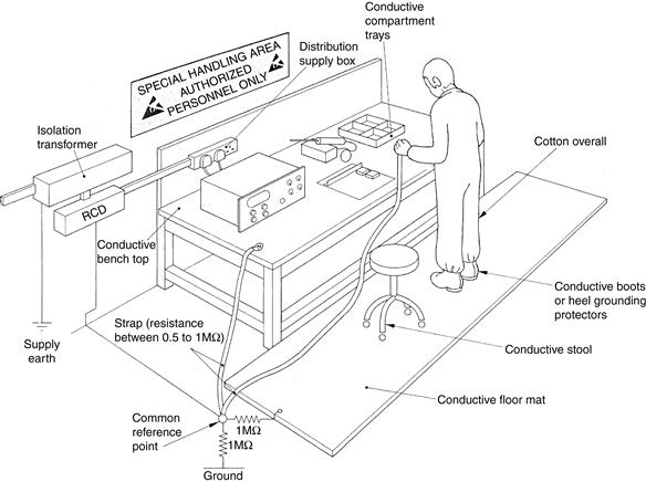
Figure 40.1 Static-safe workshop layout Extract from BS5783:1987 reproduced with the permission of BSI