
Chapter 36
Input and Output Parameters
36.1 Voltage
Typically you will be designing for 230V AC in the UK and continental Europe and 115V in the US. Other countries have frustratingly minor differences. The usual supply voltage variability is ±10%, or sometimes +10%/–15%. In the UK the supply authorities are obliged to maintain their voltage at the point of connection to the customer’s premises within ±6%, to which is added an allowance for local loading effects. If the voltage tolerance is applied to the UK/Europe nominal then the input voltage range becomes 207–253V or 195–253V. This range must be handled transparently by the power supply circuitry.
To cope simultaneously with both the American supply voltage, which may drop below 100V, and the European voltages is difficult for a linear supply although it is possible to design “universal” switch-mode circuits which can accept such a wide range (see the comment at the end of section 36.5). Historically, this problem was handled by using a mains transformer with a split primary (Figure 36.1) which can be connected in series or parallel by means of a discreetly mounted voltage selector switch. This has the disadvantage that the switch may be so discreet that the user doesn’t know about it, or else it may not be discreet enough and the user may be tempted to fiddle with it. This is not a real problem in the US, but applying 230V to a unit which is set for 115V will at least annoy the user by blowing a fuse, and at worst cause real damage. Universal switch-mode supplies are therefore popular.
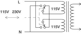
Figure 36.1 Split-primary transformer wiring
36.2 Current
The maximum continuous input current should be determined by the output load and the power conversion efficiency of the circuit. The main interest in this parameter is that it determines the rating of the input circuit components, especially the protective fuse. You have to decide whether an overload on the output will open the input circuit fuse or whether other protection measures, such as output current limiting, will operate. If the input fuse must blow, you need to characterize the input current very carefully over the entire range of input voltages. It is quite possible that the difference between maximum continuous current at full load, and minimum overload current at which the fuse should blow, is less than the fusing characteristics allow. Normally you need at least a 2:1 ratio between prospective fault current and maximum operating current. This may not be possible, in which case the input fuse protects the input circuit from faults only and some extra secondary circuit protection is necessary.
36.3 Fuses
A brief survey of fuse characteristics is useful here. The important characteristics that are specified by fuse manufacturers are the following:
• Rated current IN: that value by which the fuse is characterized for its application and which is marked on the fuse. For fuses to IEC 60127 this is the maximum value which the fuse can carry continuously without opening and without reaching too high a temperature, and is typically 60% of its minimum fusing current. For fuses to the American UL-198-G standard the rated current is 85–90% of its minimum fusing current, so that it runs hotter when carrying its rated current. The minimum fusing current is that at which the fusing element just reaches its melting temperature.
• Time-current characteristic: the pre-arcing time is the interval between the application of a current greater than the minimum fusing current and the instant at which an arc is initiated. This depends on the over-current to which the fuse is subjected and manufacturers will normally provide curves of the time-current characteristic, in which the fuse current is normalized to its rated current as shown in Figure 36.2. Several varieties of this characteristic are available:
T: time lag (or anti-surge, slow-blow)
Most applications can be satisfied with either type F or type T and it is best to specify these if at all possible, since replacements are easily obtainable. Type FF is mainly used for protecting semiconductor circuits.
The total operating time of the fuse is the sum of the pre-arcing time and the time for which the arc is maintained. Normally the latter must be taken into account only when interrupting high currents, typically more than ten times the rated current.
The energy in a short-duration surge required to open the fuse depends on I2t, and for pulse or surge applications you should consult the fuse’s published I2t rating. Current pulses that are not to open the fuse should have an I2t value less than 50–80% of the I2t value of the fuse.

Figure 36.2 Typical fuse time-current curves
• Breaking capacity: breaking capacity is the maximum current the fuse can interrupt at its rated voltage. The rated voltage of the fuse should exceed the maximum system voltage. To select the proper breaking capacity you need to know the maximum prospective fault current in the circuit to be protected – which is usually determined in mains-powered electronic products by the characteristics of the next fuse upstream in the supply. Cartridge fuses fall into one of two categories, high breaking capacity (HBC) which are sand-filled to quench the arc and have breaking capacities in the 1000s of amps, and low breaking capacity (LBC) which are unquenched and have breaking capacities of a few tens of amps or less.
36.4 Switch-on Surge, or Inrush Current
Continuous maximum input current is usually less than the input current experienced at switch-on. An unfortunate characteristic of mains power transformers is their low impedance when power is first applied. At the instant that voltage is applied to the primary, the current through it is limited only by the source resistance, primary winding resistance and the leakage inductance.
The effect is most noticeable on toroidal mains transformers when the mains voltage is applied at its peak halfway through the cycle, as in Figure 36.3. The typical mains supply has an extremely low source impedance, so that the only current limiting is provided by the transformer primary resistance and by the fuse. Toroidals are particularly efficient and can be wound with relatively few turns, so that their series resistance and leakage inductance is low; the surge current can be more than ten times the operating current of the transformer.† In these circumstances, the fuse usually loses out. The actual value of surge depends on where in the cycle the switch is closed, which is random; if it is near the zero crossing the surge is small or nonexistent, so it is possible for the problem to pass unnoticed if it is not thoroughly tested.

Figure 36.3 Switch-on surge
A separate component of this current is the abnormal secondary load due to the low impedance of the uncharged power supply reservoir capacitor. For the same reason, inrush current is also a problem in direct-off-line switch-mode supplies, where the reservoir capacitor is charged directly through the mains rectifier, and comparatively complex “soft-start” circuits may be needed in order to protect the input components.
Several simpler solutions are possible. One is to specify an anti-surge or time-lag (type T or TT) fuse. This will rupture at around twice its rated current if sustained for tens or hundreds of seconds, but will carry a short overload of ten or twenty times rated current for a few milliseconds. Even so, it is not always easy to size the fuse so that it provides adequate protection without eventually failing in normal use, particularly with the high ratios of surge to operating current that can occur. A resettable thermal circuit breaker is sometimes more attractive than a fuse, especially as it is inherently insensitive to switch-on surges.
36.4.1 Current Limiting
A more elegant solution is to use a negative-temperature-coefficient (NTC) thermistor in series with the transformer primary and fuse. The device has a high initial resistance which limits the inrush current but in so doing dissipates power, which heats it up. As it heats, its resistance drops to a point at which the power dissipated is just sufficient to maintain the low resistance and most of the applied voltage is developed across the transformer. The heating takes one or two seconds during which the primary current increases gradually rather than instantaneously.
NTC thermistors characterized especially for use as inrush current limiters are available, and can be used also for switch-mode power supply inputs, motor soft-start and filament lamp applications. Although the concept of an automatic current-limiter is attractive, there are three major disadvantages:
• because the devices operate on temperature rise they are difficult to apply over a wide ambient temperature range;
• they run at a high temperature during normal operation, so require ventilation and must be kept away from other heat-sensitive components; and
• they have a long cool-down period of several tens of seconds and so do not provide good protection against a short supply interruption.
36.4.2 PTC Thermistor Limiting
Another solution to the inrush current problem is to use instead a positive-temperature-coefficient thermistor in place of the fuse. These are characterized such that provided the current remains below a given value self-heating is negligible, and the resistance of the device is low. When the current exceeds this value under fault conditions the thermistor starts to self-heat significantly and its resistance increases until the current drops to a low value. Such a device does not protect against electric shock and so cannot replace a fuse in all applications, but because of its inherent insensitivity to surges it can be useful in local protection of a transformer winding.
A further more complex solution is to switch the AC input voltage only at the instant of zero crossing, using a triac. This results in a predictable switch-on characteristic, and may be attractive if electronic switching is required for other reasons such as standby control. Similarly, DC input supplies can use a power MOSFET to provide a controlled resistance at turn-on, as well as other circuitry such as reverse polarity protection and standby switching.
36.5 Waveform Distortion and Interference
36.5.1 Interference
Electrical interference generated within equipment and conducted out through the mains supply port was already subject to regulation for some product sectors in some countries, and with the adoption of the European EMC Directive it is mandatory for all electrical or electronic products to comply with interference limits. The usual method of reducing such interference is to use a radio frequency filter at the mains supply inlet, but good design practice also plays a substantial part. Switch-mode power supplies are normally the worst offenders, because they generate large interference currents at harmonics of the switching frequency well into the HF region. The size and weight advantages of switch-mode supplies are balanced by the need to fit larger filters to meet the interference limits.
36.5.2 Peak Current Summation
An increasing problem for electricity supply systems is the proportion of semiconductor-based equipment in the supply load. This is because the load current that such equipment takes is pulsed rather than sinusoidal. Current is only drawn at the peak of the input voltage, in order to charge the reservoir capacitors in the power supply. The normal RMS-to-average ratio of 1.11 for a sinusoidal current is considerably higher for this type of waveform (Figure 36.4).

Figure 36.4 Peak input current in a rectifier/reservoir power supply
The ratio of the peak load current Ipk to Irms is called the crest factor, and here it depends on the input impedance of the reservoir circuit. The lower the impedance, the faster the reservoir capacitor(s) will charge, which results in lower output voltage ripple but higher peak current.
The significance of crest factor is that it affects the power handling capability of the supply network. A network of a given sinusoidal RMS current rating will show considerable extra losses when faced with loads of a high crest factor. The supply mains does not have zero impedance, and the result of the extra network voltage drop at each crest is a waveform distortion in which the sinusoidal peak is flattened. This is a form of harmonic distortion and its seriousness depends on the susceptibility of other loads and components in the network.
Large systems installations, in which there are many electronic power supplies of fairly high rating fed from the same supply, are the main threat. In domestic premises, the switch-mode supplies of TV sets are the main offenders; in commercial buildings, the problem is worst with switch-mode supplies of PCs and their monitors, and fluorescent lamps with electronic ballasts. The current peaks always occur together and so reinforce each other. A network which is dominated by resistive loads such as heating and filament-lamp lighting can tolerate a proportion of high crest factor loads more easily.
36.5.3 Power Factor Correction
The “peakiness” of the input current waveform is best described in terms of its harmonic content and legislation now exists in Europe, under the EMC Directive, to control this. The European standard EN 61000-3-2:2000 places limits on the amplitude of each of the harmonic components of the mains input current up to the 40th (2 kHz at 50 Hz mains frequency), and it applies to virtually all electrical and electronic apparatus up to an input current of 16A, although products other than lighting equipment with a rated power of less than 75W are exempt. The limits, although not particularly stiff, are pretty much impossible for a switched-mode power supply to meet without some treatment of the input current. This treatment is generically known as power factor correction (PFC).
In this context, Power Factor (PF) is the ratio between the real power, as transferred through the power supply to its load with associated losses, and the apparent power drawn from the mains: RMS line voltage times RMS line current. A purely resistive load will have a PF of unity, but since peaks increase the RMS current, one drawing a peaky waveform will have a PF of 0.5–0.75. “Correcting” the PF toward unity requires that the input current waveform is made nearly sinusoidal, so that its harmonic content is much reduced. This is done by a second switching “pre-regulator” operating directly at the mains input. The usual topology is a boost regulator, as shown in Figure 36.5.

Figure 36.5 Power factor correction
The input rectifier supplies a full-wave-rectified half-sine voltage across CIN. This capacitor is too low a value to affect the 50 Hz input current significantly, but high enough to act as an effective reservoir at the switching frequency (typically 50–100 kHz). One sense input of the switching controller comes from this input voltage, and the controller is designed to maintain an average input current through the inductor in phase with this voltage. It does this by varying the switching pulse width or frequency as the input voltage changes. The rectified output is a DC voltage slightly higher than the highest peak supply voltage, which forms a reasonably well-regulated input to the main SMPS converter—which can of course be for any application, not just for an electronic power supply.
Naturally the addition of a second switching converter increases the cost of the total power supply, and contributes to more interference that must be filtered out at the mains input. Neither of these disadvantages are excessive, and commercial PFC power supply modules are now widely available. If you are designing your own, several IC manufacturers offer controllers specifically for the purpose, such as the L4981A/B, L6561, UC3853-5, and MC33626/33368. An extra advantage of the PFC pre-regulator is that almost by definition it will work over a wide input voltage range; so that a by-product of including it is that a single power supply will cover all worldwide markets, and will also have a uniform and predictable response to dips and interruptions.
36.6 Frequency
The UK and European mains frequency is held to 50 Hz ±1%. The American supply standard is 60 Hz. The difference in frequencies does not generally cause any problem for equipment that has to operate off either supply (provided that it’s designed in Europe!), since mains transformers and reservoir circuits that perform correctly at 50 Hz will have no difficulty at 60 Hz. The sensitivity of the power supply circuits to supply voltage droops at 60 Hz should be less than at 50Hz since the ripple amplitude is only 83% of the 50 Hz figure, and the minimum voltage will thus be higher (Figure 36.6).
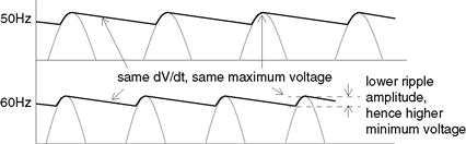
Figure 36.6 Ripple voltage vs. frequency
The ±1% tolerance on the mains frequency is slightly misleading because the supply authorities maintain a long-term tolerance very much better than this. Diurnal variations are arranged to cancel out, and this allows the mains to be used as a timing source for clocks and other purposes. If you are planning to use the mains frequency for internal timing then you will need to incorporate some kind of switching arrangement if the equipment will be used on both US and European systems.
36.7 Efficiency
The efficiency of a power supply module is its output power divided by its input power. The difference between the two quantities is accounted for by power losses in the various components in the power supply.
![]()
The efficiency normally worsens as the load is reduced, because the various losses and quiescent operating currents assume a greater proportion of the input power. Therefore, if you are concerned about efficiency, do not use a power supply that is heavily overrated for its purpose. Linear supply efficiency also varies considerably with its input voltage, being worst at high voltages, because the excess must be lost across the regulator. Switch-mode supplies do not have this problem.
Normally efficiency is not of prime concern for mains power supplies, since it is not essential to make optimum use of the available power, although at higher powers the heat generated by an inefficient unit can be troublesome. It is far more important that a power converter for a portable instrument should be efficient because this directly affects useable battery life.
Linear power supplies are rarely more than 50% efficient unless they can be matched to a narrow input voltage range, whereas switch-mode supplies can easily exceed 70% and with careful design can reach 90%. This makes switch-mode supplies more popular, despite their greater complexity, at the higher power levels and for battery-powered units.
36.7.1 Sources of Power Loss
The components in a power supply which make the major contribution to losses are:
| • the transformer: | core losses, determined by the operating level and core material, and copper losses, determined by I2R where R is the winding resistance |
| • the rectifiers: | diode forward voltage drop, VF, multiplied by operating current; more significant at low output voltages |
| • linear regulator: | the voltage dropped across the series pass element multiplied by the operating current; greatest at high input voltages |
| • switching regulator: | power dissipated in the switching element due to saturation voltage, plus switching losses in this and in snubber and suppressor components, proportional to switching frequency. |
If you sum the approximate contribution of each of these factors you can generally make a reasonable forecast of the efficiency of a given power supply design. The actual figure can be confirmed by measurement and if it is wildly astray then you should be looking for the cause.
36.8 Deriving the Input Voltage from the Output
In a linear supply with a series pass regulator element, the design must proceed from the minimum acceptable output voltage at maximum load current and minimum input voltage. These are the worst-case conditions and determine the input voltage step-down required. The minimum DC input voltage is given by the minimum output voltage plus all the tolerances and voltage drops in series:
![]()
where,
Vout(min) is the minimum acceptable output voltage
Vtol,reg is the regulator voltage tolerance, assuming it is not adjustable
Vseries,reg is the voltage drop across the regulator series pass element
Vseries, CS is the voltage drop across the current sense element if fitted
All the above parameters are specified at full load current. This value for Vin,dc is then the minimum input voltage allowed for a DC input supply, or it is the voltage at the minimum of the ripple trough for a rectified and smoothed AC input supply. This is related to the transformer secondary voltage as follows:
![]()
where,
Vripple is the peak ripple voltage across the reservoir capacitor
VD is the voltage drop across the rectifier diode(s)
Vtx is the RMS transformer secondary voltage
Vac(nom) is the specified transformer input voltage
The figure of 0.92 is an approximate allowance for full-wave rectifier efficiency with a single-capacitor reservoir. It can be more accurately derived using curves published by Schade†. Complications set in because the current drawn through the secondary is not sinusoidal, but occurs at the crest of the waveform (see section 36.5). The extra peak current reduces the peak secondary voltage from its quoted value, if this value is specified for a resistive load. You can get around this either by knowing the transformer’s losses in advance and allowing for the extra IR drop, or by specifying the transformer for a given circuit and letting the transformer supplier do the work for you, if you’re buying a custom component. The transformer secondary RMS current rating is determined by the rectifier configuration (Figure 36.7).
Take as an example a typical linear regulator circuit supplying 5V ±5% at 1A.
Here, Vout(min) is allowed to be 5V – 5% = 4.75V. The regulator we shall use is a standard 7805 type with ±4% tolerance and so Vtol,reg is 5V · 0.04 = 0.2V. Its specified minimum series voltage drop (or dropout voltage) at 1A and a junction temperature of 25°C (note the temperature restriction) is 2.5V maximum. The required minimum input voltage is:
![]()
If the peak ripple voltage is 2V and each diode forward drop in the bridge is 1V, then the transformer voltage with a 240V nominal spec but a minimum line voltage of 195V will need to be:
![]()

Figure 36.7 Rectifier configuration
From this example you can see that the secondary-side input voltage needed to assure a given output voltage is very much higher than the actual output voltage. One of the major culprits is the dropout voltage of the regulator which in this example accounts for at least 50% of the output power, although it becomes proportionally less at higher output voltages. Low-dropout voltage regulators which use a PNP transistor as the series pass element, such as National Semiconductor’s LM2930 range, are popular for this reason and also where the minimum input voltage can be close to the output level, as in automotive applications.
36.8.1 Power Losses at High Input Voltage
You can also see more clearly in the above example where the power losses are which contribute to reduced efficiency. When the input voltage is increased to its maximum value the dissipation in the series-pass element is worst. In the above example with the mains input at 264V, the average value of Vin,dc rises to 12.5V, and 7.45V of this must be lost across the regulator, which because it is passing the full load current amounts to one-and-a-half times the load power! The advantage of the switch-mode supply is that it adjusts to varying input voltages by modifying its switching duty cycle, so that an increased input voltage automatically reduces the input current and the overall power taken by the unit remains roughly constant.
36.9 Low-Load Condition
When the output load is removed or substantially reduced then the dissipation in the power supply will drop. This is good news for almost all parts of the circuit, except for the voltage rating of the components around Vin,dc. When there is a combination of low load and maximum supply input voltage, the peak value of Vin,dc is highest. A crucial factor here is the transformer regulation. This is the ratio:
![]()
and a small or poorly-designed transformer can have a regulation exceeding 20%. If this figure is used for the transformer in the above example then the peak Vtx off-load at maximum input voltage will rise to 20.2V. At the same time the diode forward voltage drops at low current will be much less, say 0.6V each, so the possible maximum voltage at the reservoir capacitor could be around 19V. Thus even the common 16V rated electrolytic will not be adequate for this circuit. For higher voltage outputs, the maximum input voltage can even exceed the voltage rating of the regulator itself, and you have to invest in a pre-regulator to hold the maximum to a manageable level. Note that this condition is not the worst-case for regulator power dissipation, because the regulator is not passing significant load current.
36.9.1 Maximum Regulator Dissipation
In fact maximum series-pass dissipation does not necessarily occur at full load current, because as the current rises the voltage across the series-pass element falls. The maximum dissipation will occur at less than full output if the voltage dropped across the DC supply’s equivalent series resistance is greater than half the difference between the no-load input voltage and the output voltage. Figure 36.8 shows this graphically.

Figure 36.8 Peak power dissipation
36.9.2 Minimum Load Requirement
A further problem, particularly with switch-mode supplies, is that the stability of the regulator cannot always be assured down to zero load. For this reason some rails have to be run with a minimum load, such as a bleed resistor, to remain within specification, and this represents an unnecessary additional power drain. Many circuits, of course, always take a minimum current and so the minimum load is not then a problem.
36.10 Rectifier and Capacitor Selection
The specification of the rectifiers and capacitors is dominated by surge and ripple current concerns.
36.10.1 Reservoir capacitor
The minimum capacitor value is easily decided from the required ripple voltage:
![]()
where,
Vripple is the acceptable ripple voltage
For mains inputs, t is about 2 ms less than the AC input period, 8 ms for 50 Hz or
A more accurate value can be derived from Schade’s curves (see previous footnote) which have been reprinted in numerous textbooks, but remember that the tolerance on reservoir capacitors is wide (typically ±20%) and accuracy is rarely needed.
For load currents exceeding 1A, ripple current rating tends to determine capacitor selection rather than ripple voltage. As is made clear throughout this chapter, the peak current flow through the rectifier/capacitor circuit is many times higher than the DC current, due to the short time in each cycle for which the capacitor is charging. The RMS ripple current is 2–3 times higher than the DC load. Ripple current rating is directly related to temperature and you may need to derate the component further if you need high ambient temperature and/or high reliability operation.
As an example, a load current of 2A and a permissible ripple voltage of 3V at 100 Hz suggests a 5300 μF capacitor. Typical capacitors of the next value up from this, 6800 μF, have 85°C ripple current ratings from 2 to 4A. The higher ratings are larger and more expensive. But actual ripple current requirements will be 4–6A. To meet this you will need to use either a much larger capacitor (typically 22,000 μF), or two smaller capacitors in parallel, or derate the operating temperature and use a slightly larger capacitor. If you don’t do this, your design will become yet another statistic to prove that electrolytic capacitors are the prime cause of power supply failure.
36.10.2 Rectifiers
Although in the full-wave arrangements (Figure 36.7) the diodes only conduct on alternate half cycles, because the RMS current is 2–3 times higher than the DC load current a rating of at least the full load current, and preferably twice it, is necessary. Surge current on turn-on may be much higher, especially in the higher power supplies where the ratio of reservoir capacitance to operating current is increased. This is of even greater concern in direct-off-line switch-mode supplies where there is no transformer series resistance to limit the surge, and a diode rating of up to 5 times the average DC current is needed.
The maximum instantaneous surge current is Vmax/Rs and the capacitor charges with a time constant of τ = C·Rs, where Rs is the circuit series resistance. As a conservative guide, the surge won’t damage the diode if τ is less than a half-cycle at mains frequency and Vmax/Rs is less than the diode’s rated IFSM. All diode manufacturers publish IFSM ratings for a given time constant; for example, the typical 1N5400 series with 3A average rating have an IFSM of 200A. You may discover that you have to incorporate a small extra series resistance to limit the surge current, or use a larger diode, or apply the techniques discussed in section 36.4.
The rectifier’s peak-inverse-voltage (PIV) rating needs to be at least equivalent to the peak AC voltage for the full-wave bridge circuit, or twice this for the full-wave centre tap. But you should increase this considerably (by 50 to 100%) to allow for line transients. This is easy for low-voltage circuits, since 200V diodes cost hardly any more than 50V ones, and does not normally make much cost difference in mains circuits. For 240V, a minimum of 600V PIV and preferably 800V PIV should be specified, even if you are using a transient suppressor at the input.
36.11 Load and Line Regulation
Load regulation refers to the permissible shift in output voltage when the load is varied, usually from none to full. Line (or input) regulation similarly refers to the permissible shift in output voltage when the input is varied, usually from maximum to minimum. Provided that the design of the input circuit has been properly considered as described above, so that the input voltage never goes outside the regulator’s operational range, these parameters should be wholly a function of the regulator circuit itself. The regulator is essentially a feedback circuit which compares its output voltage against a reference voltage, so the regulation depends on two parameters: the stability of the reference, and the gain of the feedback error amplifier. If you use a monolithic regulator IC, then these factors are taken into account by the manufacturer who will specify regulation as a data sheet parameter.
36.11.1 Thermal Regulation
A monolithic regulator IC includes the voltage reference on-chip, along with other circuitry and the series pass element. This means that the reference is subject to a thermal shift when the power dissipation of the series pass element changes. This gives rise to a separate longer term component of regulation, called thermal regulation, defined as the change in output voltage caused by a change in dissipated power for a specified time. Provided the chip has been well-designed, thermal regulation is not a significant factor for most purposes, but it is rarely specified in data sheets and for some precision applications may render monolithic regulators unsuitable.
36.11.2 Load Sensing
No three-terminal regulator can maintain a constant voltage at anywhere other than its output terminals. It is common in larger systems for the load to be located at some distance from the power supply module, so that load-dependent voltage drops occur in the wiring connecting the load to the power supply output. This directly impacts the achievable load regulation.
The accepted way to overcome this problem is to split the regulator feedback path, and incorporate two extra “sensing” terminals which are connected so as to sense the output voltage at the load itself (Figure 36.9). The voltage drop across this extra pair of wires is negligible because they only carry the signal current. The voltage at the regulator output is adjusted so as to regulate the voltage at the sensing terminals.

Figure 36.9 Load sensing
The minimum voltage at the regulator input must be increased to allow for the extra output voltage drop. It is wise to connect coupling resistors (shown shaded in Figure 36.9) from the output to sense terminals, so as to ensure correct operation when the sense terminals are accidentally or deliberately disconnected. Sensing can only offer remote load regulation at one point and so is not really suited when one power supply module feeds several loads at different points.
36.12 Ripple and Noise
Ripple is the component of the AC supply frequency (or more often its second harmonic) which is present on the output voltage; noise is all other AC contamination on the output. In a linear power supply, ripple is the predominant factor and is given by the AC across the reservoir capacitor reduced by the ripple rejection (typically 70–80 dB) of the regulator circuit. A figure of less than 1 mV RMS should be easy to obtain. HF noise is filtered by the reservoir and output capacitors and there are no significant internal noise sources, provided that the regulator isn’t allowed to oscillate, so that apart from supply-frequency ripple linear power supplies are very “quiet” units.
36.12.1 Switching Noise
The same cannot be said for switch-mode power supplies. Here the noise is mainly due to output voltage spikes at the switching frequency, caused by fast-rise-time edges and HF ringing at these edges feeding through, or past, filtering components to the output. The ESR and ESL of typical output filter capacitors limits their ability to attenuate these spikes, while the self-inductance of ground wiring limits the high frequency effectiveness of ground decoupling anyway. Switch-mode output ripple and noise is typically 1% of the rail voltage, or 100–200 mV. In fact comparing ripple and noise specifications is the easiest way to distinguish a linear from a switch-mode unit, if there is no other obvious indication. The bandwidth over which the specification applies is important, since there is significant energy in the high-order harmonics of the switching noise, and at least 10 MHz is needed to get a true picture. Because of stray coupling over this extended bandwidth the noise frequently appears in common mode, on both supply and 0V simultaneously, and is then very difficult to control. Differential mode noise spikes can be reduced dramatically by including a ferrite bead in series, and a small ceramic capacitor in parallel with the output capacitor.
The presence of switching noise is not a problem for digital circuits, but it creates difficulties for sensitive analog circuits if their bandwidth exceeds the switching frequency. It can cause interference on video signals, mis-clocking in pulse circuits and voltage shifts in DC amplifiers. These effects have to be treated as EMC phenomena and can be cured by suitable layout, filtering and shielding, but if you have the option in the early stages to choose a linear supply instead, take it—you will save yourself a lot of trouble.
36.12.2 Layout to Avoid Ripple
Power supply output ripple is aggravated by incorrect layout of the wiring around the reservoir capacitor.
At first sight, grounds A and B in Figure 36.10 look equivalent. But there will be a potential between them of IR · Rg, where IR is the capacitor ripple current and Rg is the track or wiring resistance common to the two grounds through which the ripple current flows. (The ripple current path is through the transformer, the two diodes and the capacitor.) This current is only drawn on peaks of the AC input waveform to charge the reservoir capacitor, and its magnitude is only limited by the combined series resistance of the transformer winding, the diodes, capacitor and track or wiring. If the steady-state DC current supplied is 1A then the peak ripple current may be of the order of 5A; thus, 10 mΩ of Rg will give a peak difference of 50 mV between grounds A and B. If some parts of the circuit are grounded to A and some to B, then tens of millivolts of hum injection are included in the design at no additional cost, and increasing the reservoir value to try and reduce it will actually make matters worse as the peak ripple current is increased. You can check the problem easily, by observing the output ripple on a ’scope; if it has a pulse shape then wiring is the problem, if it looks more like a sawtooth then you need more smoothing.
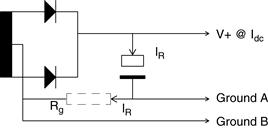
Figure 36.10 Incorrect reservoir connection
36.12.3 Correct Reservoir Connection
The solution to this problem, and the correct design approach, is to ground all parts of the supplied circuit on the supply side of the reservoir capacitor, so that the ripple current ground path is not common to any other part of the circuit (Figure 36.11). The same applies to the V+ supply itself. The common impedance path is now reduced to the capacitor’s own ESR, which is the best you can do.

Figure 36.11 Correct reservoir connection
36.13 Transient Response
The transient response of a power supply is a measure of how fast it reacts to a sudden change in load current. This is primarily a function of the bandwidth of the regulator’s feedback loop. The regulator has to maintain a constant output in the face of load changes, and the speed at which it can do this is set by its frequency response as with any conventional operational amplifier. The trade-off that the power supply designer has to worry about is against the stability of the regulator under all load conditions; a regulator with a very fast response is likely to be unstable under some conditions of load, and so its bandwidth is “slugged” by a compensation capacitor within the regulator circuit. Too much of this and the transient response suffers. The same effect can be had by siting a large capacitor at the regulator output, but this is a brute-force and inefficient approach because its effect is heavily load-dependent. Note that the 78XX series of three-terminal regulators should have a small, typically 0.1 μF capacitor at the output for good transient response and HF noise decoupling. This is separate from the required 0.33–1 μF capacitor at the input to ensure stability.

Figure 36.12 Load transient response
36.13.1 Switch-Mode vs. Linear
The transient response of a switch-mode power supply is noticeably worse than that of a linear because the bandwidth of the feedback loop has to be considerably less than the switching frequency. Typically, switch-mode transient recovery time is measured in milliseconds while linear is in the tens of microseconds.
If your circuit only presents slowly-varying loads then the power supply’s transient response will not interest you. It becomes important when a large proportion of the load can be instantaneously switched—a relay coil or bank of LEDs for example—and the rest of the load is susceptible to short-duration over- or undervoltages.
Although load transient response is usually the most significant, a regulator also exhibits a delayed response to line transients, and this may become important when you are feeding it from a DC input which can change quickly. The line transient response is normally of the same order as the load response.