
Chapter 7
Digital Circuit Fundamentals
Early electronic circuits were analog, and before the advent of digital logic, signal processing was undertaken using analog electronic circuits. The invention of the semiconductor transistor in 1947 at Bell Laboratories [Ref. 7.1] and the improvements in transistor characteristics and fabrication during the 1950s led to the introduction of linear (analog) ICs and the first transistor-transistor logic (TTL) digital logic IC in the early 1960s, closely followed by complementary metal-oxide semiconductor (CMOS) ICs. The early devices incorporated a small number of logic gates. However, rapid growth in the ability to fabricate an increasing number of logic gates in a single IC led to the microprocessor in the early 1970s. This, with the ability to create memory ICs with ever increasing capacities, laid the foundation for the rapid expansion in the computer industry and the types of complex digital systems based on the computer architecture that we have available today. The last fifty years have seen a revolution in the electronics industry.
Fundamentally, a digital circuit will be categorized into one of three general types, each of which is created and fabricated within an integrated circuit:
• Combinational logic, in which the response of the circuit is based on a Boolean logic expression of the input only and the circuit responds immediately to a change in the input.
• Sequential logic, in which the response of the circuit is based on the current state of the circuit and the sometimes the current input. This may be asynchronous or synchronous. In synchronous sequential logic, the logic changes state whenever an external clock control signal is applied. In asynchronous sequential logic, the logic changes state on changes of the input data (the circuit does not utilize a clock control signal).
• Memory, in which digital values can be stored and retrieved some time later. For a user, memory can be either read-only (ROM) or random-access (RAM). In ROM, the data stored in the memory are initially placed in the memory and can only be read by the user. Data cannot normally be altered in the circuit application. In RAM (also referred to as read-write memory, RWM), the user can write data to the memory and read the data back from the memory.
The digital IC consists of a number of logic gates, which are combinational or sequential circuit elements. The logic gates may be implemented using different fabrication processes and different circuit architectures:
• TTL, transistor-transistor logic (bipolar)
• ECL, emitter-coupled logic (bipolar)
The material predominantly used to fabricate the digital logic circuits is silicon. However, silicon-based circuits are complemented with the digital logic capabilities of circuits fabricated using gallium arsenide (GaAs) and silicon germanium (SiGe) technologies. Today, silicon-based CMOS is by far the dominant process used for digital logic.
The digital logic gate is actually an abstraction of what is happening within the underlying circuit. All digital logic gates are made up of transistors. The logic gates may take one of a number of different circuit architectures (the way in which the transistors are interconnected) at the transistor level:
Today, static CMOS logic is by far the dominant logic cell design structure used. The number of logic gates within a digital logic IC will range from a few to hundreds of thousands and ultimately millions for the more complex processors and PLDs. In previous times, when the potential for higher levels of integration was far less than is now possible, the digital IC was classified by the level of integration—that is, the number of logic gate equivalents per IC (see Table 7.1). With increasing levels of integration, the following levels were identified as follow-on descriptions from VLSI, but these are not in common usage:
Table 7.1 Levels of integration
| Level of integration | Acronym | Number of gate equivalents per IC |
| Small-scale integration | SSI | <10 |
| Medium-scale integration | MSI | 10–100 |
| Large-scale integration | LSI | 100–10,000 |
| Very large-scale integration | VLSI | >10,000 |
The equivalent logic gate consists of four transistors. In static CMOS logic, the 2-input NAND and 2-input NOR are four transistor logic gate structures (2 nMOS +2 pMOS transistors). Figure 7.1 shows the 2-input NAND and NOR gate in static CMOS with both the digital logic gate symbol and the underlying transistor level circuit. At the transistor level, the circuit is connected to a power supply (VDD = positive power supply voltage and VSS = negative power supply voltage). The nMOS transistors are connected toward VSS and the pMOS transistors toward VDD.

Figure 7.1 Two-input NAND and NOR gates
7.1 Digital Technology
In the digital domain, the choice of implementation technology is essentially whether to use dedicated- (and fixed-) functionality digital logic, to use a software-programmed processor based system (microprocessor, μP; microcontroller, μC; or digital signal processor, DSP), or to use a hardware-configured programmable logic device (PLD) such as the simple programmable logic device (SPLD), complex programmable logic device (CPLD), or the field-programmable gate array (FPGA). Memory—random access memory (RAM) or read-only memory (ROM)—is also widely used in many digital electronic circuits and systems. The choices are shown in Figure 7.2.
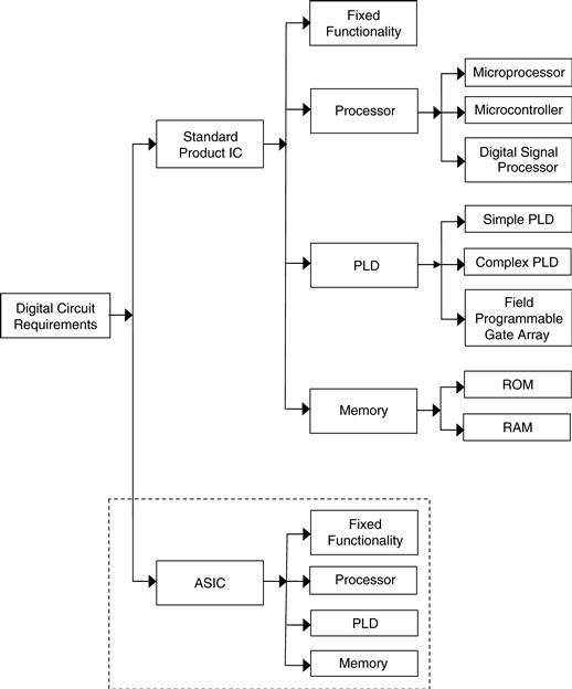
Figure 7.2 Technology choices for digital circuit design
The initial choice for implementing the digital circuit is between a standard product IC (integrated circuit) and an ASIC (application-specific integrated circuit) [Ref. 7.2]:
• Standard product IC, an off-the-shelf electronic component that has been designed and manufactured for a given purpose, or range of use, and that is commercially available. It is purchased either from a component supplier or directly from the designer or manufacturer.
• ASIC, an integrated circuit that has been specifically designed and manufactured for a particular application.
For many applications, developing an electronic system based on standard product ICs is more cost effective than ASIC design. Undertaking an ASIC design project also requires access to IC design experience, IC computer-aided design (CAD) tools, and a suitable manufacturing and test capability. Whether a standard product IC or ASIC design approach is taken, the type of IC used or developed will be one of four types:
1. Fixed-functionality: These ICs have been designed to implement a specific functionality and cannot be changed. The designer uses a set of these ICs to implement a given overall circuit functionality. Changes to the circuit require a complete redesign of the circuit and the use of different fixed functionality ICs.
2. Processor: Most people are familiar with processors in everyday use; the heart of the PC is a microprocessor. This component runs a software program to implement a required functionality. By changing the software program, the processor will operate a different function. The three types of processor are microprocessor (μP), microcontroller (μC), and digital signal processor (DSP).
3. Memory: Memory is used to store, provide access to, and allow modification of data and program code for use within a processor-based electronic circuit/system. The two types of memory are ROM (read-only memory) and RAM (random access memory). ROM is used for holding program code that must be retained when the memory power is removed; this is nonvolatile storage. The code can either be fixed when the memory is fabricated (mask programmable ROM), electrically programmed once (PROM, programmable ROM) or electronically programmed multiple times. Multiple programming capacity requires the ability to erase prior programming, which is available with EPROM (electrically programmable ROM, erased using ultraviolet [UV] light), EEPROM or E2PROM (electrically erasable PROM), or Flash (also electrically erased). PROM is sometimes considered to be in the same category of circuit as simple programmable logic device (SPLD), although in this text, PROM is considered in the memory category only. RAM is used for holding data and program code that require fast access and the ability to modify the contents during normal operation. RAM differs from read-only memory (ROM) in that it can be both read from and written to in the normal circuit application. However, Flash memory can also be referred to as nonvolatile RAM (NVRAM). RAM is considered to provide a volatile storage since, unlike ROM, the contents of RAM are lost when the power is removed. There are two main types of RAM: static RAM (SRAM) and dynamic RAM (DRAM).
4. PLD: The programmable logic device is an IC that contains digital logic cells and programmable interconnect [Refs. 7.3, 7.4] to enable the designer to configure the logic cells and interconnect within the IC itself to form a digital electronic circuit within a single packaged IC. In this, the hardware resources (the available hardware for use) are configured to implement the required functionality. By changing the hardware configuration, the PLD performs a different function. Three types of PLD are available: the simple programmable logic device (SPLD), the complex programmable logic device (CPLD), and the field-programmable gate array (FPGA).
Both the processor and PLD enable the designer to implement and change the functionality of the IC by either changing the software program or the hardware configuration. To avoid potential confusion, the following terms are used to differentiate the PLD from the processor:
• The PLD will be configured using a hardware configuration.
• The processor will be programmed using a software program.
An ASIC can be designed to create any one of the four standard product IC forms (fixed-functionality, processor, memory, or PLD). A standard product IC is designed in the same manner as an ASIC, so anyone who has access to an ASIC design, fabrication, and test facility can create an equivalent to a standard product IC (given that patents and legal issues of IP [intellectual property] for existing designs and devices are taken into account).
No matter how complex the digital circuit design, and the types of operations it is required to undertake, the operation is based on a small number of basic combinational and sequential logic circuit elements that are connected to form the required circuit operation:
• Combinational logic: A combinational logic circuit is defined by a Boolean expression, and the output from the circuit (in logic terms) is a function of the logic input values, the logic gates used (AND, OR, etc.), and the way in which the logic gates are connected [Refs. 7.5, 7.6]. The output becomes a final value when the inputs change after a finite time, which is the time required for the logic values to propagate through the circuit given signal propagation delays in each of the logic gates and any delays in the interconnections between the logic gates. The basic combinational logic circuit elements (gates) are:
• Sequential logic: In a sequential logic circuit, the output from the circuit becomes a value based on the logic input values, the logic gates used, the way in which the logic gates are connected, and on the current state of the circuit [Refs. 7.5, 7.6]. In a synchronous sequential logic circuit, the output change occurs either on the edge of a clock signal change (from 0 to 1 or from 1 to 0) or on a clock signal level (logic 0 or 1). However, an asynchronous sequential logic circuit does not use a clock input. In the sequential logic circuit, the circuit will hold or remember its current value (state) and will change state only on clock or data changes. A sequential logic circuit might also contain additional control signals to reset or set the circuit into a known state either when the circuit is initially turned on or during normal circuit operation. The basic sequential logic circuit elements (gates) are:
REFERENCES
[7.1] Bell Laboratories (Bell Labs), http:www.bell-labs.com/.
[7.2] Smith M. Application Specific Integrated Circuits Addison-Wesley 1999; ISBN 0-201-50022-1.
[7.3] Skahill K. VHDL for Programmable Logic. Addison-Wesley 1996; ISBN 0-201-89573-0.
[7.4] Maxfield C. The Design Warrior’s Guide to FPGAs Newnes 2004; ISBN 0-7506-7604-3.
[7.5] Stonham TJ. Digital Logic Techniques: Principles and practice Second Edition UK: Van Nostrand Reinhold; 1988; ISBN 0-278-00011-8.
[7.6] Tocci RJ, Widmer NS, Moss GLK. Digital Systems Ninth Edition USA: Pearson Education International; 2004; ISBN 0-13-121931-6.