
DRAM Memory Controller
In modern computer systems, processors and I/O devices access data in the memory system through the use of one or more memory controllers. Memory controllers manage the movement of data into and out of DRAM devices while ensuring protocol compliance, accounting for DRAM-device-specific electrical characteristics, timing characteristics, and, depending on the specific system, even error detection and correction. DRAM memory controllers are often contained as part of the system controller, and the design of an optimal memory controller must consist of system-level considerations that ensure fairness in arbitration for access between different agents that read and store data in the same memory system.
The design and implementation of the DRAM memory controllers determine the access latency and bandwidth efficiency characteristics of the DRAM memory system. The previous chapters provide a bottom-up approach to the design and implementation of a DRAM memory system. With the understanding of DRAM device operations and system level provided by the previous chapters, this chapter proceeds to examine DRAM controller design and implementation considerations.
13.1 DRAM Controller Architecture
The function of a DRAM memory controller is to manage the flow of data into and out of DRAM devices connected to that DRAM controller in the memory system. However, due to the complexity of DRAM memory-access protocols, the large numbers of timing parameters, the innumerable combinations of memory system organizations, different workload characteristics, and different design goals, the design space of a DRAM memory controller for a given DRAM device has nearly as much freedom in the design space as the design space of a processor that implements a specific instruction-set architecture. In that sense, just as an instruction-set architecture defines the programming model of a processor, a DRAM-access protocol defines the interface protocol between a DRAM memory controller and the system of DRAM devices. In both cases, actual performance characteristics depend on the specific microarchitectural implementations rather than the superficial description of a programming model or interface protocol. That is, just as two processors that support the same instruction-set architecture can have dramatically different performance characteristics depending on the respective microarchitectural implementations, two DRAM memory controllers that support the same DRAM-access protocol can have dramatically different latency and sustainable bandwidth characteristics depending on the respective microarchitectural implementations. DRAM memory controllers can be designed to minimize die size, minimize power consumption, maximize system performance, or simply reach a reasonably optimal compromise of the conflicting design goals. Specifically, the Row-Buffer-Management Policy, the Address Mapping Scheme, and the Memory Transaction and DRAM Command Ordering Scheme are particularly important to the design and implementation of DRAM memory controllers.
Due to the increasing disparity in the operating frequency of modern processors and the access latency to main memory, there is a large body of active and ongoing research in the architectural community devoted to the performance optimization of the DRAM memory controller. Specifically, the Address Mapping Scheme, designed to minimize bank address conflicts, has been studied by Lin et al. [2001] and Zhang et al. [2002a]. DRAM Command and Memory Transaction Ordering Schemes have been studied by Briggs et al. [2002], Cuppu et al. [1999], Hur and Lin [2004], McKee et al. [1996a], and Rixner et al. [2000]. Due to the sheer volume of research into optimal DRAM controller designs for different types of DRAM memory systems and workload characteristics, this chapter is not intended as a comprehensive summary of all prior work. Rather, the text in this chapter describes the basic concepts of DRAM memory controller design in abstraction, and relevant research on specific topics is referenced as needed.
Figure 13.1 illustrates some basic components of an abstract DRAM memory controller. The memory controller accepts requests from one or more microprocessors and one or more I/O devices and provides the arbitration interface to determine which request agent will be able to place its request into the memory controller. From a certain perspective, the request arbitration logic may be considered as part of the system controller rather than the memory controller. However, as the cost of memory access continues to increase relative to the cost of data computation in modern processors, efforts in performance optimizations are combining transaction scheduling and command scheduling policies and examining them in a collective context rather than separate optimizations. For example, a low-priority request from an I/O device to an already open bank may be scheduled ahead of a high-priority request from a microprocessor to a different row of the same open bank, depending on the access history, respective priority, and state of the memory system. Consequently, a discussion on transaction arbitration is included in this chapter.
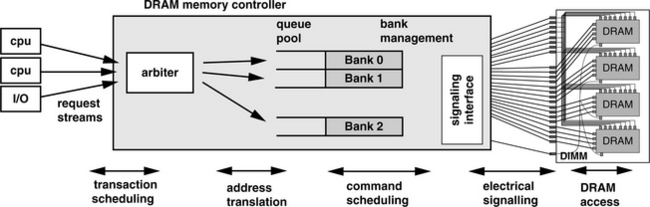
Figure 13.1 also illustrates that once a transaction wins arbitration and enters into the memory controller, it is mapped to a memory address location and converted to a sequence of DRAM commands. The sequence of commands is placed in queues that exist in the memory controller. The queues may be arranged as a generic queue pool, where the controller will select from pending commands to execute, or the queues may be arranged so that there is one queue per bank or per rank of memory. Then, depending on the DRAM command scheduling policy, commands are scheduled to the DRAM devices through the electrical signaling interface.
In the following sections, the various components of the memory controller illustrated in Figure 13.1 are separately examined, with the exception of the electrical signaling interface. Although the electrical signaling interface may be one of the most critical components in modern, high data rate memory systems, the challenges of signaling are examined separately in Chapter 9. Consequently, the focus in this chapter is limited to the digital logic components of the DRAM memory controller.
13.2 Row-Buffer-Management Policy
In modern DRAM devices, the arrays of sense amplifiers can also act as buffers that provide temporary data storage. In this chapter, policies that manage the operation of sense amplifiers are referred to as row-buffer-management policies. The two primary row-buffer-management policies are the open-page policy and the close-page policy, and depending on the system, different row-buffer-management policies can be used to optimize performance or minimize power consumption of the DRAM memory system.
13.2.1 Open-Page Row-Buffer-Management Policy
In commodity DRAM devices, data access to and from the DRAM storage cells is a two-step process that requires separate row activation commands and column access commands.1 In cases where the memory-access sequence possesses a high degree of temporal and spatial locality, memory system architects and design engineers can take advantage of the locality by directing temporally and spatially adjacent memory accesses to the same row of memory. The open-page row-buffer-management policy is designed to favor memory accesses to the same row of memory by keeping sense amplifiers open and holding a row of data for ready access. In a DRAM controller that implements the open-page policy, once a row of data is brought to the array of sense amplifiers in a bank of DRAM cells, different columns of the same row can be accessed again with the minimal latency of tCAS. In the case where another memory read access is made to the same row, that memory access can occur with minimal latency since the row is already active in the sense amplifier and only a column access command is needed to move the data from the sense amplifiers to the memory controller. However, in the case where the access is to a different row of the same bank, the memory controller must first precharge the DRAM array, engage another row activation, and then perform the column access.
13.2.2 Close-Page Row-Buffer-Management Policy
In contrast to the open-page row-buffer-management policy, the close-page row-buffer-management policy is designed to favor accesses to random locations in memory and optimally supports memory request patterns with low degrees of access locality. The open-page policy and closely related variant policies are typically deployed in memory systems designed for low processor count, general-purpose computers. In contrast, the close-page policy is typically deployed in memory systems designed for large processor count, multiprocessor systems or specialty embedded systems. The reason that an open-page policy is typically deployed in memory systems of low processor count platforms while a close-page policy is typically deployed in memory systems of larger processor count platforms is that in large systems, the intermixing of memory request sequences from multiple, concurrent, threaded contexts reduces the locality of the resulting memory-access sequence. Consequently, the probability of row hit decreases and the probability of bank conflict increases in these systems, reaching a tipping point of sorts where a close-page policy provides better performance for the computer system. However, not all large processor count systems use close-page memory systems. For example, Alpha EV7’s Direct RDRAM memory system uses open-page policy to manage the sense amplifiers in the DRAM devices. The reason for this choice is that a fully loaded Direct RDRAM memory system has 32 ranks of DRAM devices per channel and 32 split banks per rank. The large number of banks in the Direct RDRAM memory system means that even in the case where a large number of concurrent processes are accessing memory from the same memory system, the probability of bank conflicts remains low. Consequently, Alpha EV7’s memory system demonstrates that the optimality in the choice of row-buffer-management policies depends on both the type and the number of the processor, as well as the parallelism available in the memory system.
13.2.3 Hybrid (Dynamic) Row-Buffer-Management Policies
In modern DRAM memory controllers, the row-buffer-management policy is often neither a strictly open-page policy nor a strictly close-page policy, but a dynamic combination of the two policies. That is, the respective analyses of the performance and power consumption impact of row-buffer-management policies illustrate that the optimality of the row-buffer-management policy depends on the request rate and access locality of the memory request sequences. To support memory request sequences whose request rate and access locality can change dramatically depending on the dynamic, run-time behavior of the workload, DRAM memory controllers designed for general-purpose computing can utilize a combination of access history and timers to dynamically control the row-buffer-management policy for performance optimization or power consumption minimization.
Previously, the minimum ratio of memory read requests that must be row buffer hits for an open-page memory system to have lower read latency than a comparable close-page memory system was computed as tRP / (tRCD + tRP). The minimum ratio of row buffer hits means that if a sequence of bank conflicts occurs in rapid succession and the ratio of memory read requests that are row buffer hits falls below a precomputed threshold, the DRAM controller can switch to a close-page policy for better performance. Similarly, if a rapid succession of memory requests to a given bank is made to the same row, the DRAM controller can switch to an open-page policy to improve performance. One simple mechanism used in modern DRAM controllers to improve performance and reduce power consumption is the use of a timer to control the sense amplifiers. That is, a timer is set to a predetermined value when a row is activated. The timer counts down with every clock tick, and when it reaches zero, a precharge command is issued to precharge the bank. In case of a row buffer hit to an open bank, the counter is reset to a higher value and the countdown repeats. In this manner, temporal and spatial locality present in a given memory-access sequence can be utilized without keeping rows open indefinitely.
Finally, row-buffer-management policies can be controlled on a channel-by-channel basis or on a bank-by-bank basis. However, the potential gains in performance and power savings must be traded off against the increase in hardware sophistication and design complexity of the memory controller. In cases where high performance or minimum power consumption is not required, a basic controller can be implemented to minimize die size impact of the DRAM memory controller.
The definition of the row-buffer-management policy forms the foundation in the design of a DRAM memory controller. The choice of the row-buffer-management policy directly impacts the design of the address mapping scheme, the memory command reordering mechanism, and the transaction reordering mechanism in DRAM memory controllers. In the following sections, the address mapping scheme, the memory command reordering mechanism, and the transaction reordering mechanism are explored in the context of the row-buffer-management policy used.
13.2.4 Performance Impact of Row-Buffer-Management Policies
A formal analysis that compares the performance of row-buffer-management policies requires an in-depth analysis of system-level queuing delays, the locality and rate of request arrival in the memory-access sequences. However, a first-order approximation of the performance benefits and trade-offs of different policies can be made through the analysis of memory read access latencies. Assuming nominally idle systems, the read latency in a close-page memory system is simply tRCD + tCAS. Comparably, the read latency in an open-page memory system is as little as tCAS or as much as tRP + tRCD + tCAS.2 In this context, tCAS is the row buffer hit latency, and tRP + tRCD + tCAS is the row buffer miss (bank conflict) latency. If x represents the percentage of memory accesses that hit in an open row buffer, and 1 – x represents the percentage of memory accesses that miss the row buffer, the average DRAM-access latency in an open-page memory system is x * (tCAS) + (1 – x) * (tRP + tRCD + tCAS). Taking the formula and equating to the memory read latency of tRCD + tCAS in a close-page memory system, the minimum percentage of memory accesses that must be row buffer hits for an open-page memory system to have lower average memory-access latency than a close-page memory system can be solved for.
Solving for x, the minimum ratio of memory read requests that must be row buffer hits for an open-page memory system to have lower read latency is simply tRP/(tRCD + tRP). That is, as tRP approaches infinity,3 the percentage of row buffer hits in an open-page memory system must be nearly 100% for the open-page memory system to have lower (idle system) memory read latency than a comparable close-page memory system. Alternatively, as the tRP approaches zero,4 an open-page system will have lower DRAM memory-access latency for any non-zero percentage of row buffer hits. Given specific values for tRCD and tRP, specific requirements of row buffer hit versus row buffer miss ratio can be computed, and the resulting ratio can be used to aid in design decisions of a row-buffer-management policy for a DRAM memory system.
13.2.5 Power Impact of Row-Buffer-Management Policies
The previous section presents a simple mathematical exercise that compares idle system read latencies of an abstract open-page memory system to a comparable close-page memory system. In reality, the choice of the row-buffer-management policy in the design of a DRAM memory controller is a complex and multifaceted issue. A second factor that can influence the selection of the row-buffer-management policy may be the power consumption of DRAM devices.5 Table 13.1 illustrates the operating current ratings for a Direct RDRAM memory system that contains a total of 16 256-Mbit Direct RDRAM devices. The act of keeping the DRAM banks active and the DRAM device in active standby mode requires a moderate amount of current draw in Direct RDRAM devices. Table 13.1 illustrates that a lower level of power consumption in Direct RDRAM devices can be achieved by keeping all the banks inactive and the DRAM device in a power-down NAP mode.
TABLE 13.1
Current specification for 16 256-Mbit Direct RDRAM devices in 32-bit RIMM modules
| Condition Specification | Current |
| One RDRAM device per channel in Read, balance in NAP mode | 1195 mA |
| One RDRAM device per channel in Read, balance in standby mode | 2548 mA |
| One RDRAM device per channel in Read, balance in active mode | 3206 mA |
The power consumption characteristics of different DRAM device operating modes dictate that in cases where power consumption minimization is important, the optimality of the row-buffer-management policy can also depend on the memory request rate. That is, the close-page row-buffer-management policy is unambiguously better for memory request sequences with low access locality, but it is also better for power-sensitive memory systems designed for request sequences with relatively low request rates. In the power-sensitive memory systems, Table 13.1 shows that for Direct RDRAM devices, it may be better to pay the cost of the row activation and precharge current for each column access than it is to keep the rows active for an indefinite amount of time waiting for more column accesses to the same open row.
13.3 Address Mapping (Translation)
Many factors can impact the latency and sustainable bandwidth characteristics of a DRAM memory system. Aside from the row-buffer-management policy, one factor that can directly impact DRAM memory system performance is the address mapping scheme. In this text, the address mapping scheme is used to denote the scheme whereby a given physical address is resolved into indices in a DRAM memory system in terms of channel ID, rank ID, bank ID, row ID, and column ID. The task of address mapping is also sometimes referred to as address translation.
In a case where the run-time behavior of the application is poorly matched with the address mapping scheme of the DRAM memory system, consecutive memory requests in the memory request sequence may be mapped to different rows of the same bank of DRAM array, resulting in bank conflicts that degrade performance. On the other hand, an address mapping scheme that is better suited to the locality property of the same series of consecutive memory requests can map them to different rows of different banks, where accesses to different banks can occur with some degree of parallelism. Fundamentally, the task of an address mapping scheme is to minimize the probability of bank conflicts in temporally adjacent requests and maximize the parallelism in the memory system. To obtain the best performance, the choice of the address mapping scheme is often coupled to the row-buffer-management policy of the memory controller. However, unlike hybrid row-buffer-management policies that can be dynamically adjusted to support different types of memory request sequences with different request rates and access locality, address mapping schemes cannot be dynamically adjusted in conventional DRAM memory controllers.
Figure 13.2 illustrates and compares the conventional system architecture against a novel system architecture proposed by the Impulse memory controller research project. The figure shows that in the conventional system architecture, the processor operates in the virtual address space, and the TLB maps application addresses in the virtual address space to the physical address space without knowledge or regard to the mapping scheme in the DRAM memory address. The Impulse memory controller from the University of Utah proposes a technique that allows a system to utilize part of the address space as shadow addresses. The shadow addressing scheme utilizes a novel virtual-to-physical address translation scheme and, in cooperation with the intelligent memory controller, eliminates bank conflicts between sequences of streaming requests by dynamically remapping address locations in the address space.

FIGURE 13.2 Comparison of conventional system architecture and the Impulse memory controller architecture.
Essentially, the Impulse memory controller assumes the system architecture where the memory controller is tightly integrated with the TLB. With full understanding of the organization of the DRAM memory system, the Impulse memory controller is better able to minimize bank conflicts in mapping application request sequences from the virtual address space to the DRAM address space.
However, Impulse memory controller research is based on a novel system architecture, and the technique is not currently utilized in contemporary DRAM memory controllers within the context of conventional system architectures.6 As a result, the discussion in the remaining sections of this chapter is focused on the examination of a DRAM controller in the context of conventional system architectures, and the address mapping schemes described herein are focused on the mapping from the physical address space into DRAM memory system organization indices.
13.3.1 Available Parallelism in Memory System Organization
In this section, available parallelism of channels, ranks, banks, rows, and columns is examined. The examination of available parallelism in DRAM memory system organization is then used as the basis of discussion of the various address mapping schemes.
Channel
Independent channels of memory possess the highest degree of parallelism in the organization of DRAM memory systems. There are no restrictions from the perspective of the DRAM memory system on requests issued to different logical channels controlled by independent memory controllers. For performance-optimized designs, consecutive cacheline accesses are mapped to different channels.7
Rank
DRAM accesses can proceed in parallel in different ranks of a given channel subject to the availability of the shared address, command, and data busses. However, rank-to-rank switching penalties in high-frequency, globally synchronous DRAM memory systems such as DDRx SDRAM memory systems limit the desirability of sending consecutive DRAM requests to different ranks.
Bank
Similar to the case of consecutive memory accesses to multiple ranks, consecutive memory accesses can proceed in parallel to different banks of a given rank subject to the availability of the shared address, command, and data busses. In contemporary DRAM devices, scheduling consecutive DRAM read accesses to different banks within a given rank is, in general, more efficient than scheduling consecutive read accesses to different ranks since idle cycles are not needed to switch between different bus masters on the data bus. However, in most DRAM devices without a write buffer or separate internal datapaths for separate read and write data flow, a column read command that follows a column-write command is more efficiently performed to different ranks of memory as compared to a column-read command that follows a column-write command to different banks of the same rank. In modern computer systems, read requests tend to have higher spatial locality than write requests due to the existence of write-back caches. Moreover, the number of column-read commands that immediately follow column-write commands can be minimized in advanced memory controllers by deferring individual write requests and instead group schedule them as a sequence of consecutive write commands. Consequently, bank addresses are typically mapped lower than rank addresses in most controllers to favor the extraction of spatial locality from consecutive memory read accesses over the reduction of write-to-read turnaround times to open rows.8
Row
In conventional DRAM memory systems, only one row per bank can be active at any given instance in time provided that additional ESDRAM-like or VCDRAM-like row buffers are not present in the DRAM device. The result of the forced serialization of accesses to different rows of the same bank means that row addresses are typically mapped to the highest memory address ranges to minimize the likelihood that spatially adjacent consecutive accesses are made to different rows of the same bank.
Column
In open-page memory systems, cachelines with sequentially consecutive addresses are optimally mapped to the same row of memory to support streaming accesses. As a result, column addresses are typically mapped to the lower address bits of a given physical address in open-page memory systems. In contrast, cachelines with sequentially consecutive addresses are optimally mapped to different rows and different banks of memory to support streaming accesses in close-page memory systems. The mapping of sequentially consecutive cachelines to different banks, different ranks, and different channels scatters requests in streaming accesses to different rows and favors parallelism in lieu of spatial locality. The result is that in close-page memory systems, the low address bits of the column address that denote the column offset within a cacheline are optimally mapped to the lowest address bits of the physical address, but the remainder of the column address is optimally mapped to the high address ranges comparable to the row addresses.
13.3.2 Parameter of Address Mapping Schemes
To facilitate the examination of address mapping schemes, parametric variables are defined in this section to denote the organization of memory systems. For the sake of simplicity, a uniform memory system is assumed throughout this chapter. Specifically, the memory system under examination is assumed to have K independent channels of memory, and each channel consists of L ranks per channel, B banks per rank, R rows per bank, C columns per row, and V bytes per column. The total size of physical memory in the system is simply K * L * B * R * C * V. Furthermore, it is assumed that each memory request moves data with the granularity of a cacheline. The length of a cacheline is defined as Z bytes, and the number of cachelines per row is denoted as N. The number of cachelines per row is a dependent variable that can be computed by multiplying the number of columns per row by the number of bytes per column and divided through by the number of bytes per cacheline. That is, N = C * V / Z. The organization variables are summarized in Table 13.2.
TABLE 13.2
Summary of system configuration variables
| Symbol | Variable Dependence | Description |
| K | Independent | Number of channels in system |
| L | Independent | Number of ranks per channel |
| B | Independent | Number of banks per rank |
| R | Independent | Number of rows per bank |
| C | Independent | Number of columns per row |
| V | Independent | Number of bytes per column |
| Z | Independent | Number of bytes per cacheline |
| N | Dependent | Number of cachelines per row |
In general, the value of system configuration parameters can be any positive integer. For example, a memory system can have six ranks of memory per channel and three channels of memory in the memory system. However, for the sake of simplicity, system parameters defined in this chapter are assumed to be integer powers of two, and the lowercase letters of the respective parameters are used to denote that power of two. For example, there are 2b = B banks in each rank, and 2l = L ranks in each channel of memory. A memory system that has the capacity of K * L * B * R * C * V bytes can then be indexed with k + l + b + r + c + v number of address bits.
13.3.3 Baseline Address Mapping Schemes
In the previous section, the available parallelism of memory channels, ranks, banks, rows, and columns was examined in abstraction. In this section, two baseline address mapping schemes are established. In an abstract memory system, the total size of memory is simply K * L * B * R * C * V. The convention adopted in this chapter is that the colon (:) is used to denote separation in the address ranges. As a result, k:l:b:r:c:v not only denotes the size of the memory, but also the order of the respective address ranges in the address mapping scheme. Finally, for the sake of simplicity, C * V is replaced with N * Z. That is, instead of the number of bytes per column multiplied by the number of columns per row, the number of bytes per cacheline multiplied by the number of cachelines per row can be used equivalently. The size of the memory system is thus K * L * B * R * N * Z, and an address mapping scheme for this memory system can be denoted as k:l:b:r:n:z.
Open-Page Baseline Address Mapping Scheme
In performance-optimized, open-page memory systems, adjacent cacheline addresses are striped across different channels so that streaming bandwidth can be sustained across multiple channels and then mapped into the same row, same bank, and same rank.9 The baseline open-page address mapping scheme is denoted as r:l:b:n:k:z.
Close-Page Baseline Address Mapping Scheme
Similar to the baseline address mapping scheme for open-page memory systems, consecutive cacheline addresses are mapped to different channels in a close-page memory system. However, unlike open-page memory systems, mapping cachelines with sequentially consecutive addresses to the same bank, same rank, and same channel of memory will result in sequences of bank conflicts and greatly reduce available memory bandwidth. To minimize the chances of bank conflict, adjacent lines are mapped to different channels, then to different banks, and then to different ranks in close-page memory systems. The baseline close-page address mapping scheme is denoted as r:n:l:b:k:z.
13.3.4 Parallelism vs. Expansion Capability
In modern computing systems, one capability that system designers often provide to end-users is the ability to configure the capacity of the memory system by adding or removing memory modules. In the context of address mapping schemes, the memory expansion capability means that respective channel, row, column, rank, and bank address ranges must be flexibly adjustable in the address mapping scheme depending on the configuration of the DRAM modules inserted into the memory system. As an example, in contemporary desktop computer systems, system memory capacity can be adjusted by adding or removing memory modules with one or two ranks of DRAM devices per module. In these systems, rank indices are mapped to the highest address range in the DRAM memory system. The result of such a mapping scheme means that an application that utilizes only a subset of the memory address space would typically make use of fewer ranks of memory than are available in the system. The address mapping scheme that allows for expansion capability thus presents less rank parallelism to memory accesses. Similarly, in cases where multiple channels can be configured independently and the memory system supports asymmetrical channel configurations, channel indices are also mapped to the high address ranges, and parallelism presented by multiple channels may not be available to individual applications. As a result, some high-performance systems enforce configuration rules that dictate symmetrical channel configurations.
In the respective baseline address mapping schemes described previously, channel and rank indices are mapped to the low-order address bits. However, in a flexible, user-configurable memory system, the channel and rank indices are moved to the high-order address bits. The result is that an expandable open-page memory system would utilize an address mapping scheme that is comparable to the ordering of k:l:r:b:n:z, and the k:l:r:n:b:z address mapping scheme would be used in an expandable, close-page memory system. In these address mapping schemes geared toward memory system expendability, some degrees of channel and rank parallelism are lost to single threaded workloads that use only a subset of the contiguous physical address space. The loss of parallelism for single threaded workloads in memory systems designed for configuration flexibility is less of a concern for memory systems designed for large multi-processor systems. In such systems, concurrent memory accesses from different memory-access streams to different regions of the physical address space would make better use of the parallelism offered by multiple channel and multiple ranks than the single threaded workload.
13.3.5 Address Mapping in the Intel 82955X MCH
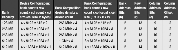
In this section, Intel’s 82955X Memory Controller Hub (MCH) is used as an example to illustrate address mapping schemes in a high-performance, multi-channel, multi-rank memory system. The 82955X MCH contains two memory controllers that can independently control two channels of DDR2 SDRAM devices. Each channel in the 82955X MCH supports up to four ranks of DRAM devices, and Table 13.3 summarizes six possible rank configurations supported by the 82955X MCH. In practical terms, system boards that utilize the 82955X MCH can support one or two memory modules in each channel, and each memory module is composed of one or two identically configured ranks listed in Table 13.3.
The 82955X MCH supports address mapping schemes that are optimized for an open-page memory system. The interesting aspect of the 82955X MCH is that it supports different mapping schemes that are respectively targeted to obtain higher performance or configuration flexibility, and the 82955X MCH can deploy different mapping schemes depending on the organization of the memory modules inserted into the system. Specifically, the 82955X MCH can support the two channels configured with symmetric or asymmetric organizations of memory modules. Moreover, the 82955X MCH uses rank configuration registers to perform address mapping on a rank-by-rank basis. The topics of channel symmetry and per-rank address mapping in the 82955X MCH are examined in detail in the following sections.
Symmetric and Asymmetric Dual Channel Modes
In the case that the two channels are populated with memory modules with symmetrically matched capacities, the 82955X MCH can operate in symmetric dual channel mode. In the symmetric dual channel mode, sequentially consecutive cacheline addresses are mapped to alternating channels so that requests from a streaming request sequence are mapped to both channels concurrently. In the case where the 82955X MCH is configured with different capacities of memory modules in the two channels, the 82955X MCH operates in asymmetric dual channel mode. In the asymmetric dual channel mode, the physical address is mapped from 0 MB to the capacity of channel 0 and then to the full capacity of channel 1. In this manner, requests from a streaming request sequence are mapped to one channel at a time unless the array address space spans both channels.
Figure 13.3 illustrates a symmetric configuration and an asymmetric configuration for the 82955X MCH. The figure shows that in the symmetric configuration, both channel 0 and channel 1 are populated with a single-rank, 512-MB memory module that occupies rank 0 and a single-rank, 256-MB memory module that occupies rank 1. Although the 256-MB memory modules in rank 1 of both channels are not identical in organization, the fact that they are identical in capacity is sufficient for the 82955X MCH to utilize the symmetric dual channel mode. In contrast, the asymmetric configuration example shows that the two channels are populated with memory modules with different capacities and different numbers of ranks. In the asymmetric configuration, the physical address space extends from 0 to 512 MB in channel 0 and then from 512 to 1536 MB in channel 1.

Address Mapping Configuration Registers
The 82955X MCH uses configuration registers to support different address mapping schemes for performance optimization or configuration flexibility. Two types of configuration registers are used in the 82955X MCH to aid it in the task of address mapping: rank address boundary registers and rank architectural registers.
The function of the rank address boundary register is to define the upper address boundaries for a given rank of DRAM devices. There are four rank address boundary registers per channel. In asymmetrical channel model, each register contains the highest addressable location of a single channel of memory. In symmetrical channel mode, cacheline addresses are interleaved between the two channels, and the rank address boundary registers contain the upper address boundaries for a given rank of DRAM devices for both channels of memory. The rank architectural registers identify the size of the row for the DRAM devices inserted into the system. In the 82955X MCH, there are four rank architectural registers per channel, with one register per rank.
Per-Rank Address Mapping Schemes
The address mapping configuration registers are set at system initialization time by the 82955X MCH, and they contain values that reflect the capacity and organization of the DRAM devices in the memory system. With the aid of the rank address boundary configuration registers, the 82955X MCH can unambiguously resolve a physical address location to a given rank of memory. Then, with the aid of the rank architectural registers, the organization of the DRAM devices to the given rank of memory is also known, and the physical address can be further separated into row, bank, and column addresses. That is, the address mapping scheme in the 82955X MCH is generated on a rank-by-rank basis.
Figure 13.4 illustrates the address mapping scheme of 82955X MCH. The figure shows that in single channel or asymmetric dual channel mode, the 82955X MCH maps the three least significant bits of the physical address as the byte offset of the 8-byte-wide memory module. Then, depending on the number of columns on the memory module, the next 9 or 10 bits of the physical address are used to denote the column address field. The bank address then follows the column address, and the most significant address bits are used for the row address.

In the 82955X MCH, the channel address is mapped to different address bit fields, depending on the operating mode of the memory controller. Figure 13.4 does not show the channel address field for the single channel or asymmetric channel mode, since each channel is a contiguous block of memory, and the channel address is mapped to the highest available physical address bit field. However, in symmetric dual channel mode, the cacheline addresses are interleaved between the two channels, and the channel address is mapped to the low range of the address bit fields. Specifically, Figure 13.4 shows that the address mapping schemes shown for the single/asymmetric channel mode and the dual channel symmetric mode are essentially the same, and the only difference between the two sets of address mapping schemes is that the 6th bit in the physical address is used to denote the channel address, and the respective addresses in the dual channel mode are shifted over by 1 bit position to the left.
Quick Summary of Address Mapping in the 82955X MCH
Figure 13.4 serves as a concrete example that illustrates some interesting aspects of address mapping schemes used in contemporary memory controllers. In particular, the address mapping schemes illustrated in Figure 13.4 for the 82955X MCH are classical open-page-optimal address mapping schemes. For example, Figure 13.4 shows that in the single/asymmetric channel mode, the address mapping scheme in the 82955X MCH can be represented as k:l:r:b:n:z, and in the symmetric dual channel mode, the address mapping scheme can be represented as l:r:b:n:k:z. In both cases, the column address fields are mapped to the low address ranges so that spatially adjacent memory address locations can be directed to the same open page. Similarly, in the various address mapping schemes illustrated in Figure 13.4, the 82955X MCH shows that the side effect of granting the end-users the ability to configure the memory system with differently organized memory modules is that rank parallelism to spatially adjacent memory accesses is lost. Although the rank address field is not explicitly illustrated in Figure 13.4, the use of the address boundary registers and per-rank address mapping schemes means that the rank address field is mapped to the high address ranges above the row address field.
Figure 13.4 shows that the 82955X MCH has been cleverly designed so that most of the bit positions are directed to the same address fields regardless of the organization of the memory modules in the memory system. For example, Figure 13.4 shows that physical address bits 16 through 26 are used to denote row addresses 0 through 10 in the single/asymmetric channel mode, regardless of the number and type of memory modules placed in the memory system. In this manner, only a few bit positions will have to be dynamically adjusted depending on the organization of the memory system, and bit positions shown with the grey background in Figure 13.4 are always directed to the same address fields.
Finally, the address mapping scheme in the 82955X MCH means that single threaded streaming applications often cannot take advantage of the parallelism afforded by multiple ranks and the two channels in asymmetric channel mode. Fortunately, multiprocessor and multi-threaded processor systems with concurrently executing contexts can access different regions of memory and may be able to take advantage of the parallelism afforded by the multiple ranks and multiple channels in asymmetric channel mode. However, the amount of achievable parallelism depends on the specific access request sequences and the locations of the data structures accessed by the concurrently executing process contexts.
13.3.6 Bank Address Aliasing (Stride Collision)
One additional issue in the consideration of an address mapping scheme is the problem of bank address aliasing. The problem of bank address aliasing occurs when arrays whose respective sizes are relatively large powers-of-two are accessed concurrently with strided accesses to the same bank. Figure 13.4 shows that in a system that uses 1-GB DDR2 SDRAM memory modules with the 82955X MCH in dual channel mode, the bank address for each access is obtained from physical address bit positions 14 through 16. That is, in this system configuration, all contiguously allocated arrays that are aligned on address boundaries that are integer multiples of 217 bytes from each other would have array elements that map to identical banks for all corresponding array elements.
For example, the task of array summation, where the array elements of arrays A and B are added together and then stored into array C, requires that the corresponding elements of A, B, and C be accessed concurrently. In the case where arrays A, B, and C are contiguously allocated by the system and mapped to integer multiples of 128-kB address boundaries from each other, then array elements A[i], B[i], and C[i], would be mapped to different rows within the same bank for all valid array indices i, resulting in multiple bank conflicts for each step of the array summation process in the system described above.
In general, the bank address aliasing problem can be alleviated by several different methods. One method that can alleviate the bank address aliasing problem is the conscientious application of padding or offsets to large arrays so that bank conflicts are not generated throughout concurrent array accesses to those large arrays.10 A second method that can alleviate the bank address aliasing problem is the conscientious design of a memory management unit that can purposefully allocate large arrays to non-contiguous pages in the physical address space. In this manner, the chance of a bank conflict changes from a guaranteed event that occurs for every single access to the array to a probabilistic event that depends on the number of banks and ranks in the memory system. Finally, improved address mapping schemes have been proposed to alleviate the bank address aliasing problem, and they are described in the following section.
Hardware Solution to the Address Aliasing Problem
The bank address aliasing problem has been investigated by Lin et al. [2001] and Zhang et al. [2000]. The schemes proposed by Lin and Zhang are similar to schemes applied to different memory systems. The basic idea of taking the row address and bitwise XOR’ed with the bank address to generate new bank addresses that are not aligned for concurrent accesses to large arrays is common to both designs. However, the generous rank and bank parallelism in the fully configured Direct RDRAM memory system allowed Lin to create a 1:1 mapping that permutes the available number of banks through the entire address space in the system configuration examined. In contrast, Zhang illustrated a more modest memory system where the page index was larger than the bank index. The mapping scheme described by Zhang is shown in Figure 13.5. Figure 13.5 shows that the problem for the scheme described by Zhang is that there are relatively few banks in contemporary SDRAM and DDRx SDRAM memory systems, and for a DRAM memory system with 2b banks, there are only 2b possible permutations in a 1:1 mapping that maps a physical address to the memory address. In the bank address permutation scheme for the conventional SDRAM-type memory system proposed by Zhang, the address aliasing problem is simply shifted to a larger granularity. That is, without the bank permutation scheme illustrated in Figure 13.5, arrays aligned on address boundaries of 2(b+p) bytes would suffer a bank conflict on every pair of concurrent array accesses. The implementation of the bank permutation scheme means that arrays aligned on address boundaries of 2(b+p) bytes no longer suffer from the same address aliasing problem, but arrays that are aligned on address boundaries of 2(b+p+b) bytes continue to suffer a bank conflict on every pair of concurrent array accesses. Essentially, there are not enough banks to rotate through the entire address space in a contemporary memory system to completely avoid the memory address aliasing problem.

FIGURE 13.5 Address mapping scheme proposed by Zhang et al. [2000].
13.4 Performance Optimization
The performance characteristic of a modern DRAM memory controller depends on implementation-specific DRAM command and memory transaction ordering policies. A DRAM controller can be designed to minimize complexity without regard to performance or designed to extract the maximum performance from the memory system by implementing aggressive DRAM command and memory transaction ordering policies. DRAM command and transaction ordering policies have been studied by Briggs et al. [2002], Cuppu et al. [1999], Hur and Lin [2004], McKee et al. [1996], Lin et al. [2001], and Rixner et al. [2000]. In studies performed by Briggs et al., Cuppu et al., McKee et al., Lin et al., and Rixner et al., various DRAM-centric scheduling schemes are examined. In the study performed by Hur et al., the observation is noted that the ideal DRAM scheduling algorithm depends not only on the optimality of scheduling to the DRAM memory system, but also on the requirement of the application. In particular, the integration of DRAM memory controllers with the processor core onto the same silicon die means that the processor core can interact directly with the memory controller and provide direct feedback to select the optimal DRAM command scheduling algorithm.
The design of a high-performance DRAM memory controller is further complicated by the emergence of modern, high-performance, multi-threaded processors and multi-core processors. While the use of multi-threading has been promoted as a way to hide the effects of memory-access latency in modern computer systems, the net effect of multi-threaded and multi-core processors on a DRAM memory system is that the intermixed memory request stream from the multiple threaded contexts to the DRAM memory system disrupts the row locality of the request pattern and increases bank conflicts [Lin et al. 2001]. As a result, an optimal DRAM controller design not only has to account for the idiosyncrasies of specific DRAM memory systems, application-specific requirements, but also the type and number of processing elements in the system.
The large number of design factors that a design engineer must consider underlines the complexity of a high-performance DRAM memory controller. Fortunately, some basic strategies exist in common for the design of high-performance DRAM memory controllers. Specifically, the strategies of bank-centric organization, write caching, and seniors first are common to many high-performance DRAM controllers, while specific adaptive arbitration algorithms are unique to specific DRAM controllers and systems.
13.4.1 Write Caching
One strategy deployed in many modern DRAM controllers is the strategy of write caching. The basic idea for write caching is that write requests are typically non-critical in terms of latency, but read requests are typically critical in terms of latency. As a result, it is typically desirable to defer write requests and allow read requests to proceed ahead of write requests, as long as the memory ordering model of the system supports this optimization and the functional correctness of programs is not violated. Furthermore, DRAM devices are typically poorly designed to support back-to-back read and write requests. In particular, a column read command that occurs immediately after a column write command typically incurs a large penalty in the data bus turnaround time in conventional DDRx SDRAM devices due to the fact that the column read command must await the availability of the internal datapath of the DRAM device that is shared between read and write commands.
Figure 13.6 repeats the illustration of a column read command that follows a write command and shows that, due to the differences in the direction of data flow between read and write commands, significant overheads exist when column read and write commands are pipelined back to back. The strategy of write caching allows read requests that may be critical to application performance to proceed ahead of write requests, and the write caching strategy can also reduce read-write overheads when combined with a strategy to burst multiple write requests to the memory system consecutively. One memory controller that utilizes the write caching strategy is Intel’s i8870 system controller which can buffer upwards of 8 kB of write data to prioritize read requests over write requests. However, in systems that implement write caching, significant overhead in terms of latency or hardware complexity may exist due to the fact that the address of all pending read requests must be checked against the address of cached writes, and the memory controller must provide the consistency guarantee to ensure the correctness of memoryaccess ordering.

13.4.2 Request Queue Organizations
To control the flow of data between the DRAM memory controller and DRAM devices, memory transactions are translated into sequences of DRAM commands in modern DRAM memory controllers. To facilitate the pipelined execution of these DRAM commands, the DRAM commands may be placed into a single queue or multiple queues. With the DRAM commands organized in the request queuing structure, the DRAM memory controller can then prioritize DRAM commands based on many different factors, including, but not limited to, the priority of the request, the availability of resources to a given request, the bank address of the request, the age of the request, or the access history of the agent that made the request.
One organization that can facilitate the pipelined execution of DRAM commands in a high-performance DRAM memory controller is the per-bank queuing organization.11 In the per-bank queuing structure, memory transaction requests, assumed to be of equal priority, are sorted and directed to different queues on a bank-by-bank basis. Figure 13.7 shows one organization of a set of request queues organized on a per-bank basis. In the organization illustrated in Figure 13.7, memory transaction requests are translated into memory addresses and directed into different request queues based on their respective bank addresses. In an open-page memory controller with request queues organized comparably to Figure 13.7, multiple column commands can be issued from a given request queue to a given bank if the column access commands are directed to the same open row. In the case where a given request queue has exhausted all pending requests to the same open row and all other pending requests in the queue are addressed to different rows, the request queue can then issue a precharge command and allow the next bank to issue commands into the memory system.12
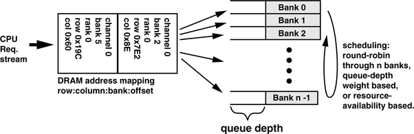
Figure 13.7 shows that one way to schedule requests from the per-bank queuing structure is to rotate the scheduling priority in a round-robin fashion from bank to bank. The round-robin, bank-rotation command scheduling scheme can effectively hide DRAM bank conflict overhead to a given bank if there are sufficient numbers of pending requests to other banks that can be processed before the scheduling priority rotates back to the same bank. In a close-page memory controller, the round-robin bank-rotation scheme maximizes the temporal distance between requests to any given bank without sophisticated logic circuits to resolve against starvation. However, the round-robin scheme may not always produce optimal scheduling, particularly, for open-page memory controllers. In open-page memory controllers, the address mapping scheme maps spatially adjacent cachelines to open rows, and multiple requests to an open row may be pending in a given queue. As a result, a weight-based priority scheduling scheme, where the queue with the largest number of pending requests, is prioritized ahead of other queues with fewer pending requests, may be more optimal than a strictly round-robin priority scheduling scheme.13
The per-bank queue organization may be favored in large memory systems where high request rates are directed to relatively few banks. In memory systems where there are relatively lower access rates to a large number of banks in the system, dedicated per-banks queues are less efficient in organizing requests. In these memory systems, the queue structure may be more optimally organized as a pool of general-purpose queue entries where each queue entry can be directed to different banks as needed.
13.4.3 Refresh Management
One issue that all modern DRAM controllers must deal with to ensure the integrity of data stored in DRAM devices is the refresh function. In the case where a modern memory system is inactive for a short period of time, all DRAM devices can make use of a DRAM device controlled self-refresh mode, where the DRAM memory controller can be temporarily powered down and placed into a sleep state while the DRAM device controls its own refresh function. However, the entry into and exit out of the self-refresh mode is typically performed under the explicit control of the DRAM memory controller, and the self-refresh action is not engaged in during normal operations in most modern DRAM devices.
One exception to the explicit management of the refresh function by the memory controller can be found in some pseudo-static DRAM devices such as MobileRAM, where temperature-compensated self-refresh is used as part of the normal operating mode to minimize refresh power consumption. Moreover, the hidden self-refresh removes the complexity of refresh control from the memory controller and contributes to the illusion of the MobileRAM DRAM device as a pseudo-static memory device. The timing and interval of the DRAM refresh action in these devices are hidden from the memory controller. Therefore, in the case where a memory request from the memory controller collides with the hidden refresh action, the pseudo-static DRAM device asserts a wait signal to inform the memory controller that the data return from the pseudo-static DRAM device will be delayed until after the self-refresh action within the pseudo-static DRAM device is completed and the wait signal is deasserted by the pseudo-static DRAM device. However, a wait signal from the pseudo-static DRAM device that can delay state transition in the memory controller effectively introduces a slow signal path into the memory controller and effectively limits the operating frequency of the memory controller. Consequently, the explicit wait state signal that enables the hidden self-refresh function in normal operating mode is only used in relatively low-frequency, pseudo-static DRAM-based memory systems designed for battery-operated mobile platforms, and the refresh function in DRAM devices targeted for high-frequency DRAM memory systems remains under the purview of the DRAM memory controller.
To ensure the integrity of data stored in DRAM devices, each DRAM row that contains valid data must be refreshed at least once per refresh period, typically 32 or 64 ms in duration.14 In terms of a DRAM device that requires 8192 refresh commands every refresh period, mathematics dictate that an all-banks-concurrent refresh command must be issued to the DRAM device once every 7.8 μs for the device with a 64-ms period requirement. Fortunately, DRAM refresh commands can be deferred for short periods of time to allow latency-critical memory read requests to proceed ahead. Consequently, the DRAM controller need not adhere to a strict requirement of having to send an all-banks-concurrent refresh command to the DRAM device every 7.8 μs. To take advantage of the fact that refresh commands can be deferred within a reasonable timing window, Figure 13.8 shows an organization of the queuing structure where the microprocessor request stream is separated into read and write request queues and the request commands are placed into the refresh queue at a constant rate of one refresh command every 7.8 μs. In the structure illustrated in Figure 13.8, each refresh request is attributed with a count that denotes the number of cycles that the request has been deferred. In this manner, in the case that the refresh request is below a preset deferral threshold, all read and write requests will have priority over the refresh request.15 In the case where the system is idle with no other pending read or write requests, the refresh request can then be sent to the DRAM devices. In the case where the system is filled with pending read and write requests but a DRAM refresh request has nearly exceeded the maximum deferral time, that DRAM refresh request will then receive the highest scheduling priority to ensure that the refresh request occurs within the required time period to ensure data integrity in the memory system.

One feature under consideration that could further increase the complexity of future DRAM memory controllers is the functionality of per-bank refresh. Table 13.4 illustrates that tRFC, the refresh cycle time, is increasing with each generation of higher density DRAM devices, and the bandwidth overhead of the refresh functionality grows proportionally.16 One proposal to minimize the bandwidth impact of DRAM refresh is to replace or supplement the all-banks-concurrent refresh command with separate refresh commands that refresh one row in one bank at a time as opposed to refreshing one row in all banks within a rank of DRAM devices concurrently.17

The performance benefit of the separate per-bank refresh command can be easily computed since each per-bank refresh command need only respect the tRC row cycle time constraint rather than the tRFC refresh cycle time constraint. However, one caveat of the per-bank refresh command proposal is that the fine-grained control of the refresh function on a per-bank basis means that the complexity of the DRAM memory controller must increase proportionally to deal with separate refresh requests to each bank, and the queueing structure required may be far more complex than the sample queuing structure illustrated in Figure 13.7. Finally, the all-banks-concurrent refresh command also serves as a time period where the DRAM device can perform housekeeping duties such as signal recalibration between DRAM devices and the memory controller. Without the all-banks-concurrent refresh command, DRAM devices would lose the guaranteed time period where circuits within the DRAM devices are active, but the interface of the DRAM devices are idle to perform these types of housekeeping duties.
13.4.4 Agent-Centric Request Queuing Organization
In previous sections, techniques to maximize bandwidth utilization and decrease effective read latency were examined. However, one issue that was left out of previous discussions is that regardless of the performance techniques deployed, an overriding consideration in the design of a modern DRAM memory controller is one of fairness. That is, in any transaction request reordering mechanism, anti-starvation safeguards must exist to ensure that no request can be deferred for an indefinite period of time. The anti-starvation safeguards are particularly important in the context of multiple agents that share use of the same memory system. In particular, the issues of fairness and performance optimization for multiple agents with drastically different request rates and address sequences must be carefully traded off against each other. For example, a microprocessor running a typical application may require relatively low bandwidth, but read requests from the processor must be considered as latency critical. In contrast, a graphics processor that is connected to the same memory system may require a large amount of guaranteed bandwidth, but individual memory transaction requests from the graphics processor may be deferred in favor of requests from the microprocessor. Finally, memory transaction requests from relatively low-bandwidth and low-priority I/O devices may be deferred, but these requests cannot be deferred for an indefinite period of time so as to cause starvation for the I/O devices. That is, in the context of multiple agents that share a common memory system, better performance may be measured in terms of achieving an equitable balance in the usage of the memory system rather than obtaining the absolute maximum bandwidth from the DRAM devices.
The conflicting requirements of fairness and performance are important considerations that must be accounted for by the DRAM memory controller’s scheduling mechanism. Fortunately, the scheduling mechanism used to deal with the DRAM device refresh requirement can be broadly extended to deal with a broad range of agents that require low latency or guaranteed bandwidth. That is, DRAM refresh commands can be considered as a sequence of requests from an agent that requires some amount of guaranteed bandwidth from the DRAM memory system. This agent, along with a number of other agents that require differing amounts of guaranteed bandwidth, must share the memory system with other agents that have no fixed requirements in terms of bandwidth, but must have low average access latency.
Figure 13.9 shows an organization of the queuing structure where the memory controller selects between requests from low-latency agents and guaranteed bandwidth agents. Figure 13.9 shows that requests from low-bandwidth and guaranteed bandwidth agents are directed to a two-level queuing structure, where requests are first sent to a pending queue and then moved to a scheduling queue under respective rate-controlled conditions. The rate controls ensure that the non-latency critical request agents cannot saturate the memory system with requests at the expense of other agents. In the queuing structure illustrated in Figure 13.9, requests from the low-latency agents are typically scheduled with the highest priority, except when the scheduling queue for the guaranteed bandwidth agents are full. To ensure that the bandwidth guarantees are met, the scheduling priority must favor the guaranteed bandwidth agents in the case where the shared scheduling queue for the guaranteed bandwidth agents is full.
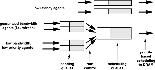
In the previous section, DRAM-centric request scheduling algorithms are examined in the context of obtaining the highest performance from the DRAM memory system, given that all requests are equal in importance and that requests can be freely reordered for better performance. However, in a system where multiple agents must share the use of the memory system, not all requests from different agents are equal in importance. As a result, to obtain better performance in the system as a whole, both DRAM-centric and agent-centric algorithms must be considered. Figure 13.9 thus illustrates a two-level scheduling algorithm to ensure fairness and system throughput.
13.4.5 Feedback-Directed Scheduling
In modern computer systems, memory access is performed by the memory controller on behalf of processors or intelligent I/O devices. Memory-access requests are typically encapsulated in the form of transaction requests that contain the type, address, and data for the request in the case of write requests. However, in the majority of systems, transaction requests typically do not contain information to allow a memory controller to prioritize the transactions based on the specific requirements of the workload. Rather, memory controllers typically rely on the type, the access history, the requesting agent, and the state of the memory system to prioritize and schedule the memory transactions. In one recent study performed by Hur and Lin [2004], the use of a history-based arbiter that selects among different scheduling policies is examined in detail. In this study, the memory-access request history is used to select from different prioritization policies dynamically, and speedups between 5 and 60% are observed on some benchmarks.
The exploration of a history-based DRAM transaction and command scheduling algorithm by Hur and Lin is enabled by the use of a processor with an integrated DRAM controller, the IBM POWER5. The trend in the integration of memory controllers and processors means that the memory controllers will gain access to transaction scheduling information that they could not access as stand alone controllers.
As more processors are designed with integrated DRAM memory controllers, these processors can communicate directly with the DRAM memory controllers and schedule DRAM commands based not only on the availability of resources within the DRAM memory system, but also on the DRAM command-access history. In particular, as multi-threaded and multi-core processors are integrated with DRAM memory controllers, these DRAM memory controllers not only have to be aware of the availability of resources within the DRAM memory system, but they must also be aware of the state and access history of the respective threaded contexts on the processor in order to achieve the highest performance possible.
13.5 Summary
An analogy that may be made for the transaction queuing mechanism of a modern, high-performance DRAM memory controller is one that compares the transaction queuing mechanism of a high-performance DRAM controller to the instruction Reorder Buffer (ROB) of high-performance microprocessors that dynamically convert assembly instructions into internal microoperations that the processor executes out of order. In the ROB, the microprocessor accepts as input a sequence of assembly instructions that it converts to microoperations. In the transaction queue of the memory controller, the transaction queue accepts read and write requests that it must convert to DRAM commands that the memory controller then attempts to execute. Similar to the microoperations in the ROB, DRAM commands can be scheduled subject to the ordering constraints of the transaction requests and availability of the resources.
1In some DRAM devices that strive to be SRAM-like, the row-activation command and the column-access command are coupled into a single read or write command. These devices do not support the open-page row-buffer-management policies. Typically, these DRAM devices are designed as low-latency, random-access memory and used in speciality embedded systems.
2That is, assuming that the probability of having to wait for tRAS of the previous row activation is equal in open-page and close-page memory systems. If the probability of occurrence is the same, then the latency overheads are the same and can be ignored.
3Or increase to a significantly higher multiple of tRCD.
4Or decrease to a small fraction of tRCD.
5Commodity DRAM devices such as DDR2 SDRAM devices consume approximately the same amount of power in active standby mode as it does in precharge standby mode, so power optimality of the paging policy is device-dependent.
6Fully Buffered DIMM memory systems present an interesting path to an unconventional system architecture that the Impulse memory controller or an Impulse-like memory controller may be able to take advantage of. That is, with multiple memory controllers controlling multiple, independent channels of Fully Buffered DIMMs, some channels may be designated for general-purpose access as in a conventional system architecture, while other channels may be used as high bandwidth, application-controlled, direct-access memory systems.
7The exploration of parallelism in the memory system is an attempt to extract maximum performance. For low-power targeted systems, different criteria may be needed to optimize the address mapping scheme.
8Overhead-free scheduling of consecutive column accesses to different banks of a given rank of DRAM devices has long been the most efficient way to schedule memory commands. However, constraints such as burst chop in DDR3 SDRAM devices and tFAW constraints in 8-bank DDRx SDRAM devices is now shifting the overhead distribution. Consequently, rank parallelism may be more favorable than bank parallelism in future DDRx SDRAM memory systems.
9Again, assume a uniform memory system where all channels have identical configurations in terms of banks, ranks, rows, and columns.
10A simple offset insertion increased STREAM Triad bandwidth by 25% in a test system with an Intel i875P system controller.
11The per-bank request queuing construct is an abstract construct. Memory controllers can utilize a unified queue with sophisticated hardware to perform the transaction reordering and bank rotation described herein, albeit with greater difficulty.
12The bank-centric organization assumes that all requests from different agents are of equal priority and access rates from different agents are comparable. In practical terms, additional safeguards must be put in place to prevent the scenario where a constant stream of requests to an open row starves other requests to different rows. In some controllers, a limit is placed on the maximum number of consecutive column commands that can be scheduled to an open row before the open row is closed to prevent starvation and to ensure some degree of fairness to requests made to different rows of the same bank.
13Weight-based schemes must also be constrained by age considerations to prevent starvation.
14Some DRAM devices contain additional registers to define the ranges of rows that need to be refreshed. In these devices, the refresh action can be ignored for certain rows that do not contain valid data.
15The maximum refresh request deferral time is defined in the device data sheet for DRAM devices. In modern DRAM devices such as DDR2 SDRAM devices, the period DRAM refresh command can be deferred for as long a 97.8-μs refresh command intervals.
16There are more than 8192 rows in higher density DDR2 SDRAM devices, but the number of refresh commands per 64-ms time period remains constant. For example, the 4-Gbit DDR2 device must refresh 8 rows of data with each refresh command.
17The refresh command is a relatively energy-intensive operation. The instantaneous power draw of large, multi-rank memory systems, where all ranks are refreshed concurrently with a single refresh command, could significantly increase the peak power consumption profile of the memory system. To limit the peak power consumption profile, some DRAM memory controllers are designed to refresh each rank of DRAM devices separately and scheduled some time apart from each other.