
Overview of DRAMs
DRAM is the “computer memory” that you order through the mail or purchase at the store. It is what you put more of into your computer as an upgrade to improve the computer’s performance. It appears in most computers in the form shown in Figure 7.1—the ubiquitous memory module, a small computer board (a printed circuit board, or PCB) that has a handful of chips attached to it. The eight black rectangles on the pictured module are the DRAM chips: plastic packages, each of which encloses a DRAM die (a very thin, fragile piece of silicon).

FIGURE 7.1 A memory module. A memory module, or DIMM (dual in-line memory module), is a circuit board with a handful of DRAM chips and associated circuitry attached to it.
Figure 7.2 illustrates DRAM’s place in a typical PC. An individual DRAM device typically connects indirectly to a CPU (i.e., a microprocessor) through a memory controller. In PC systems, the memory controller is part of the north-bridge chipset that handles potentially multiple microprocessors, the graphics co-processor, communication to the south-bridge chipset (which, in turn, handles all of the system’s I/O functions), as well as the interface to the DRAM system. Though still often referred to as “chipsets” these days, the north- and south-bridge chipsets are no longer sets of chips; they are usually implemented as single chips, and in some systems the functions of both are merged into a single die.

FIGURE 7.2 A typical PC organization. The DRAM subsystem is one part of a relatively complex whole. This figure illustrates a two-way multi-processor, with each processor having its own dedicated secondary cache. The parts most relevant to this report are shaded in darker grey: the CPU, the memory controller, and the individual DRAMs.
Because DRAM is usually an external device by definition, its use, design, and analysis must consider effects of implementation that are often ignored in the use, design, and analysis of on-chip memories such as SRAM caches and scratch-pads. Issues that a designer must consider include the following:
Failure to consider these issues when designing a DRAM system is guaranteed to result in a sub-optimal, and quite probably non-functional, design. Thus, much of this section of the book deals with low-level implementation issues that were not covered in the previous section on caches.
7.1 DRAM Basics: Internals, Operation
A random-access memory (RAM) that uses a single transistor-capacitor pair for each bit is called a dynamic random-access memory or DRAm. Figure 7.3 shows, in the bottom right corner, the circuit for the storage cell in a DRAm. This circuit is dynamic because the capacitors storing electrons are not perfect devices, and their eventual leakage requires that, to retain information stored there, each capacitor in the DRAM must be periodically refreshed (i.e., read and rewritten).

FIGURE 7.3 Basic organization of DRAM internals. The DRAM memory array is a grid of storage cells, where one bit of data is stored at each intersection of a row and a column.
Each DRAM die contains one or more memory arrays, rectangular grids of storage cells with each cell holding one bit of data. Because the arrays are rectangular grids, it is useful to think of them in terms associated with typical grid-like structures. A good example is a Manhattan-like street layout with avenues running north–south and streets running east–west. When one wants to specify a rendezvous location in such a city, one simply designates the intersection of a street and an avenue, and the location is specified without ambiguity. Memory arrays are organized just like this, except where Manhattan is organized into streets and avenues, memory arrays are organized into rows and columns. A DRAM chip’s memory array with the rows and columns indicated is pictured in Figure 7.3. By identifying the intersection of a row and a column (by specifying a row address and a column address to the DRAM), a memory controller can access an individual storage cell inside a DRAM chip so as to read or write the data held there.
One way to characterize DRAMs is by the number of memory arrays inside them. Memory arrays within a memory chip can work in several different ways. They can act in unison, they can act completely independently, or they can act in a manner that is somewhere in between the other two. If the memory arrays are designed to act in unison, they operate as a unit, and the memory chip typically transmits or receives a number of bits equal to the number of arrays each time the memory controller accesses the DRAm. For example, in a simple organization, a x4 DRAM (pronounced “by four”) indicates that the DRAM has at least four memory arrays and that a column width is 4 bits (each column read or write transmits 4 bits of data). In a x4 DRAM part, four arrays each read 1 data bit in unison, and the part sends out 4 bits of data each time the memory controller makes a column read request. Likewise, a x8 DRAM indicates that the DRAM has at least eight memory arrays and that a column width is 8 bits. Figure 7.4 illustrates the internal organization of x2, x4, and x8 DRAMs. In the past two decades, wider output DRAMs have appeared, and x16 and x32 parts are now common, used primarily in high-performance applications.
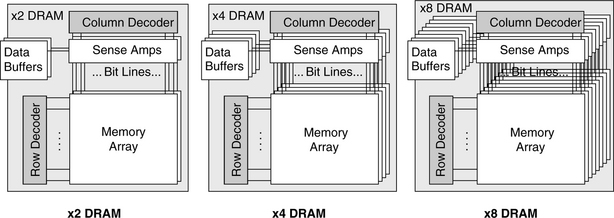
FIGURE 7.4 Logical organization of wide data-out DRAMs. If the DRAM outputs more than one bit at a time, the internal organization is that of multiple arrays, each of which provides one bit toward the aggregate data output.
Note that each of the DRAM illustrations in Figure 7.4 represents multiple arrays but a single bank. Each set of memory arrays that operates independently of other sets is referred to as a bank, not an array. Each bank is independent in that, with only a few restrictions, it can be activated, precharged, read out, etc. at the same time that other banks (on the same DRAM device or on other DRAM devices) are being activated, precharged, etc. The use of multiple independent banks of memory has been a common practice in computer design since DRAMs were invented. In particular, interleaving multiple memory banks has been a popular method used to achieve high-bandwidth memory busses using low-bandwidth devices. In an interleaved memory system, the data bus uses a frequency that is faster than any one DRAM bank can support; the control circuitry toggles back and forth between multiple banks to achieve this data rate. For example, if a DRAM bank can produce a new chunk of data every 10 ns, one can toggle back and forth between two banks to produce a new chunk every 5 ns, or round-robin between four banks to produce a new chunk every 2.5 ns, thereby effectively doubling or quadrupling the data rate achievable by any one bank. This technique goes back at least to the mid-1960s, where it was used in two of the highest performance (and, as it turns out, best documented) computers of the day: the IBM System/360 Model 91 [Anderson et al. 1967] and Seymour Cray’s Control Data 6600 [Thornton 1970].
Because a system can have multiple DIMMs, each of which can be thought of as an independent bank, and the DRAM devices on each DIMM can implement internally multiple independent banks, the word “rank” was introduced to distinguish DIMM-level independent operation versus internal-bank-level independent operation. Figure 7.5 illustrates the various levels of organization in a modern DRAM system. A system is composed of potentially many independent DIMMs. Each DIMM may contain one or more independent ranks. Each rank is a set of DRAM devices that operate in unison, and internally each of these DRAM devices implements one or more independent banks. Finally, each bank is composed of slaved memory arrays, where the number of arrays is equal to the data width of the DRAM part (i.e., a x4 part has four slaved arrays per bank). Having concurrency at the rank and bank levels provides bandwidth through the ability to pipeline requests. Having multiple DRAMs acting in unison at the rank level and multiple arrays acting in unison at the bank level provides bandwidth in the form of parallel access.

FIGURE 7.5 DIMMs, ranks, banks, and arrays. A system has potentially many DIMMs, each of which may contain one or more ranks. Each rank is a set of ganged DRAM devices, each of which has potentially many banks. Each bank has potentially many constituent arrays, depending on the part’s data width.
The busses in a JEDEC-style organization are classified by their function and organization into data, address, control, and chip-select busses. An example arrangement is shown in Figure 7.6, which depicts a memory controller connected to two memory modules. The data bus that transmits data to and from the DRAMs is relatively wide. It is often 64 bits wide, and it can be much wider in high-performance systems. A dedicated address bus carries row and column addresses to the DRAMs, and its width grows with the physical storage on a DRAM device (typical widths today are about 15 bits). A control bus is composed of the row and column strobes,1 output enable, clock, clock enable, and other related signals. These signals are similar to the address-bus signals in that they all connect from the memory controller to every DRAM in the system. Finally, there is a chip-select network that connects from the memory controller to every DRAM in a rank (a separately addressable set of DRAMs). For example, a memory module can contain two ranks of DRAM devices; for every DIMM in the system, there can be two separate chip-select networks, and thus, the size of the chip-select “bus” scales with the maximum amount of physical memory in the system.

FIGURE 7.6 JEDEC-style memory bus organization. The figure shows a system of a memory controller and two memory modules with a 16-bit data bus and an 8-bit address and command bus.
This last bus, the chip-select bus, is essential in a JEDEC-style memory system, as it enables the intended recipient of a memory request. A value is asserted on the chip-select bus at the time of a request (e.g., read or write). The chip-select bus contains a separate wire for every rank of DRAM in the system. The chip-select signal passes over a wire unique to each small set of DRAMs and enables or disables the DRAMs in that rank so that they, respectively, either handle the request currently on the bus or ignore the request currently on the bus. Thus, only the DRAMs to which the request is directed handle the request. Even though all DRAMs in the system are connected to the same address and control busses and could, in theory, all respond to the same request at the same time, the chip-select bus prevents this from happening.
Figure 7.7 focuses attention on the microprocessor, memory controller, and DRAM device and illustrates the steps involved in a DRAM request. As mentioned previously, a DRAM device connects indirectly to a microprocessor through a memory controller; the microprocessor connects to the memory controller through some form of network (bus, point-to-point, crossbar, etc.); and the memory controller connects to the DRAM through another network (bus, point-to-point, etc). The memory controller acts as a liaison between the microprocessor and DRAM so that the microprocessor does not need to know the details of the DRAM’s operation. The microprocessor presents requests to the memory controller that the memory controller satisfies. The microprocessor connects to potentially many memory controllers at once; alternatively, many microprocessors could be connected to the same memory controller. The simplest case (a uniprocessor system) is illustrated in the figure. The memory controller connects to potentially many DRAM devices at once. In particular, DIMMs are the most common physical form in which consumers purchase DRAM, and these are small PCBs with a handful of DRAM devices on each. A memory controller usually connects to at least one DIMM and, therefore, multiple DRAM devices at once.

FIGURE 7.7 System organization and the steps of a DRAM read. Reading data from a DRAM is not as simple as an SRAM, and at several of the stages the request can be stalled.
Figure 7.7 also illustrates the steps of a typical DRAM read operation. After ordering and queueing requests, the microprocessor sends a given request to the memory controller. Once the request arrives at the memory controller, it is queued until the DRAM is ready and all previous and/or higher priority requests have been handled. The memory controller’s interface to the DRAM is relatively complex (compared to that of an SRAM, for instance); the row-address strobe (RAS) and column-address strobe (CAS) components are shown in detail in Figure 7.8. Recall from Figure 7.3 that the capacitor lies at the intersection of a wordline and a bitline; it is connected to the bitline through a transistor controlled by the wordline. A transistor is, among other things, a switch, and when the voltage on a wordline goes high, all of the transistors attached to that wordline become closed switches (turned on), connecting their respective capacitors to the associated bitlines. The capacitors at each intersection of wordline and bitline are extremely small and hold a number of electrons that are miniuscule relative to the physical characteristics of those bitlines. Therefore, special circuits called sense amplifiers are used to detect the values stored on the capacitors when those capacitors become connected to their associated bitlines. The sense amplifiers first precharge the bitlines to a voltage level that is halfway between logic level 0 and logic level 1. When the capacitors are later connected to the bitlines through the transistors, the capacitors change the voltage levels on those bitlines very slightly. The sense amplifiers detect the minute changes and pull the bitline voltages all the way to logic level 0 or 1. Bringing the voltage on the bitlines to fully high or fully low, as opposed to the precharged state between high and low, actually recharges the capacitors as long as the transistors remain on.

FIGURE 7.8 The multi-phase DRAM-access protocol. The row access drives a DRAM page onto the bitlines to be sensed by the sense amps. The column address drives a subset of the DRAM page onto the bus (e.g., 4 bits).
Returning to the steps in handling the read request. The memory controller must decompose the provided data address into components that identify the appropriate rank within the memory system, the bank within that rank, and the row and column inside the identified bank. The components identifying the row and column are called the row address and the column address. The bank identifier is typically one or more address bits. The rank number ends up causing a chip-select signal to be sent out over a single one of the separate chip-select lines.
Once the rank, bank, and row are identified, the bitlines in the appropriate bank must be precharged (set to a logic level halfway between 0 and 1). Once the appropriate bank has been precharged, the second step is to activate the appropriate row inside the identified rank and bank by setting the chip-select signal to activate the set of DRAMs comprising the desired bank, sending the row address and bank identifier over the address bus, and signaling the DRAM’s ![]() pin (row-address strobe—the bar indicates that the signal is active when it is low). This tells the DRAM to send an entire row of data (thousands of bits) into the DRAM’s sense amplifiers (circuits that detect and amplify the tiny logic signals represented by the electric charges in the row’s storage cells). This typically takes a few tens of nanoseconds, and the step may have already been done (the row or page could already be open or activated, meaning that the sense amps might already have valid data in them).
pin (row-address strobe—the bar indicates that the signal is active when it is low). This tells the DRAM to send an entire row of data (thousands of bits) into the DRAM’s sense amplifiers (circuits that detect and amplify the tiny logic signals represented by the electric charges in the row’s storage cells). This typically takes a few tens of nanoseconds, and the step may have already been done (the row or page could already be open or activated, meaning that the sense amps might already have valid data in them).
Once the sense amps have recovered the values, and the bitlines are pulled to the appropriate logic levels, the memory controller performs the last step, which is to read the column (column being the name given to the data subset of the row that is desired), by setting the chip-select signal to activate the set of DRAMs comprising the desired bank,2 sending the column address and bank identifier over the address bus, and signaling the DRAM’s ![]() pin (column-address strobe—like
pin (column-address strobe—like ![]() , the bar indicates that it is active when low). This causes only a few select bits3 in the sense amplifiers to be connected to the output drivers, where they will be driven onto the data bus. Reading the column data takes on the order of tens of nanoseconds. When the memory controller receives the data, it forwards the data to the microprocessor.
, the bar indicates that it is active when low). This causes only a few select bits3 in the sense amplifiers to be connected to the output drivers, where they will be driven onto the data bus. Reading the column data takes on the order of tens of nanoseconds. When the memory controller receives the data, it forwards the data to the microprocessor.
The process of transmitting the address in two different steps (i.e., separately transmitted row and column addresses) is unlike that of SRAMs. Initially, DRAMs had minimal I/O pin counts because the manufacturing cost was dominated by the number of I/O pins in the package. This desire to limit I/O pins has had a long-term effect on DRAM architecture; the address pins for most DRAMs are still multiplexed, meaning that two different portions of a data address are sent over the same pins at different times, as opposed to using more address pins and sending the entire address at once.
Most computer systems have a special signal that acts much like a heartbeat and is called the clock. A clock transmits a continuous signal with regular intervals of “high” and “low” values. It is usually illustrated as a square wave or semi-square wave with each period identical to the next, as shown in Figure 7.9. The upward portion of the square wave is called the positive or rising edge of the clock, and the downward portion of the square wave is called the negative or falling edge of the clock. The primary clock in a computer system is called the system clock or global clock, and it typically resides on the motherboard (the PCB that contains the microprocessor and memory bus). The system clock drives the microprocessor and memory controller and many of the associated peripheral devices directly. If the clock drives the DRAMs directly, the DRAMs are called synchronous DRAMs. If the clock does not drive the DRAMs directly, the DRAMs are called asynchronous DRAMs. In a synchronous DRAM, steps internal to the DRAM happen in time with one or more edges of this clock. In an asynchronous DRAM, operative steps internal to the DRAM happen when the memory controller commands the DRAM to act, and those commands typically happen in time with one or more edges of the system clock.

7.2 Evolution of the DRAM Architecture
In the 1980s and 1990s, the conventional DRAM interface started to become a performance bottleneck in high-performance as well as desktop systems. The improvement in the speed and performance of microprocessors was significantly outpacing the improvement in speed and performance of DRAM chips. As a consequence, the DRAM interface began to evolve, and a number of revolutionary proposals [Przybylski 1996] were made as well. In most cases, what was considered evolutionary or revolutionary was the proposed interface (the mechanism by which the microprocessor accesses the DRAM). The DRAM core (i.e., what is pictured in Figure 7.3) remains essentially unchanged.
Figure 7.10 shows the evolution of the basic DRAM architecture from clocked to the conventional asynchronous to fast page mode (FPM) to extended data-out (EDO) to burst-mode EDO (BEDO) to synchronous (SDRAM). The figure shows each as a stylized DRAM in terms of the memory array, the sense amplifiers, and the column multiplexer (as well as additional components if appropriate).

FIGURE 7.10 Evolution of the DRAM architecture. To the original DRAM design, composed of an array, a block of sense amps, and a column multiplexor, the fast page mode (FPM) design adds the ability to hold the contents of the sense amps valid over multiple column accesses. To the FPM design, extended data-out (EDO) design adds an output latch after the column multiplexor. To the EDO design, the burst EDO (BEDO) design adds a counter that optionally drives the column-select address latch. To the BEDO design, the synchronous DRAM (SDRAM) design adds a clock signal that drives both row-select and column-select circuitry (not just the column-select address latch).
As far as the first evolutionary path is concerned (asynchronous through SDRAM), the changes have largely been structural in nature, have been relatively minor in terms of cost and physical implementation, and have targeted increased throughput. Since SDRAM, there has been a profusion of designs proffered by the DRAM industry, and we lump these new DRAMs into two categories: those targeting reduced latency and those targeting increased throughput.
7.2.1 Structural Modifications Targeting Throughput
Compared to the conventional DRAM, FPM simply allows the row to remain open across multiple ![]() commands, requiring very little additional circuitry. To this, EDO changes the output drivers to become output latches so that they hold the data valid on the bus for a longer period of time. To this, BEDO adds an internal counter that drives the address latch so that the memory controller does not need to supply a new address to the DRAM on every
commands, requiring very little additional circuitry. To this, EDO changes the output drivers to become output latches so that they hold the data valid on the bus for a longer period of time. To this, BEDO adds an internal counter that drives the address latch so that the memory controller does not need to supply a new address to the DRAM on every ![]() command if the desired address is simply one off from the previous
command if the desired address is simply one off from the previous ![]() command. Thus, in BEDO, the DRAM’s column-select circuitry is driven from an internally generated signal, not an externally generated signal; the source of the control signal is close to the circuitry that it controls in space and therefore time, and this makes the timing of the circuit’s activation more precise. Finally, SDRAM takes this perspective one step further and drives all internal circuitry (row select, column select, data read-out) by a clock, as opposed to the
command. Thus, in BEDO, the DRAM’s column-select circuitry is driven from an internally generated signal, not an externally generated signal; the source of the control signal is close to the circuitry that it controls in space and therefore time, and this makes the timing of the circuit’s activation more precise. Finally, SDRAM takes this perspective one step further and drives all internal circuitry (row select, column select, data read-out) by a clock, as opposed to the ![]() and
and ![]() strobes. The following paragraphs describe this evolution in more detail.
strobes. The following paragraphs describe this evolution in more detail.
Clocked DRAM
The earliest DRAMs (1960s to mid-1970s, before de facto standardization) were often clocked [Rhoden 2002, Sussman 2002, Padgett and Newman 1974]; DRAM commands were driven by a periodic clock signal. Figure 7.10 shows a stylized DRAM in terms of the memory array, the sense amplifiers, and the column multiplexer.
The Conventional Asynchronous DRAM
In the mid-1970s, DRAMs moved to the asynchronous design with which most people are familiar. These DRAMs, like the clocked versions before them, require that every single access go through all of the steps described previously: for every access, the bitlines need to be precharged, the row needs to be activated, and the column is read out after row activation. Even if the microprocessor wants to request the same data row that it previously requested, the entire process (row activation followed by column read/write) must be repeated. Once the column is read, the row is deactivated or closed, and the bitlines are precharged. For the next request, the entire process is repeated, even if the same datum is requested twice in succession. By convention and circuit design, both ![]() and
and ![]() must rise in unison. For example, one cannot hold
must rise in unison. For example, one cannot hold ![]() low while toggling
low while toggling ![]() . Figure 7.11 illustrates the timing for the conventional asynchronous DRAm.
. Figure 7.11 illustrates the timing for the conventional asynchronous DRAm.

Fast Page Mode DRAM (FPM DRAM)
FPM DRAM implements page mode, an improvement on conventional DRAM in which the row address is held constant and data from multiple columns is read from the sense amplifiers. This simply lifts the restriction described in the previous paragraph: the memory controller may hold ![]() low while toggling
low while toggling ![]() , thereby creating a de facto cache out of the data held active in the sense amplifiers. The data held in the sense amps form an “open page” that can be accessed relatively quickly. This speeds up successive accesses to the same row of the DRAM core, as is very common in computer systems (the term is locality of reference and indicates that oftentimes memory requests that are nearby in time are also nearby in the memory-address space and would therefore likely lie within the same DRAM row). Figure 7.12 gives the timing for FPM reads.
, thereby creating a de facto cache out of the data held active in the sense amplifiers. The data held in the sense amps form an “open page” that can be accessed relatively quickly. This speeds up successive accesses to the same row of the DRAM core, as is very common in computer systems (the term is locality of reference and indicates that oftentimes memory requests that are nearby in time are also nearby in the memory-address space and would therefore likely lie within the same DRAM row). Figure 7.12 gives the timing for FPM reads.

Extended Data-Out DRAM (EDO DRAM)
EDO DRAM, sometimes referred to as hyper-page mode DRAM, adds a few transistors to the output drivers of an FPM DRAM to create a latch between the sense amps and the output pins of the DRAm. This latch holds the output pin state and permits the ![]() to rapidly deassert, allowing the memory array to begin precharging sooner. In addition, the latch in the output path also implies that the data on the outputs of the DRAM circuit remain valid longer into the next clock phase, relative to previous DRAM architectures (thus the name “extended data-out”). By permitting the memory array to begin precharging sooner, the addition of a latch allows EDO DRAM to operate faster than FPM DRAm. EDO enables the microprocessor to access memory at least 10 to 15% faster than with FPM [Kingston 2000, Cuppu et al. 1999, 2001]. Figure 7.13 gives the timing for an EDO read.
to rapidly deassert, allowing the memory array to begin precharging sooner. In addition, the latch in the output path also implies that the data on the outputs of the DRAM circuit remain valid longer into the next clock phase, relative to previous DRAM architectures (thus the name “extended data-out”). By permitting the memory array to begin precharging sooner, the addition of a latch allows EDO DRAM to operate faster than FPM DRAm. EDO enables the microprocessor to access memory at least 10 to 15% faster than with FPM [Kingston 2000, Cuppu et al. 1999, 2001]. Figure 7.13 gives the timing for an EDO read.

Burst-Mode EDO DRAM (BEDO DRAM)
Although BEDO DRAM never reached the volume of production that EDO and SDRAM did, it was positioned to be the next-generation DRAM after EDO [Micron 1995]. BEDO builds on EDO DRAM by adding the concept of “bursting” contiguous blocks of data from an activated row each time a new column address is sent to the DRAM chip. An internal counter was added that first accepts the incoming address and then increments that value on every successive toggling of ![]() , driving the incremented value into the column-address latch. With each toggle of the
, driving the incremented value into the column-address latch. With each toggle of the ![]() , the DRAM chip sends the next sequential column of data onto the bus. In previous DRAMs, the column-address latch was driven by an externally generated address signal. By eliminating the need to send successive column addresses over the bus to drive a burst of data in response to each microprocessor request, BEDO eliminates a significant amount of timing uncertainty between successive addresses, thereby increasing the rate at which data can be read from the DRAm. In practice, the minimum cycle time for driving the output bus was reduced by roughly 30% compared to EDO DRAM [Prince 2000], thereby increasing bandwidth proportionally. Figure 7.14 gives the timing for a BEDO read.
, the DRAM chip sends the next sequential column of data onto the bus. In previous DRAMs, the column-address latch was driven by an externally generated address signal. By eliminating the need to send successive column addresses over the bus to drive a burst of data in response to each microprocessor request, BEDO eliminates a significant amount of timing uncertainty between successive addresses, thereby increasing the rate at which data can be read from the DRAm. In practice, the minimum cycle time for driving the output bus was reduced by roughly 30% compared to EDO DRAM [Prince 2000], thereby increasing bandwidth proportionally. Figure 7.14 gives the timing for a BEDO read.

IBM’s High-Speed Toggle Mode DRAM
IBM’s High-Speed Toggle Mode (“toggle mode”) is a high-speed DRAM interface designed and fabricated in the late 1980s and presented at the International Solid-State Circuits Conference in February 1990 [Kalter et al. 1990a]. In September 1990, IBM presented toggle mode to JEDEC as an option for the next-generation DRAM architecture (minutes of JC-42.3 meeting 55). Toggle mode transmits data to and from a DRAM on both edges of a high-speed data strobe rather than transferring data on a single edge of the strobe. The strobe was very high speed for its day; Kalter reports a 10-ns data cycle time—an effective 100 MHz data rate—in 1990 [Kalter et al. 1990b]. The term “toggle” is probably derived from its implementation: to obtain twice the normal data rate,4 one would toggle a signal pin which would cause the DRAM to toggle back and forth between two different (interleaved) output buffers, each of which would be pumping data out at half the speed of the strobe [Kalter et al. 1990b]. As proposed to JEDEC, it offered burst lengths of 4 or 8 bits of data per memory access.
Synchronous DRAM (SDRAM)
Conventional, FPM, and EDO DRAM are controlled asynchronously by the memory controller. Therefore, in theory, the memory latency and data toggle rate can be some fractional number of microprocessor clock cycles.5 More importantly, what makes the DRAM asynchronous is that the memory controller’s RAS and ![]() signals directly control latches internal to the DRAM, and those signals can arrive at the DRAM’s pins at any time. An alternative is to make the DRAM interface synchronous such that requests can only arrive at regular intervals. This allows the latches internal to the DRAM to be controlled by an internal clock signal. The primary benefit is similar to that seen in BEDO: by associating all data and control transfer with a clock signal, the timing of events is made more predictable. Such a scheme, by definition, has less skew. Reduction in skew means that the system can potentially achieve faster turnaround on requests, thereby yielding higher throughput. A timing diagram for synchronous DRAM is shown in Figure 7.15. Like BEDO DRAMs, SDRAMs support the concept of a burst mode; SDRAM devices have a programmable register that holds a burst length. The DRAM uses this to determine how many columns to output over successive cycles; SDRAM may therefore return many bytes over several cycles per request. One advantage of this is the elimination of the timing signals (i.e., toggling
signals directly control latches internal to the DRAM, and those signals can arrive at the DRAM’s pins at any time. An alternative is to make the DRAM interface synchronous such that requests can only arrive at regular intervals. This allows the latches internal to the DRAM to be controlled by an internal clock signal. The primary benefit is similar to that seen in BEDO: by associating all data and control transfer with a clock signal, the timing of events is made more predictable. Such a scheme, by definition, has less skew. Reduction in skew means that the system can potentially achieve faster turnaround on requests, thereby yielding higher throughput. A timing diagram for synchronous DRAM is shown in Figure 7.15. Like BEDO DRAMs, SDRAMs support the concept of a burst mode; SDRAM devices have a programmable register that holds a burst length. The DRAM uses this to determine how many columns to output over successive cycles; SDRAM may therefore return many bytes over several cycles per request. One advantage of this is the elimination of the timing signals (i.e., toggling ![]() ) for each successive burst, which reduces the command bandwidth used. The underlying architecture of the SDRAM core is the same as in a conventional DRAm.
) for each successive burst, which reduces the command bandwidth used. The underlying architecture of the SDRAM core is the same as in a conventional DRAm.

The evolutionary changes made to the DRAM interface up to and including BEDO have been relatively inexpensive, especially when considering the pay-off: FPM was essentially free compared to the conventional design, EDO simply added a latch, and BEDO added a counter and mux. Each of these evolutionary changes added only a small amount of logic, yet each improved upon its predecessor by as much as 30% in terms of system performance [Cuppu et al. 1999, 2001]. Though SDRAM represented a more significant cost in implementation and offered no performance improvement over BEDO at the same clock speeds,6 the presence of a source-synchronous data strobe in its interface (in this case, the global clock signal) would allow SDRAM to scale to much higher switching speeds more easily than the earlier asynchronous DRAM interfaces such as FPM and EDO.7 Note that this benefit applies to any interface with a source-synchronous data strobe signal, whether the interface is synchronous or asynchronous, and therefore, an asynchronous burst-mode DRAM with source-synchronous data strobe could have scaled to higher switching speeds just as easily—witness the February 1990 presentation of a working 100-MHz asynchronous burst-mode part from IBM, which used a dedicated pin to transfer the source-synchronous data strobe [Kalter 1990a, b].
7.2.2 Interface Modifications Targeting Throughput
Since the appearance of SDRAM in the mid-1990s, there has been a large profusion of novel DRAM architectures proposed in an apparent attempt by DRAM manufacturers to make DRAM less of a commodity [Dipert 2000]. One reason for the profusion of competing designs is that we have apparently run out of the same sort of “free” ideas that drove the earlier DRAM evolution. Since BEDO, there has been no architecture proposed that provides a 30% performance advantage at near-zero cost; all proposals have been relatively expensive. As Dipert suggests, there is no clear heads-above-the-rest winner yet because many schemes seem to lie along a linear relationship between additional cost of implementation and realized performance gain. Over time, the market will most likely decide the winner; those DRAM proposals that provide sub-linear performance gains relative to their implementation cost will be relegated to zero or near-zero market share.
Rambus DRAM (RDRAM, Concurrent RDRAM, and Direct RDRAM)
Rambus DRAM (RDRAM) is very different from traditional main memory. It uses a bus that is significantly narrower than the traditional bus, and, at least in its initial incarnation, it does not use dedicated address, control, data, and chip-select portions of the bus. Instead, the bus is fully multiplexed: the address, control, data, and chip-select information all travel over the same set of electrical wires but at different times. The bus is 1 byte wide, runs at 250 Mhz, and transfers data on both clock edges to achieve a theoretical peak bandwidth of 500 MB/s. Transactions occur on the bus using a split request/response protocol. The packet transactions resemble network request/response pairs: first an address/control packet is driven, which contains the entire address (row address and column address), and then the data is driven. Different transactions can require different numbers of cycles, depending on the transaction type, location of the data within the device, number of devices on the channel, etc. Figure 7.16 shows a typical read transaction with an arbitrary latency.

FIGURE 7.16 Rambus read clock diagram for block size 16. The original Rambus design (from the 1990 patent application) had but a single bus multiplexed between data and address/control. The request packet is six “cycles,” where a cycle is one beat of a cycle, not one full period of a cycle.
Because of the bus’s design—being a single bus and not composed of separate segments dedicated to separate functions—only one transaction can use the bus during any given cycle. This limits the bus’s potential concurrency (its ability to do multiple things simultaneously). Due to this limitation, the original RDRAM design was not considered well suited to the PC main memory market [Przybylski 1996], and the interface was redesigned in the mid-1990s to support more concurrency.
Specifically, with the introduction of “Concurrent RDRAM,” the bus was divided into separate address, command, and data segments reminiscent of a JEDEC-style DRAM organization. The data segment of the bus remained 1 byte wide, and to this was added a 1-bit address segment and a 1-bit control segment. By having three separate, dedicated segments of the bus, one could perform potentially three separate, simultaneous actions on the bus. This divided and dedicated arrangement simplified transaction scheduling and increased performance over RDRAM accordingly. Note that at this point, Rambus also moved to a four clock cycle period, referred to as an octcycle. Figure 7.17 gives a timing diagram for a read transaction.

FIGURE 7.17 Concurrent RDRAM read operation. Concurrent RDRAMs transfer on both edges of a fast clock and use a 1-byte data bus multiplexed between data and addresses.
One of the few limitations to the “Concurrent” design was that the data bus sometimes carried a brief packet of address information, because the 1-bit address bit was too narrow. This limitation has been removed in Rambus’ latest DRAMs. The divided arrangement introduced in Concurrent RDRAM has been carried over into the most recent incarnation of RDRAM, called “Direct RDRAM,” which increases the width of the data segment to 2 bytes, the width of the address segment to 5 bits, and the width of the control segment to 3 bits. These segments remain separate and dedicated—similar to a JEDEC-style organization—and the control and address segments are wide enough that the data segment of the bus never needs to carry anything but data, thereby increasing data throughput on the channel. Bus operating speeds have also changed over the years, and the latest designs are more than double the original speeds (500 MHz bus frequency). Each half-row buffer in Direct RDRAM is shared between adjacent banks, which implies that adjacent banks cannot be active simultaneously. This organization has the result of increasing the row buffer miss rate as compared to having one open row per bank, but it reduces the cost by reducing the die area occupied by the row buffers, compared to 16 full row buffers. Figure 7.18 gives a timing diagram for a read operation.

Double Data Rate DRAM (DDR SDRAM)
Double data rate (DDR) SDRAM is the modern equivalent of IBM’s High-Speed Toggle Mode. DDR doubles the data bandwidth available from single data rate SDRAM by transferring data at both edges of the clock (i.e., both the rising edge and the falling edge), much like the toggle mode’s dual-edged clocking scheme. DDR SDRAM is very similar to single data rate SDRAM in all other characteristics. They use the same signaling technology, the same interface specification, and the same pin-outs on the DIMM carriers. However, DDR SDRAM’s internal transfers from and to the SDRAM array, respectively, read and write twice the number of bits as SDRAm. Figure 7.19 gives a timing diagram for a CAS-2 read operation.

7.2.3 Structural Modifications Targeting Latency
The following DRAM offshoots represent attempts to lower the latency of the DRAM part, either by increasing the circuit’s speed or by improving the average latency through caching.
Virtual Channel Memory (VCDRAM)
Virtual channel adds a substantial SRAM cache to the DRAM that is used to buffer large blocks of data (called segments) that might be needed in the future. The SRAM segment cache is managed explicitly by the memory controller. The design adds a new step in the DRAM-access protocol: a row activate operation moves a page of data into the sense amps; “prefetch” and “restore” operations (data read and data write, respectively) move data between the sense amps and the SRAM segment cache one segment at a time; and column read or write operations move a column of data between the segment cache and the output buffers. The extra step adds latency to read and write operations, unless all of the data required by the application fits in the SRAM segment cache.
Enhanced SDRAM (ESDRAM)
Like EDO DRAM, ESDRAM adds an SRAM latch to the DRAM core, but whereas EDO adds the latch after the column mux, ESDRAM adds it before the column mux. Therefore, the latch is as wide as a DRAM page. Though expensive, the scheme allows for better overlap of activity. For instance, it allows row precharge to begin immediately without having to close out the row (it is still active in the SRAM latch). In addition, the scheme allows a write-around mechanism whereby an incoming write can proceed without the need to close out the currently active row. Such a feature is useful for write-back caches, where the data being written at any given time is not likely to be in the same row as data that is currently being read from the DRAm. Therefore, handling such a write delays future reads to the same row. In ESDRAM, future reads to the same row are not delayed.
MoSys 1T-SRAM
MoSys, i.e., Monolithic System Technology, has created a “1-transistor SRAM” (which is not really possible, but it makes for a catchy name). Their design wraps an SRAM interface around an extremely fast DRAM core to create an SRAM-compatible part that approaches the storage and power consumption characteristics of a DRAM, while simultaneously approaching the access-time characteristics of an SRAm. The fast DRAM core is made up of a very large number of independent banks; decreasing the size of a bank makes its access time faster, but increasing the number of banks complicates the control circuitry (and therefore cost) and decreases the part’s effective density. No other DRAM manufacturer has gone to the same extremes as MoSys to create a fast core, and thus, the MoSys DRAM is the lowest latency DRAM in existence. However, its density is low enough that OEMs have not yet used it in desktop systems in any significant volume. Its niche is high-speed embedded systems and game systems (e.g., Nintendo GameCube).
Reduced Latency DRAM (RLDRAM)
Reduced latency DRAM (RLDRAM) is a fast DRAM core that has no DIMM specification: it must be used in a direct-to-memory-controller environment (e.g., inhabiting a dedicated space on the motherboard). Its manufacturers suggest its use as an extremely large off-chip cache, probably at a lower spot in the memory hierarchy than any SRAM cache. Interfacing directly to the chip, as opposed to through a DIMM, decreases the potential for clock skew, thus the part’s high-speed interface.
Fast Cycle DRAM (FCRAM)
Fujitsu’s fast cycle RAM (FCRAM) achieves a low-latency data access by segmenting the data array into subarrays, only one of which is driven during a row activate. This is similar to decreasing the size of an array, thus its effect on access time. The subset of the data array is specified by adding more bits to the row address, and therefore the mechanism is essentially putting part of the column address into the row activation (e.g., moving part of the column-select function into row activation). As opposed to RLDRAM, the part does have a DIMM specification, and it has the highest DIMM bandwidth available, in the DRAM parts surveyed.
7.2.4 Rough Comparison of Recent DRAMs
Latter-day advanced DRAM designs have abounded, largely because of the opportunity to appeal to markets asking for high performance [Dipert 2000] and because engineers have evidently run out of design ideas that echo those of the early-on evolution; that is, design ideas that are relatively inexpensive to implement and yet yield tremendous performance advantages. The DRAM industry tends to favor building the simplest design that achieves the desired benefits [Lee 2002, DuPreez 2002, Rhoden 2002]. Currently, the dominant DRAM in the high-performance design arena is DDR.
7.3 Modern-Day DRAM Standards
DRAM is a commodity; in theory, any DRAM chip or DIMM is equivalent to any other that has similar specifications (width, capacity, speed grade, interface, etc). The standard-setting body that governs this compatibility is JEDEC, an organization formerly known as the Joint Electron Device Engineering Council. Following a recent marketing decision reminiscent of Kentucky Fried Chicken’s move to be known as simply “KFC,” the organization is now known as the “JEDEC” Solid-State Technology Association. Working within the Electronic Industries Alliance (EIA), JEDEC covers the standardization of discrete semiconductor devices and integrated circuits. The work is done through 48 committees and their constituent subcommittees; anyone can become a member of any committee, and so any individual or corporate representative can help to influence future standards. In particular, DRAM device standardization is done by the 42.3 subcommittee (JC-42.3).
7.3.1 Salient Features of JEDEC’s SDRAM Technology
JEDEC SDRAMs use the traditional DRAM-system organization, described earlier and illustrated in Figure 7.6. There are four different busses, with each classified by its function—a “memory bus” in this organization is actually composed of separate (1) data, (2) address, (3) control, and (4) chip-select busses. Each of these busses is dedicated to handle only its designated function, except in a few instances, for example, when control information is sent over an otherwise unused address bus wire. (1) The data bus is relatively wide: in modern PC systems, it is 64 bits wide, and it can be much wider in high-performance systems. (2) The width of the address bus grows with the number of bits stored in an individual DRAM device; typical address busses today are about 15 bits wide. (3) A control bus is composed of the row and column strobes, output enable, clock, clock enable, and other similar signals that connect from the memory controller to every DRAM in the system. (4) Finally, there is a chip-select network that uses one unique wire per DRAM rank in the system and thus scales with the maximum amount of physical memory in the system. Chip select is used to enable ranks of DRAMs and thereby allow them to read commands off the bus and read/write data off/onto the bus.
The primary difference between SDRAMs and earlier asynchronous DRAMs is the presence in the system of a clock signal against which all actions (command and data transmissions) are timed. Whereas asynchronous DRAMs use the RAS and CAS signals as strobes—that is, the strobes directly cause the DRAM to sample addresses and/or data off the bus—SDRAMs instead use the clock as a strobe, and the RAS and CAS signals are simply commands that are themselves sampled off the bus in time with the clock strobe. The reason for timing transmissions with a regular (i.e., periodic) free-running clock instead of the less regular RAS and CAS strobes was to achieve higher dates more easily; when a regular strobe is used to time transmissions, timing uncertainties can be reduced, and therefore data rates can be increased.
Note that any regular timing signal could be used to achieve higher data rates in this way; a free-running clock is not necessary [Lee 2002, Rhoden 2002, Karabotsos 2002, Baker 2002, Macri 2002]. In DDR SDRAMs, the clock is all but ignored in the data transfer portion of write requests: the DRAM samples the incoming data with respect not to the clock, but instead to a separate, regular signal known as DQS [Lee 2002, Rhoden 2002, Macri 2002, Karabotsos 2002, Baker 2002]. The implication is that a free-running clock could be dispensed with entirely, and the result would be something very close to IBM’s toggle mode.
Single Data Rate SDRAM
Single data rate SDRAM use a single-edged clock to synchronize all information; that is, all transmissions on the various busses (control, address, data) begin in time with one edge of the system clock (as so happens, the rising edge). Because the transmissions on the various busses are ideally valid from one clock edge to the next, those signals are very likely to be valid during the other edge of the clock (the falling edge). Consequently, that edge of the clock can be used to sample those signals.
SDRAMs have several features that were not present in earlier DRAM architectures: a burst length that is programmable and a CAS latency that is programmable.
Programmable Burst Length
Like BEDO DRAMs, SDRAMs use the concept of bursting data to improve bandwidth. Instead of using successive toggling of the CAS signal to burst out data, however, SDRAM chips only require CAS to be signaled once and, in response, transmit or receive in time with the toggling of the clock the number of bits indicated by a value held in a programmable mode register. Once an SDRAM receives a row address and a column address, it will burst the number of columns that correspond to the burst length value stored in the register. If the mode register is programmed for a burst length of four, for example, then the DRAM will automatically burst four columns of contiguous data onto the bus. This eliminates the need to toggle the CAS to derive a burst of data in response to a microprocessor request. Consequently, the potential parallelism in the memory system increases (i.e., it improves) due to the reduced use of the command bus—the memory controller can issue other requests to other banks during those cycles that it otherwise would have been toggling CAs.
Programmable CAS Latency
The mode register also stores the CAS latency of an SDRAM chip. Latency is a measure of delay. CAS latency, as the name implies, refers to the number of clock cycles it takes for the SDRAM to return the data once it receives a CAS command. The ability to set the CAS latency to a desired value allows parts of different generations fabricated in different process technologies (which would all otherwise have different performance characteristics) to behave identically. Thus, mixed-performance parts can easily be used in the same system and can even be integrated onto the same memory module.
Double Data Rate SDRAM
DDR SDRAMs have several features that were not present in single data rate SDRAM architectures: dual-edged clocking and an on-chip delay-locked loop (DLL).
Dual-Edged Clocking
DDR SDRAMs, like regular SDRAMs, use a single-edged clock to synchronize control and address transmissions, but for data transmissions DDR DRAMs use a dual-edged clock; that is, some data bits are transmitted on the data bus in time with the rising edge of the system clock, and other bits are transmitted on the data bus in time with the falling edge of the system clock.
Figure 7.20 illustrates the difference, showing timing for two different clock arrangements. The top design is a more traditional arrangement wherein data is transferred only on the rising edge of the clock; the bottom design uses a data rate that is twice the speed of the top design, and data is transferred on both the rising and falling edges of the clock. IBM had built DRAMs using this feature in the late 1980s and presented their results in the International Solid-State Circuits Convention in February of 1990 [Kalter 1990a]. Reportedly, Digital Equipment Corp. had been experimenting with similar schemes in the late 1980s and early 1990s [Lee 2002, minutes of JC-42.3 meeting 58].

FIGURE 7.20 Running the bus clock at the data rate. The top diagram (a) illustrates a single-edged clocking scheme wherein the clock is twice the frequency of the data transmission. The bottom diagram (b) illustrates a dual-edged clocking scheme in which the data transmission rate is equal to the clock frequency.
In a system that uses a single-edged clock to transfer data, there are two clock edges for every data “eye;” the data eye is framed on both ends by a clock edge, and a third clock edge is found somewhere in the middle of the data transmission (cf. Figure 7.20(a)). Thus, the clock signal can be used directly to perform two actions: to drive data onto the bus and to read data off the bus. Note that in a single-edged clocking scheme, data is transmitted once per clock cycle.
By contrast, in a dual-edged clocking scheme, data is transmitted twice per clock cycle. This halves the number of clock edges available to drive data onto the bus and/or read data off the bus (cf. Figure 7.20(b)). The bottom diagram shows a clock running at the same rate as the data transmission. Note that there is only one clock edge for every data eye. The clock edges in a dual-edged scheme are either “edge-aligned” with the data or “center-aligned” with the data. This means that the clock can either drive the data onto the bus or read the data off the bus, but it cannot do both, as it can in a single-edged scheme. In the figure, the clock is edge-aligned with the data.
The dual-edged clocking scheme by definition has fewer clock edges per data transmission that can be used to synchronize or perform functions. This means that some other mechanism must be introduced to get accurate timing for both driving data and sampling data, i.e., to compensate for the fact that there are fewer clock edges, a dual-edged signaling scheme needs an additional mechanism beyond the clock. For example, DDR SDRAM specifies along with the system clock a center-aligned data strobe that is provided by the memory controller on DRAM writes that the DRAM uses directly to sample incoming data. On DRAM reads, the data strobe is edge-aligned with the data and system clock; the memory controller is responsible for providing its own mechanism for generating a center-aligned edge. The strobe is called DQs.
On-Chip Delay-Locked Loop
In DDR SDRAM, the on-chip DLL synchronizes the DRAM’s outgoing data and DQS (data strobe) signals with the memory controller’s global clock [JEDEC Standard 21-C, Section 3.11.6.6]. The DLL synchronizes those signals involved in DRAM reads, not those involved in DRAM writes; in the latter case, the DQS signal accompanying data sent from the memory controller on DRAM writes is synchronized with that data by the memory controller and is used by the DRAM directly to sample the data [Lee 2002, Rhoden 2002, Karabotsos 2002, Baker 2002, Macri 2002]. The DLL circuit in a DDR DRAM thus ensures that data is transmitted by the DRAM in synchronization with the memory controller’s clock signal so that the data arrives at the memory controller at expected times. The memory controller typically has two internal clocks: one in synch with the global clock, and another that is delayed 90° and used to sample data incoming from the DRAm. Because the DQS is in-phase with the data for read operations (unlike write operations), DQS cannot be used by the memory controller to sample the data directly. Instead, it is only used to ensure that the DRAM’s outgoing DQS signal (and therefore data signals as well) is correctly aligned with the memory controller’s clocks. The memory controller’s 90° delayed clock is used to sample the incoming data, which is possible because the DRAM’s DLL guarantees minimal skew between the global clock and outgoing read data. The following paragraphs provide a bit of background to explain the presence of this circuit in DDR SDRAMs.
Because DRAMs are usually external to the microprocessor, DRAM designers must be aware of the issues involved in propagating signals between chips. In chip-to-chip communications, the main limiting factor in building high-speed interfaces is the variability in the amount of time it takes a signal to propagate to its destination (usually referred to as the uncertainty of the signal’s timing). The total uncertainty in a system is often the sum of the uncertainty in its constituent parts, e.g., each driver, each delay line, each logic block in a critical path adds uncertainty to the total. This additive effect makes it very difficult to build high-speed interfaces for even small systems, because even very small fixed uncertainties that seem insignificant at low clock speeds become significant as the clock speed increases.
There exist numerous methods to decrease the uncertainty in a system, including sending a strobe signal along with the data (e.g., the DQS signal in DDR SDRAM or the clock signal in a source-synchronous interface), adding a phase-locked loop (PLL) or DLL to the system, or matching the path lengths of signal traces so that the signals all arrive at the destination at (about) the same time. Many of the methods are complementary; that is, their effect upon reducing uncertainty is cumulative. Building systems that communicate at high frequencies is all about engineering methods to reduce uncertainty in the system.
The function of a PLL or DLL, in general, is to synchronize two periodic signals so that a certain fixed amount of phase-shift or apparent delay exists between them. The two are similar, and the terms are often used interchangeably. A DLL uses variable delay circuitry to delay an existing periodic signal so that it is in synch with another signal; a PLL uses an oscillator to create a new periodic signal that is in synch with another signal. When a PLL/DLL is added to a communication interface, the result is a “closed-loop” system, which can, for example, measure and cancel the bulk of the uncertainty in both the transmitter and the receiver circuits and align the incoming data strobe with the incoming data (see, for example, Dally and Poulton [1998]).
Figure 7.21 shows how the DLL is used in DDR SDRAM, and it shows the effect that the DLL has upon the timing of the part. The net effect is to delay the output of the part (note that the output burst of the bottom configuration is shifted to the right, compared to the output burst of the top configuration). This delay is chosen to be sufficient to bring into alignment the output of the part with the system clock.

FIGURE 7.21 The use of the DLL in DDR SDRAMs. The top figure illustrates the behavior of an DDR SDRAM without a DLL. Due to the inherent delays through the clock receiver, multi-stage amplifiers, on-chip wires, output pads and bonding wires, output drivers, and other effects, the data output (as it appears from the perspective of the bus) occurs slightly delayed with respect to the system clock. The bottom figure illustrates the effect of adding the DLL. The DLL delays the incoming clock signal so that the output of the part is more closely aligned with the system clock. Note that this introduces extra latency into the behavior of the part.
7.3.2 Other Technologies, Rambus in Particular
This section discusses Rambus’ technology as described in their 1990 patent application number 07/510,898 (the ′898 application) and describes how some of the technologies mentioned would be used in a Rambus-style memory organization as compared to a JEDEC-style memory organization.
Rambus’ ′898 Patent Application
The most novel aspect of the Rambus memory organization, the aspect most likely to attract the reader’s attention and the aspect to which Rambus draws the most attention in the document, is the physical bus organization and operation. The bus’ organization and protocol are more reminiscent of a computer network than a traditional memory bus. When the word revolutionary is used to describe the Rambus architecture, this is the aspect to which it applies.8
Figure 7.22 illustrates the “new bus” that Rambus describes in the 898 application. It juxtaposes Rambus’ bus with a more traditional DRAM bus and thereby illustrates that these bus architectures are substantially different. As described earlier, the traditional memory bus is organized into four dedicated busses: (1) the data bus, (2) the address bus, (3) the command bus, and (4) the chip-select bus. In contrast, all of the information for the operation of the DRAM is carried over a single bus in Rambus’ architecture. Moreover, there is no separate chip-select network. In the specification, Rambus describes a narrow bus architecture over which command, address, and data information travels using a proprietary packetized protocol. There are no dedicated busses in the Rambus architecture described in the ′898 application. In the Rambus bus organization, all addresses, commands, data, and chip-select information are sent on the same bus lines. This is why the organization is often called “multiplexed.” At different points in time, the same physical lines carry dissimilar classes of information.

FIGURE 7.22 Memory bus organizations. The figure compares the organizations of a traditional memory bus and a Rambus-style organization. (a) shows a system of a memory controller and two memory modules, with a 16-bit data bus and an 8-bit address and command bus. (b) shows the Rambus organization with a bus master and seven DRAM slave devices.
Another novel aspect of the Rambus organization is its width. In Rambus’ architecture, all of the information for the operation of the DRAM is carried over a very narrow bus. Whereas the bus in a traditional system can use more than 90 bus lines,9 the Rambus organization uses “substantially fewer bus lines than the number of bits in a single address.” Given that a single physical address in the early 1990s was 20–30 bits wide, this indicates a very narrow bus, indeed. In the Rambus specification, the example system uses a total of nine (9) lines to carry all necessary information, including addresses, commands, chip-select information, and data. Because the bus is narrower than a single data address, it takes many bus cycles to transmit a single command from a bus master (i.e., memory controller) to a DRAM device. The information is transmitted over an uninterrupted sequence of bus cycles and must obey a specified format in terms of both time and wire assignments. This is why the Rambus protocol is called “packetized,” and it stands in contrast to a JEDEC-style organization in which the command and address busses are wide enough to transmit all address and command information in a single bus cycle.10
As mentioned, the bus’ protocol is also unusual and resembles a computer network more than a traditional memory bus. In an Internet-style computer network, for example, every packet contains the address of the recipient; a packet placed on the network is seen by every machine on the subnet, and every machine must look at the packet, decode the packet, and decide if the packet is destined for the machine itself or for some other machine. This requires every machine to have such decoding logic on board. In the Rambus memory organization, there is no chip-select network, and so there must be some other means to identify the recipient of a request packet. As in the computer network, a Rambus request packet contains (either explicitly or implicitly) the identity of the intended recipient, and every DRAM in the system has a unique identification number (each DRAM knows its own identity). As in the computer network, every DRAM must initially assume that a packet placed on the bus may be destined for it; every DRAM must receive and decode every packet placed on the bus so that each DRAM can decide whether the packet is for the DRAM itself or for some other device on the bus. Not only does each DRAM require this level of intelligence to decode packets and decide if a particular packet is intended for it, but ultimately the implication is that each DRAM is in some sense an autonomous device—the DRAM is not controlled; rather, requests are made of it.
This last point illustrates another sense in which Rambus is a revolutionary architecture. Traditional DRAMs were simply marionettes. The Rambus architecture casts the DRAM as a semi-intelligent device capable of making decisions (e.g., determining whether a requested address is within range), which represented an unorthodox way of thinking in the early 1990s.
Low-Skew Clock Using Variable Delay Circuits
The clocking scheme of the Rambus system is designed to synchronize the internal clocks of the DRAM devices with a non-existent, ideal clock source, achieving low skew. Figure 7.23 illustrates the scheme. The memory controller sends out a global clock signal that is either turned around or reflected back, and each DRAM as well as the memory controller has two clock inputs, CLK1 and CLK2, with the first being the “early” clock signal and the second being the “late” clock signal.

FIGURE 7.23 Rambus clock synchronization. The clock design in Rambus’ 1990 patent application routes two clock signals into each DRAM device, and the path lengths of the clock signals are matched so that the delay average of the two signals represents the time as seen by the midpoint or clock turnaround point.
Because the signal paths between each DRAM have non-zero length, the global clock signal arrives at a slightly different time to each DRAm. Figure 7.23 shows this with small clock figures at each point representing the absolute time (as would be measured by the memory controller) that the clock pulse arrives at each point. This is one component contributing to clock skew, and clock skew traditionally causes problems for high-speed interfaces. However, if the clock path is symmetric, i.e., if each side of the clock’s trace is path-length matched so that the distance to the turnaround point is equal from both CLK1 and CLK2 inputs, then the combination of the two clocks (CLK1 and CLK2) can be used to synthesize, at each device, a local clock edge that is in synch with an imaginary clock at the turnaround point. In Figure 7.23, the memory controller sends a clock edge at 12:00 noon. That edge arrives at the first DRAM at 12:03, the next DRAM at 12:06, the next at 12:09, and so on. It arrives at the turnaround point at 12:15 and begins to work its way back to the DRAM devices’ CLK2 inputs, finally arriving at the memory controller at 12:30. If at each point the device is able to find the average of the two clock arrival times (e.g., at the DRAM closest to the memory controller, find the average between 12:03 and 12:27), then each device is able to synthesize a clock that is synchronized with an ideal clock at the turnaround point; each device, including the memory controller, can synthesize a clock edge at 12:15, and so all devices can be “in synch” with an ideal clock generating an edge at 12:15. Note that even though Figure 7.23 shows the DRAMs evenly spaced with respect to one another, this is not necessary. All that is required is for the path length from CLK1 to the turnaround point to be equal to the path length from CLK2 to the turnaround point for each device.
Rambus’ specification includes on-chip variable delay circuits (very similar to traditional DLLs) to perform this clock signal averaging. In other words, Rambus’ on-chip “DLL” takes an early version and a late version of the same clock signal and finds the midpoint of the two signals. Provided that the wires making up the U-shaped clock on the motherboard (or wherever the wires are placed) are symmetric, this allows every DRAM in the system to have a clock signal that is synchronized with those of all other DRAMs.
Variable Request Latency
Rambus’ 1990 patent application defines a mechanism that allows the memory controller to specify how long the DRAM should wait before handling a request. There are two parts to the description found in the specification. First, on each DRAM there is a set of registers, called access-time registers, that hold delay values. The DRAM uses these delay values to wait the indicated number of cycles before placing the requested data onto (or reading the associated data from) the system bus. The second part of the description is that the DRAM request packet specifies which of these registers to use for a delay value in responding to that particular request.
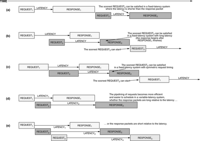
The patent application does not delve into the uses of this feature at all; the mechanism is presented simply, without justification or application. Our (educated) guess is that the mechanism is absolutely essential to the successful operation of the design—having a variable request latency is not an afterthought or flight of whimsy. Without variable request latencies, the support of variable burst lengths, and indeed the support of any burst length other than one equal to the length of a request packet or one smaller than the request latency, cannot function even tolerably well. This is illustrated in Figure 7.24. The figure shows what happens when a multiplexed, split transaction bus has back-to-back requests: if the request shapes are symmetric (e.g., the request and response packets are the same length, and the latency is slightly longer) or if the latency is long relative to the request and response packet lengths, then it is possible to pipeline requests and achieve good throughput, though neither scenario is optimal in bus efficiency. If the request packet and transaction latency are both short relative to the data transfer (a more optimal arrangement for a given request), later requests must be delayed until earlier requests finish, negating the value of having a split transaction bus in the first place (cf. Figure 7.24(a)). This is the most likely arrangement. Long data bursts are desirable, particularly if the target application is video processing or something similar. The potential problem is that these long data bursts necessarily generate asymmetric request-response shapes because the request packet should be as short as possible, dictated by the information in a request. If the DRAM supports variable request latencies, then the memory controller can pipeline requests, even those that have asymmetric shapes, and thus achieve good throughput despite the shape of the request.
Variable Block Size
Rambus’ 1990 patent application defines a mechanism that allows the memory controller to specify how much data should be transferred for a read or write request. The request packet that the memory controller sends to the DRAM device specifies the data length in the request packet’s BlockSize field. Possible data length values range from 0 bytes to 1024 bytes (1 KB). The amount of data that the DRAM sends out on the bus, therefore, is programmed at every transaction.
Like variable request latency, the variable block size feature is necessitated by the design of the bus. To dynamically change the transaction length from request to request would likely have seemed novel to an engineer in the early 1990s. The unique features of Rambus’ bus—its narrow width, multiplexed nature, and packet request protocol—place unique scheduling demands on the bus. Variable block size is used to cope with the unique scheduling demands; it enables the use of Rambus’ memory in many different engineering settings, and it helps to ensure that Rambus’ bus is fully utilized.
Running the Clock at the Data Rate
The design specifies a clock rate that can be half what one would normally expect in a simple, non-interleaved memory system. Figure 7.25 illustrates this, showing timing for two different clock arrangements. The top design is a more traditional arrangement; the bottom design uses a clock that is half the speed of the top design. Rambus’ 1990 application describes the clock design and its benefits as follows:

FIGURE 7.25 Running the bus clock at the data rate. Slowing down the clock so that it runs at the same speed as the data makes the clock easier to handle, but it reduces the number of clock edges available to do work. Clock edges exist to drive the output circuitry, but no clock edge exists during the eye of the data to sample the data.
Clock distribution problems can be further reduced by using a bus clock and device clock rate equal to the bus cycle data rate divided by two, that is, the bus clock period is twice the bus cycle period. Thus a 500 MHz bus preferably uses a 250 MHz clock rate. This reduction in frequency provides two benefits. First it makes all signals on the bus have the same worst case data rates—data on a 500 MHz bus can only change every 2 ns. Second, clocking at half the bus cycle data rate makes the labeling of the odd and even bus cycles trivial, for example, by defining even cycles to be those when the internal device clock is 0 and odd cycles when the internal device clock is 1.
As the inventors claim, the primary reason for doing so is to reduce the number of clock transitions per second to be equal to the maximum number of data transitions per second. This becomes important as clock speeds increase, which is presumably why IBM’s toggle mode uses the same technique. The second reason given is to simplify the decision of which edge to use to activate which receiver or driver (the labelling of “even/odd” cycles). Figure 10 in the specification illustrates the interleaved physical arrangement required to implement the clock-halving scheme: the two edges of the clock activate different input receivers at different times and cause different output data to be multiplexed to the output drivers at different times.
Note that halving the clock complicates receiving data at the DRAM end, because no clock edge exists during the eye of the data (this is noted in the figure), and therefore, the DRAM does not know when to sample the incoming data—that is, assuming no additional help. This additional help would most likely be in the form of a PLL or DLL circuit to accurately delay the clock edge so that it would be 90° out of phase with the data and thus could be used to sample the data. Such a circuit would add complexity to the DRAM and would consequently add cost in terms of manufacturing, testing, and power dissipation.
7.3.3 Comparison of Technologies in Rambus and JEDEC DRAM
The following paragraphs compare briefly, for each of four technologies, how the technology is used in a JEDEC-style DRAM system and how it is used in a Rambus-style memory system as described in the ′898 application.
Programmable CAS Latency
JEDEC’s programmable CAS latency is used to allow each system vendor to optimize the performance of its systems. It is programmed at system initialization, and, according to industry designers, it is never set again while the machine is running [Lee 2002, Baker 2002, Kellogg 2002, Macri 2002, Ryan 2002, Rhoden 2002, Sussman 2002]. By contrast, with Rambus’ variable request latency, the latency is programmed every time the microprocessor sends a new request to the DRAM, but the specification also leaves open the possibility that each access register could store two or more values held for each transaction type. Rambus’ system has the potential (and we would argue the need) to change the latency at a request granularity, i.e., each request could specify a different latency than the previous request, and the specification has room for many different latency values to be programmed. Whereas the feature is a convenience in the JEDEC organization, it is a necessity in a Rambus organization.
Programmable Burst Length
JEDEC’s programmable burst length is used to allow each system vendor to optimize the performance of its systems. It is programmed at system initialization, and, according to industry designers, it is never set again while the machine is running [Lee 2002, Baker 2002, Kellogg 2002, Rhoden 2002, Sussman 2002]. By contrast, with Rambus’ variable block size, the block size is programmed every time the microprocessor sends a new request to the DRAm. Whereas a JEDEC-style memory system can function efficiently if every column of data that is read out of or written into the DRAM is accompanied by a CAS signal, a Rambus-style memory system could not (as the command would occupy the same bus as the data, limiting data to less than half of the available bus cycles). Whereas the feature is a convenience in the JEDEC organization, it is a necessity in a Rambus organization.
Dual-Edged Clocking
Both JEDEC- and Rambus-style DRAMs use a clocking scheme that goes back at least to IBM’s high-speed toggle-mode DRAMs, in which on-chip interleaving allows one to toggle back and forth between two buffers (e.g., on the rising and falling edges of a strobe signal) to achieve a data rate that is twice that possible by a single buffer alone. Both JEDEC- and Rambus-style DRAMs transfer data on both edges of a timing signal. In JEDEC-style DRAMs, the timing signal is an internal clock generated from the system clock and the DQS data strobe—a source-synchronous strobe that accompanies the data sent and is quiescent when there is no data on the bus. The data is edge-aligned with the system clock. In Rambus-style DRAMs, the timing signal is a synthesized internal clock signal in synch with no other clock source in the system and generated from two different phases of the U-shaped global clock (described previously). The U-shaped clock is not source synchronous and remains free running whether there is data on the bus or not. As opposed to the DDR clocking scheme, in the Rambus scheme the data is not aligned with either phase of the system clock at all; it is neither edge-aligned nor center-aligned. Furthermore, a different phase relationship exists between each Rambus DRAM’s output data and the global clock’s early and late signals, whereas DDR DRAMs strive to maintain the same phase relationship between each DRAM’s output data and the system clock.
On-Chip PLL/DLL
JEDEC uses an on-chip DLL in their DDR SDRAMs to ensure that data being driven onto the data bus is aligned with the global clock signal. The DLL does this by delaying the DRAM’s response to a read request just long enough that the data is driven at the same time the DRAM sees the next clock edge. Rambus uses an on-chip variable delay circuit to ensure that every DRAM in the system as well as the memory controller has a synchronized clock (i.e., they all believe that it is precisely 12:00 at the same time). The delay circuit does this by finding the midpoint in time between an early version and a late version (i.e., two different phases) of the same clock signal and thereby creates a synthesized internal clock signal in synch with no other physical clock in the system. This is a process that is significantly more complicated than a simple DLL, and thus Rambus’ variable delay circuit is more complex than a simple DLL.
7.3.4 Alternative Technologies
Numerous alternative technologies could achieve the same result as the technologies described. Many of these alternatives are simply applications of long-understood techniques to solving particular problems. This section discusses a sample of those mechanisms; it is not intended to be exhaustive, but rather to be illustrative. This should give insight into issues that DRAM designers consider.
Programmable CAS Latency
The primary benefit of programmable CAS latency is flexibility. Its presence in a DRAM allows a fast part to emulate the behavior of a slow part, which would enable an OEM or end consumer to intermingle parts from different generations (with different speeds) in the same system or intermingle same-generation parts from different manufacturers (which might have slightly different performance capabilities due to slight variations in process technologies) in the same DIMm. To illustrate, if a DRAM manufacturer has a part with a minimum 20-ns CAS read-out, the part could conceivably work as a CAS-2, 100-MHz part (20 ns requires 2 cycles at 100 MHz); a CAS-3, 150-MHz part (20 ns requires 3 cycles at 150 MHz); or a CAS-4, 200-MHz part (20 ns requires 4 cycles at 200 MHz). Note that the part would never be able to make CAS-2 latencies at the higher bus speeds or CAS-3 at the highest bus speed (CAS-2 requires 13.33 ns at 150 MHz and 10 ns at 200 MHz; CAS-3 requires 15 ns at 200 MHz). Alternative technologies include the following:
• Use fixed CAS latency parts.
• Explicitly identify the CAS latency in the read or write command.
Use Fixed CAS Latency
Fixing the CAS latency would simply mean that each individual SDRAM would operate with a single, predetermined latency. Although using fixed latency would reduce flexibility, it would simplify testing considerably [Lee 2002], as only one mode of operation would need to be tested instead of two or more, and it would simplify design slightly. In a JEDEC-style bus organization, where the command, address, and data busses are all separate, the scheduling of requests is simplified if all requests have the same latency. Thus, memory controllers typically set the CAS latency at initialization and never change it again while the machine is powered on; i.e., current systems use a de facto fixed CAS latency while the machine is running [Lee 2002, Baker 2002, Kellogg 2002, Macri 2002, Ryan 2002, Rhoden 2002, Sussman 2002].
Explicitly Identify CAS Latency in the Command
One option would be to design the DRAM command set so that each column read command explicitly encodes the desired CAS latency. Instead of initializing the DRAM to use a latency of 2 or 3 cycles, and then presenting generic CAS commands, each of which would implicitly use a latency of 2 or 3 cycles, respectively, a memory controller could present commands to the SDRAM that would explicitly specify a desired latency. For example, the memory controller would use “CAS-2” read commands if it desired a latency of two and “CAS-3” read commands if it desired a latency of three.
Program CAS Latency Using Fuses
The CAS latency value could also be determined by the use of on-chip fuses. Modern DRAMs have numerous fuses on them that, when blown, enable redundant circuits, so at test time a DRAM manufacturer can, for example, disable memory arrays that contain fabrication errors and in their place enable redundant arrays that are error free. A typical DRAM has thousands of such fuses. One could add one or more similar fuses that set different CAS latencies. This would enable a DRAM manufacturer to sell what are essentially fixed-latency parts, but because they could be programmed at the last possible moment, the DRAM manufacturer would not need separate stocks for parts with different latencies; one part would satisfy for multiple latencies, as the DRAM manufacturer could set the fuses appropriately right before shipping the parts. The manufacturer could also sell the parts with fuses intact to OEMs and embedded-systems manufacturers, who would likely have the technical savvy necessary to set the fuses properly, and who might want the ability to program the latency according to their own needs. This level of flexibility would be almost on par with the current level of flexibility, since in most systems the CAS latency is set once at system initialization and never set again.
Scale CAS Latency with Clock Frequency
One option is for the DRAM to know the bus speed and deliver the fastest CAS latency available for that bus speed. The programming of the DRAM could be either explicit, in which case the memory controller tells the DRAM the bus speed using a command at system initialization, or implicit, in which case the DRAM senses the timing of the clock on the bus and “learns” the bus speed on its own. To return to the earlier example, if a DRAM part had an internal CAS read-out latency of 20 ns, it could deliver CAS-2 in a 100-MHz/10-ns bus environment, CAS-3 in a 133-MHz/7.5-ns bus environment, and CAS-4 in a 200-MHz/5-ns bus environment. This would satisfy most DRAM consumers, because OEMs and end-users usually want the fastest latency possible. However, without an additional mechanism in either the DRAM or the memory controller, the scheme would not allow parts with different internal CAS read-out latencies to be mixed within the same system. Disallowing mixed-latency systems would not cause undue confusion in the marketplace, because asynchronous parts in the 1980s and 1990s were sold as “70ns DRAMs” or “60ns DRAMs,” etc.; the speed rating was explicit, so both OEMs and end-users were already accustomed to matching speed ratings in their systems. However, if support for mixed-latency systems was desired, one could always design the memory controller so that it determines at initialization the latency of each DIMM in its system11 and accounts for any latency differences between DIMMs in its scheduling decisions.
Programmable Burst Length
In JEDEC-style DRAM systems, the ability to set the burst length to different values is a convenience for system designers that can also system performance. Numerous subtle interactions between the chosen parameters of a DRAM system (such as request latency, burst length, bus organization, bus speed, and bus width) can cause the resulting performance of that system to vary significantly, even for small changes in those parameters [Cuppu & Jacob 2001]. The ability to fine-tune the burst length of the DRAMs enables a designer to find better combinations of parameters for his system, given the expected workload. In most systems, the burst length is set once at system initialization and never set again [Lee 2002, Baker 2002, Kellogg 2002, Rhoden 2002, Sussman 2002]. Alternative technologies include the following:
• Use a short, fixed burst length.
• Explicitly identify the burst length in the read or write command.
• Program the burst length by blowing fuses on the DRAm.
• Use a long, fixed burst length coupled with the burst-terminate command.
• Use a BEDO-style protocol where each CAS pulse toggles out a single column of data.
The first three are analogous to the alternative solutions for programmable CAS latency, described above.
Use Burst-Terminate Command
One can use a fixed burst length, where the length is some number large enough to satisfy developers of systems that prefer large chunks of data, and use the burst-terminate command, also called burst stop, to halt data read-out of the DRAM or to signal the end of data written to the DRAm. The advantage of the scheme is that the burst stop command is already part of the specification, and bursts must also be interruptible by additional commands such as reads and writes. Therefore, an efficient pipeline of multiple column reads is already possible by simply sending multiple read commands spaced as closely as the desired burst length dictates (e.g., every four cycles to achieve a burst length of four, even if the nominal burst length is longer). Each successive request would implicitly terminate the request immediately preceding it, and only the last burst in the pipeline would need to be terminated explicitly. The disadvantage of the scheme is that it would increase pressure slightly on the command bus: during a burst-terminate command the memory controller would not be able to control any other bank on the same command bus. If the increase was determined to be significant, it could be alleviated by redesigning the memory controller to support multiple control busses (which is already supported by memory controllers).
Toggle Data-Out Using CAS
JEDEC could have adopted the BEDO style of bursting data, with each successive column read-out driven by toggling the CAS pin or holding it at a low voltage until the desired number of columns has been read out (e.g., holding it low for four cycles to read out four columns of data). This would require some modification to the specification, enabling the DRAM to distinguish between a CAS accompanied by a new column address and a CAS signifying a serial read-out based on the most recent column address received. There are numerous possibilities for solving this, including the following:
• Redefine the command set to have two different CAS commands: one for a new address, and one signifying a sequential read-out based on the most recent column address received.
• Add a pin to the command bus (which is usually thought of as comprising signals such as RAS, CAS, WE, and CKE) that is dedicated for the sequential read-out version of CAs. This would be similar to IBM’s implementation of the high-speed toggle mode, where the data strobe signal uses a different pin than the CAS signal [Kalter 1990a, b].
The advantage of the second scheme, as compared to the first, is that it allows the memory controller to control other DRAM banks simultaneously while the first bank is involved in data transfer.
Dual-Edged Clocking
The advantage of using dual-edged clocking in a JEDEC-style DRAM bus organization is that it increases DRAM bandwidth without having to drive the clock any faster and without a commensurate increase in the clock signal’s energy consumption. Alternative technologies include the following:
• Use two or more interleaved memory banks on-chip and assign a different clock signal to each bank (e.g., use two or more out-of-phase clocks).
• Keep each DRAM single data rate, and interleave banks on the module (DIMM).
• Increase the number of pins per DRAm.
Interleave On-Chip Banks
As mentioned earlier, interleaving multiple memory banks has been a popular method used to achieve high-bandwidth memory busses using low-bandwidth devices. The technique goes back at least to the mid-1960s, where it was used in the IBM System/360 Model 91 [Anderson et al. 1967] and Seymour Cray’s Control Data 6600 [Thornton 1970]. In an interleaved memory system, the data bus uses a frequency that is faster than any one DRAM bank can support; the control circuitry toggles back and forth between multiple banks to achieve this data rate. An alternative to using dual-edged clocking (e.g., to double or triple or even quadruple the memory bandwidth of SDRAM without using both edges of the clock to send/receive data) is to specify two, three, or four independent banks per DRAM (respectively) and assign each bank its own clock signal. The memory controller would send one request to the DRAM, and that request would be handed off to each bank in synch with the clock assigned to that bank. Thus, each bank would receive its request slightly advanced or delayed with respect to the other banks. There are two ways to create the different clock signals:
• The different clock signals driving each of the different banks could be generated by the memory controller (or any entity outside the DRAM). Thus, if there were two interleaved banks, the memory controller would send two clock signals; if there were four interleaved banks, the memory controller would send four clock signals; and so on.
• The DRAM could receive one clock signal and delay and distribute it internally to the various banks on its own. Thus, if there were two interleaved banks, the DRAM would split the incoming clock signal two ways, delaying the second a half-phase; if there were four interleaved banks, the DRAM would split the incoming clock signal four ways, delaying the second clock one-quarter of a phase, delaying the third clock one-half of a phase, and delaying the last clock three-quarters of a phase; and so on.
The first implementation would require extra DRAM pins (one CK pin for each bank); the latter would require on-DRAM clock generation and synchronization logic.
Interleave Banks on the Module
Instead of increasing the bandwidth of individual DRAMs, an argument could be made that the only place it matters is at the DIMM level. Therefore, one could take SDRAM parts and create a DDR DIMM specification where on-module circuitry takes a single incoming clock and interleaves two or more banks of DRAM (transparently, as far as the memory controller is concerned). Kentron [2002] shows that this is certainly within our limits, even at very high data rates; they currently take DDR parts and interleave them transparently at the module level to achieve quadruple data rate DIMMs.
Increase DRAM Data Width
To achieve higher bandwidth per DRAM, the trend in recent years has been not only to increase DRAM speed, but also to increase the number of data-out pins; x32 parts are now common. Every increase from x4 to x8 to x16 and so on doubles the DRAM’s data rate. Doubling the data rate by doubling the data width of existing parts requires very little engineering know-how. It only requires the addition of more pins and doubling the width of the data bus to each individual DRAm. Note that the number of data pins has increased from x1 parts in the late 1980s to x32 parts today [Przybylski 1996], while over the same time period the data rate has increased from 16 MHz to the 400-MHz clocks found in DDR SDRAM today. JEDEC, therefore, could have simply put their weight more firmly behind this trend and increased bandwidth by increasing pin-out. The advantage of this approach is that it combines very well with the previous alternative—interleaving multiple banks at the module level—because doubling the data width of a DRAM decreases the number of DRAM parts needed to achieve the DIMM data width, effectively doubling the number of independent banks one can put on the DIMm. If the DRAM pin-out increases, then fewer DRAMs would be needed per DIMM to create the 64-bit data bus standard in PC-compatible systems. This would leave extra room on the DIMM for more DRAMs that could make up extra banks to implement an interleaved system.
Increase Module Data Width
As mentioned earlier, one could argue that the DIMM bandwidth is more important than the bandwidth of an individual DRAm. Therefore, one could simply increase the data width of the memory bus (the number of wires between the DIMMs and the memory controller) to increase bandwidth, without having to increase the clock speed of the individual DRAMs at all. The disadvantage is the increased cost of the de-skewing circuitry.
Double the Clock Frequency
An alternative to using a dual-edged clock is to use a single-edged clock and simply speed up the clock. There are several advantages of a single-edged clocking scheme over a dual-edged clocking scheme (cf. Figure 7.20). One advantage illustrated in Figure 7.20 is the existence of more clock edges to be used to drive data onto the bus and sample data off the bus. Another advantage is that the clock does not need to be as symmetric as it is in a dual-edged clocking scheme. A single-edged clock’s duty cycle does not need to be 50%, as it needs to be for a dual-edged clock, and the rise and fall times (i.e., slew rates) do not need to match, as they need to for a dual-edged clock. Consequently, one can achieve the same speed clock in a single-edged clocking scheme with much less effort than in a dual-edged clocking scheme. The disadvantage of this alternative is that it requires more engineering effort than simply widening the memory bus or increasing the number of data pins on a DRAm.
Use Simultaneous Bidirectional I/O
Running the data at the same rate as the clock doubles a DRAM’s bandwidth over previous, single-edged clock designs without an increase in the number of data pins. An alternative is to use simultaneous bidirectional I/O, in which it is possible to conduct a read from the DRAM and a write to the DRAM at exactly the same time; that is, both data values (the read data and the write data) are on the bus simultaneously, which is an effective doubling of the available bandwidth. Using the simultaneous bidirectional I/O does not require additional data pins. Such a scheme would require structural changes at the DRAM side to accommodate reading and writing simultaneously, and those changes would most likely resemble the ESDRAM design by Enhanced Memory Systems [ESDRAM 1998], which was proposed for DDR2 [Davis et al. 2000b]. ESDRAM places a buffer after the sense amps that holds an entire DRAM row for reading and allows concurrent writes to the DRAM array; once the read data is in the buffer, the sense amplifiers are no longer needed.
On-Chip PLL/DLL
DDR SDRAMs use an on-chip DLL circuit to ensure that the DRAM transmits its data and DQS signal to the memory controller as closely as possible to the next appropriate edge of the system clock. Its use is specified because the clock rates in DDR are high enough to warrant relatively strong methods for reducing the effects of dynamic changes in timing skew. Alternative technologies include the following:
• Achieve high bandwidth using more DRAM pins or module pins, not clock frequency.
• Use a Vernier method to measure and account for dynamic changes in skew.
• Put the DLL on the memory controller.
Go Wider, Not Faster
As the previous section indicates, there are numerous ways to achieve higher bandwidth at the DRAM, DIMM, or memory-system level, and many of the methods that achieve higher bandwidth are easier to implement than increasing clock speed. The use of a DLL is dictated only by the desired increase in clock speed. Therefore, one can forgo the use of an on-chip DLL by increasing DRAM or DIMM data width.
Vernier Mechanism
There are two main components to the uncertainty of signal propagation time. The first is a static component that is due to differences in process technologies, process variations, electrical loading of an unknown number of memory modules, etc. The second is a dynamic component that is typically due to temperature or voltage fluctuations. Some fluctuations change too fast to be handled effectively, but most of the fluctuations in voltage and temperature change over a relatively long time period. Most voltage fluctuations are associated with the 60-Hz AC power cycle, which is a relatively long time-span, and most temperature fluctuations occur on the order of milliseconds or longer [Lee 2002, Macri 2002]. In many DDR systems, the static component is corrected by using a Vernier mechanism in the memory controller at system initialization. It is essentially a trial-and-error method in which the upper and lower limits of timing failure are found and the midpoint is used for signal transmission (analogous to setting the tracking on one’s VCR by going forward and backward to the points of noise and then leaving the tracking set somewhere in between) [Lee 2002]. The dynamic component is then corrected by the on-chip DLL.
An alternative to the on-chip DLL is to perform recalibration of the Vernier correction often enough to account for the slower changes in voltage and temperature, as opposed to performing the timing correction only once at system initialization. Assuming that the most significant voltage fluctuations are associated with the 60-Hz AC power supply and that most of the temperature fluctuations occur on the order of milliseconds or longer [Lee 2002, Macri 2002], recalibration would be needed roughly once or twice every millisecond.
Move the DLL onto the Memory Controller
Because the DLL is only used on the DRAM to synchronize outgoing data and DQS signals with the global clock for the benefit of the memory controller [Lee 2002, Rhoden 2002, Karabotsos 2002, Baker 2002, Macri 2002], it is possible to move that functionality onto the memory controller itself. The memory controller could maintain two clocks: the first, for example, could be synchronized with the global clock, and the second could be delayed 90°. The incoming DQS and data signals could be given a variable delay, with the amount of delay controlled by a DLL/PLL on the memory controller so that the DQS signal would be in-phase with the delayed clock. This arrangement could align the incoming data so that the eye would be centered on the global clock signal, which could be used to sample the data. The weakness of this scheme is that, as clock speeds increase to very high rates, the timing differences between different DIMMs would become significant. Therefore, each DIMM in the system would require a different phase shift between the memory controller’s two clocks, which would imply that the memory controller would need to maintain a separate timing structure for each DIMm.12
Move the DLL onto the DIMM
One alternative is to place the DLL on the DDR module instead of the DDR device itself. Sun has used this alternative for many years [Becker 2002, O’Donnell 2002, Prein 2002, Walker 2002]. Moreover, it is similar in nature to the off-chip driver mechanism used by IBM in their high-speed toggle-mode DRAM [Kalter 1990a, b]. As mentioned previously, the only function of the DLL on the DDR SDRAM is to synchronize the outgoing DQS and data signals with the global clock. This can be accomplished just as easily on the module, especially if the module is buffered or registered (which simply means that the module has local storage to hold the commands and addresses that are destined for the module’s DRAMs). Note that it is presently common practice for engineers to disable DDR’s on-chip DLL to achieve higher performance—the on-chip DLL is a convenience, not a necessity [Rhoden 2002, Kellogg 2002, Macri 2002]. A module-level DLL is perfectly workable; even if the data exiting the DRAM is completely out of synch with the global clock, the module can use its DLL to delay the clock/s, commands, and addresses so that the output of the DRAMs is in synch with the global clock. However, this might come at the expense of an extra CAS latency cycle.
7.4 Fully Buffered DIMM: A Compromise of Sorts
An interesting development in the DRAM industry is the recent introduction of the fully buffered DIMM (FB-DIMM). This is a system-level DRAM organization developed by Intel that, at first glance, looks a bit like a compromise between a traditional JEDEC wide-bus design and a Rambus-like narrow-bus design. Chapter 14 explores the FB-DIMM in more detail. Here, we will simply introduce it and present a motivation for its development.
An important trend facing system designers ultimately argues for FB-DIMM or something like it. As DRAM technology has advanced, the channel speed has improved at the expense of channel capacity. SDR SDRAMs could populate a channel with eight DIMMs. DDR SDRAMs operate at a higher data rate and limit the number of DIMMs to four per channel. DDR2 SDRAMs operate at an even higher data rate and limit the number of DIMMs to two per channel. DDR3 is expected to limit the number of DIMMs per channel to one. This is a significant limitation; for a server designer, it is critical, as servers typically depend on memory capacity for their performance.
The trend is clear: to improve data rates, one must reduce the number of drops on the bus. The designers of graphics subsystems have known this for a long time—for every DRAM generation, graphics cards use the same DRAM technology as is found in commodity DIMMs, but the graphics cards operate their DRAMs at significantly higher data rates because they use point-to-point connections. Note that this is possible in a marketing sense because graphics cards are de facto embedded systems. Users do not expect to upgrade their graphics cards by adding more memory to them; they instead replace the entire card.
So there is an obvious dilemma: future designers would like both increased channel capacity and increased data rates. How can one provide both?
The relationship between a modular organization and the graphics-card organization is shown in Figure 7.26, which depicts a multi-drop DRAM bus next to a DRAM bus organization typical of graphics cards. The graphics-card organization uses the same DRAM technology as in the multi-drop organization, but it also uses point-to-point soldered connections between the DRAM and memory controller and can therefore reach higher rates of speed. How can one exploit this to increase data rates without sacrificing channel capacity? One solution is to redefine one’s terms—to call the graphic-card arrangement a “DIMM” in one’s future system. This is shown on the right-hand side of the figure and is precisely what is happening in FB-DIMM: the memory controller has been moved onto the DIMM, and all connections in the system are point-to-point. The channel connecting the master memory controller to the DIMM-level memory controllers (called Advanced Memory Buffers, or AMBs) is very narrow and very fast, based on the PCI-X standard. Moreover, each DIMM-to-DIMM connection is a point-to-point connection, making an entire channel a de facto multi-hop store and forward network. The FB-DIMM architecture limits the channel length to eight DIMMs, and the width of the inter-module bus is narrow enough to require roughly one-third the number of pins as a traditional organization. The result is that an FB-DIMM organization can handle roughly 24 times the storage capacity as a traditional DDR3-based system (assuming DDR3 systems will indeed be limited to one DIMM per channel), without sacrificing any bandwidth and even leaving room for increased intra-module bandwidth (note that the FB-DIMM module should be capable of reaching the same performance as a graphics-card organization).

FIGURE 7.26 Motivation for the design of FB-DIMm. The first two organizations compare a modular wide-bus and a high-performance embedded system such as a graphics card. Above each design is its side profile, indicating potential impedance mismatches (sources of relections). The organization on the far right shows how FB-DIMM takes the graphics-card organization as its de facto DIMm. In the FB-DIMM organization, there are no multi-drop busses; DIMM-to-DIMM connections are point-to-point.
7.5 Issues in DRAM Systems, Briefly
The previous section already touched on an important issue facing the system designers of tomorrow: bandwidth increases are not free and require some form of trade-off. The traditional approach has been to reduce the number of drops on the shared bus, but this approach cleary fails to scale. The Overview section described other issues, namely that protocol-level details interact with system-level organization parameters in non-intuitive ways that can reduce performance by factors of two or more. There are many other issues facing future DRAM systems, and these will be treated in more detail in the upcoming chapters. The following is a brief introduction to several of the issues.
7.5.1 Architecture and Scaling
The bandwidth improvements in each DRAM generation have come at a cost in channel capacity, but they have also come at a cost in the granularity of access. Through a trick of trading off space for time, DRAM designers have increased the data rate at the DRAM’s I/O pins without having also to increase the speed of the DRAM’s core. DDR improves speed relative to single data rate (SDR) by moving to a 2n prefetch architecture—one in which twice the number of bits are fetched from the DRAM core. The bandwidth increase on one side of the interface is matched by a bandwidth increase on the other side; the I/O side is twice as fast, and the core side is twice as wide (on the I/O side of the DRAM, bits are transmitted twice as fast as before; on the core side, twice as many bits are fetched in a single cycle). DDR2 improves speed again by moving to 4n prefetch; DDR3 is expected to implement 8n prefetch. In each instance, the minimum number of bits that the DRAM can read or write increases by a factor of two. The implication is that processors need to double the amount of data that they read and write in each operation, but the question remains as to how far a cache block will scale before SRAM designers say enough: 128 B per block? 256 B? 1 KB?
7.5.2 Topology and Timing
As previously discussed, there is a direct connection between signal integrity and system organization; changes to the system organization can significantly improve or degrade signal integrity. The same is true of bus topologies. For example, designers of unidirectional busses do not need to concern themselves with turnaround time, a limitation on throughput when the masters of bi-directional buses change. A related issue is that of the timing convention used. When the topology changes, the timing convention may need to be changed to follow suit. Unidirectional busses would tend to work better with source-synchronous clocking, for example, but source-synchronous clocking is not as simple as a global clocking scheme.
7.5.3 Pin and Protocol Efficiency
Pin cost is becoming a major concern; the cost of a transistor or a capacitor on-die is reducing at a tremendous rate, and packaging costs are not decreasing as rapidly. The obvious conclusion is that in the future, DRAM design will be far more concerned about pin count than transistor count. The only way to reduce significantly the number of pins needed in a part, without also significantly reducing the part’s data bandwidth (e.g., by simply reducing the number of data pins on the package), is to rethink the protocol and allow a trade-off between pins used for data and control (address, command, etc).
7.5.4 Power and Heat Dissipation
DRAMs have traditionally not accounted for much of a design’s power or heat dissipation. For instance, DRAMs typically do not come with heat sinks, nor do DIMMs. However, with modern inter-chip signaling rates exceeding 1 Gbps per pin (as in present-day FB-DIMMs), both power dissipation and heat dissipation become serious issues. Previous-era DIMMs exhibited power dissipation on the order of 1 W. Current FB-DIMMs dissipate nearly ten times that. Couple this with the ability to put 25 times the number of FB-DIMMs into a system (three times as many channels, eight times as many DIMMs per channel), and you now have a significant heating problem. Modern blade servers are a popular design choice and work because only a handful of components in the system dissipate significant heat, and DRAM was never one of these. Now, the DRAM subsystem threatens to complicate blade-server design, among other things.
7.5.5 Future Directions
Currently, much of the focus in future DRAM design has been placed on increasing bandwidth via increased pin rates. This only scales well for a limited design window. In particular, it places too much emphasis on optimizing the device and not enough on optimizing the system. This is precisely the type of narrow-scope thinking that has led to the systemic problems described in the Overview chapter: designers thinking only at the device level can create system-level problems, just as designers thinking only at the system level can create device-level problems.
The solution is non-trivial, because it requires facing economic arguments. DRAM is a device that tries to suit many different needs. A design solution must work just as well in a DIMM organization as being soldered directly to a motherboard, talking one-on-one with the microprocessor. In other words, in many cases the device is the system. How to marry these two perspectives will be an ongoing concern.
1A “strobe” is a signal that indicates to the recipient that another signal, e.g., data or command, is present and valid.
2This step is necessary for SDRAMs; it is not performed for older, asynchronous DRAMs (it is subsumed by the earlier chip-select accompanying the RAS).
3One bit in a “x1” DRAM, two bits in a “x2” DRAM, four bits in a “x4” DRAM, etc.
4The term “normal” implies the data cycling at half the data-strobe rate.
5In practice, this is not the case, as the memory controller and DRAM subsystem are driven by the system clock, which typically has a period that is an integral multiple of the microprocessor’s clock.
6By some estimates, BEDO actually had higher performance than SDRAM [Williams 2001].
7Making an interface synchronous is a well-known technique to simplify the interface and to ease scaling to higher switching speeds [Stone 1982].
8There is also significant discussion (and illustration) in the patent application describing Rambus’ unorthodox/revolutionary proposed packaging technology, in which a DRAM’s pins are all on one edge of the chip and in which the chips are inserted directly into a backplane-type arrangement individually, as opposed to being integrated onto a memory module.
9In a PC system, the data bus is 64 bits; the address bus can be 16 bits; and there can be 10 or more control lines, as the number of chip-select lines scales with the number of memory modules in the system.
10A “bus cycle” is the period during which a bus transaction takes place, which may correspond to one clock cycle, more than one clock cycle, or less than one clock cycle.
11One would probably not want to create a DIMM out of DRAM parts with different fixed CAS latencies.
12Most DLLs/PLLs require many cycles to lock onto a signal and create the correct phase shift. Forcing the memory controller to wait many cycles before switching from reading from one DIMM to reading from another DIMM would be an unsatisfactory situation.