
DRAM System Signaling and Timing
In any electronic system, multiple devices are connected together, and signals are sent from one point in the system to another point in the system for the devices to communicate with each other. The signals adhere to predefined signaling and timing protocols to ensure correctness in the transmission of commands and data. In the grand scale of things, the topics of signaling and timing require volumes of dedicated texts for proper coverage. This chapter cannot hope to, nor is it designed to, provide a comprehensive coverage on these important topics. Rather, the purpose of this chapter is to provide basic terminologies and understanding of the fundamentals of signaling and timing—subjects of utmost importance that drive design decisions in modern DRAM memory systems. This chapter provides the basic understanding of signaling and timing in modern electronic systems and acts as a primer for further understanding of the topology, electrical signaling, and protocols of modern DRAM memory systems in subsequent chapters. The text in this chapter is written for those interested in the DRAM memory system but do not have a background as an electrical engineer, and it is designed to provide a basic survey of the topic sufficient only to understand the system-level issues that impact the design and implementation of DRAM memory systems, without having to pick up another text to reference the basic concepts.
9.1 Signaling System
In the decades since the emergence of electronic computers, the demand for ever-increasing memory capacity has constantly risen. This insatiable demand for memory capacity means that the number of DRAM devices attached to the memory system for a given class of computers has remained relatively constant despite the increase in per-device capacity made possible with advancements in semiconductor technology. The need to connect multiple DRAM devices together to form a larger memory system for a wide variety of computing platforms has remained unchanged for many years. In the cases where multiple, discrete DRAM devices are connected together to form larger memory systems, complex signaling systems are needed to transmit information to and from the DRAM devices in the memory system.
Figure 9.1 illustrates the timing diagram for two consecutive column read commands to different DDR SDRAM devices. The timing diagram shows idealized timing waveforms, where data is moved from the DRAM devices in response to commands sent by the DRAM memory controller. However, as Figure 9.1 illustrates, signals in real-world systems are far from ideal, and signal integrity issues such as ringing, attenuation, and non-monotonic signals can and do negatively impact the setup and hold time requirements of signal timing constraints. Specifically, Figure 9.1 illustrates that a given signal may be considered high-quality if it transitions rapidly and settles rapidly from one signal level to another. Figure 9.1 further illustrates that a poorly designed signaling system can result in a poor quality signal that overshoots, undershoots, and does not settle rapidly into its new signal value, possibly resulting in the violation of the setup time or the hold time requirements in a high-speed system.
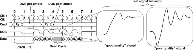
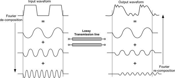
Figure 9.2 illustrates the fundamental problem of frequency-dependent signal transmission in a lossy, real-world transmission line. That is, an input waveform, even an idealized, perfect square wave signal, can be decomposed into a Fourier series—a sum of sinusoidal and cosinusoidal oscillations of various amplitudes and frequencies. The real-world, lossy transmission line can then be modelled as a non-linear low-pass filter where the low-frequency components of the Fourier decomposition of the input waveform pass through the transmission line without substantial impact to their respective amplitudes or phases. In contrast, the non-linear, low-pass transmission line will significantly attenuate and phase shift the high-frequency components of the input waveform. Then, recomposition of the various frequency components of the input waveform at the output of the lossy transmission line will result in an output waveform that is significantly different from that of the input waveform.
Collectively, constraints of the signaling system will limit the signaling rate and the delivery of symbols between discrete semiconductor devices such as DRAM devices and the memory controller. Consequently, the construction and assumptions inherent in the signaling system can and do directly impact the access protocol of a given memory system, which in turn determines the bandwidth, latency, and efficiency characteristics of the memory system. As a result, a basic comprehension of issues relating to signaling and timing is needed as a foundation to understand the architectural and engineering design trade-offs of modern, multi-device memory systems.
Figure 9.3 shows a basic signaling system where a symbol, encoded as a signal, is sent by a transmitter along a transmission line and delivered to a receiver. The receiver must then resolve the value of the signal transmitted within valid timing windows determined by the synchronization mechanism. The signal should then be removed from the transmission line by a resistive element, labelled as the terminator in Figure 9.3, so that it does not interfere with the transmission and reception of subsequent signals. The termination scheme should be carefully designed to improve signal integrity depending on the specific interconnect scheme. Typically, serial termination is used at the receiver and parallel termination is used at the transmitter in modern high-speed memory systems. As a general summary, serial termination reduces signal ringing at the cost of reduced signal swing at the receiver, and parallel termination improves signal quality, but consumes additional active power to remove the signal from the transmission line.
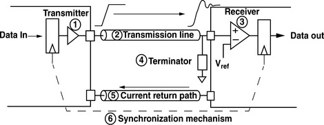
Figure 9.3 illustrates a basic signaling system where signals are delivered unidirectionally from a transmitter to a single receiver. In contemporary DRAM memory systems, signals are often delivered to multiple DRAM devices connected on the same transmission line. Specifically, in SDRAM and SDRAM-like DRAM memory systems, multiple DRAM devices are often connected to a given address and command bus, and multiple DRAM devices are often connected to the same data bus where the same transmission line is used to move data from the DRAM memory controller to the DRAM devices, as well as from the DRAM devices back to the DRAM memory controller.
The examination of the signaling system in this chapter begins with an examination of basic transmission line theory with the treatment of wires as ideal transmission lines, and it proceeds to an examination of the termination mechanism utilized in the DRAM memory system. However, due to their relative complexity and the limited coverage envisioned in this chapter, specific circuits utilized by DRAM devices for signal transmission and reception are not examined herein.
9.2 Transmission Lines on PCBs
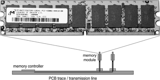
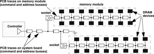
Modern DRAM memory systems are typically formed from multiple devices mounted on printed circuit boards (PCBs). The interconnects on PCBs are mostly wires and vias that allow an electrical signal to deliver a symbol from one point in the system to another point in the system. The symbol may be binary (1 or 0) as in all modern DRAM memory systems or may, in fact, be multi-valued, where each symbol can represent two or more bits of information. The limitation on the speed and reliability of the data transport mechanism in moving a symbol from one point in the system to another point in the system depends on the quality and characteristics of the traces used in the system board. Figure 9.4 illustrates a commodity DRAM memory module, where multiple DRAM devices are connected to a PCB, and multiple memory modules are connected to the memory controller through more PCB traces on the system board. In contemporary DRAM memory systems, multiple memory modules are then typically connected to a system board where electrical signals that represent different symbols are delivered to the devices in the system through traces on the different PCB segments.
In this section, the electrical properties of signal traces are examined by first characterizing the electrical characteristics of idealized transmission lines. Once the characteristics of idealized transmission lines have been established, the discussion then proceeds to examine the non-idealities of signal transmission on a system board such as attenuation, reflection, skin effect, crosstalk, inter-symbol interference (ISI), and simultaneous switching outputs (SSO). The coverage of these basic topics will then enable the reader to proceed to understand system-level design issues in modern, high-speed DRAM memory systems.
9.2.1 Brief Tutorial on the Telegrapher’s Equations
To begin the examination of the electrical characteristics of signal interconnects, an understanding of transmission line characteristics is a basic requirement. This section provides the derivation of the telegrapher’s equations that will be used as the basis of understanding the signal interconnect in this chapter.
Figure 9.5 illustrates that an infinitesimally small piece of transmission line can be modelled as a resistive element R that is in series with an inductive element L, and these elements are parallel to a capacitive element C and a conductive element G. To understand the electrical characteristics of the basic transmission line, Kirchhoff’s voltage law can be applied to the transmission line segment in Figure 9.5 to obtain Equation 9.1,
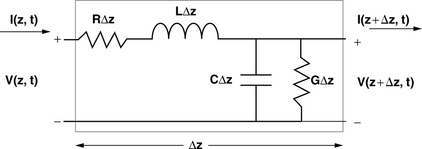
FIGURE 9.5 Mathematical model of a basic transmission line. Top wire (+) is signal; bottom wire (−) is signal return.

and Kirchhoff’s current law can be applied to the same transmission line segment in Figure 9.5 to obtain Equation 9.2.
Then, dividing Equations 9.1 and 9.2 through by ΔZ, and taking the limit as ΔZ approaches zero, Equation 9.3 can be derived from Equation 9.1, and Equation 9.4 can be derived from Equation 9.2.
Equations 9.3 and 9.4 are time-domain equations that describe the electrical characteristics of the transmission line. Equations 9.3 and 9.4 are also known as the Telegrapher’s Equations.1
Furthermore, Equations 9.3 and 9.4 can be solved simultaneously to obtain steady-state sinusoidal wave equations. Equations 9.5 and 9.6 are derived from Equations 9.3 and 9.4, respectively,
where γ is represented by Equation 9.7.
Furthermore, solving for voltage and current equations, Equations 9.8 and 9.9 are derived
where V0+ and V0− are the respective voltages, and I0+ and I0− are the respective currents that exist at locations Z+ and Z−, locations infinitesimally close to reference location Z. That is, Equations 9.8 and 9.9 are the standing wave equations the describe transmission line characteristics.
Finally, rearranging Equations 9.8 and 9.9, Equations 9.10 and 9.11 can be derived
where Z0 is the characteristic impedance, and α and β are the attenuation constant and the phase constant of the transmission line, respectively. Although the characteristic impedance of the transmission line has the unit of ohms, it is conceptually different from simple resistance. Rather, the characteristic impedance is the resistance seen by propagating waveforms at a specific point of the transmission line.
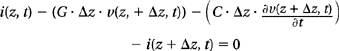
9.2.2 RC and LC Transmission Line Models
Equations 9.1–9.11 illustrate a mathematical derivation of basic transmission line characteristics. However, system designer engineers are often interested in transmission line behavior within relatively narrow frequency bands rather than the full frequency spectrum. Consequently, simpler high-frequency LC (Inductor-Capacitor) or low-frequency RC (Resistor-Capacitor) models are often used in place of the generalized model. Figure 9.6 shows the same model for an infinitesimally small piece of transmission line as in Figure 9.5, but a closer examination of the characteristic impedance equation reveals that the equation can be simplified if the magnitude of the resistive component R is much smaller than or much greater than the magnitude of the frequency-dependent inductive component jωL. That is, in the case where the magnitude of R greatly exceeds jωL, the characteristic impedance of the transmission line can be simplified as Z0 = SQRT(R/jωC),2 hereafter referred to as the RC model. Conversely, in the case where the magnitude of the frequency-dependent inductive component jωL greatly exceeds the magnitude of the resistive component R, the characteristic impedance of the transmission line can be simplified as Z0 = SQRT(L/C), hereafter referred to as the LC model. Given that the general transmission line model can be simplified into the LC model or the RC model, the key to choosing the correct model is to compute the characteristic frequency f0 for the transmission line where the resistance R equals jωL. The characteristic frequency f0 can be computed with the equation f0 = R / 2πL. The simple rule of thumb that can be used is that for operating frequencies much above f0, system designer engineers can assume a simplified LC transmission line model, and for operating frequencies much below f0, system designer engineers can assume a simplified RC transmission line model. Due to the fact that signal paths on silicon are highly resistive, the characteristic frequency f0 is much lower for silicon interconnects than system interconnects. As a result, the RC model is typically used for silicon interconnects on silicon, and the LC model is typically used for package-level and system-level interconnects.
9.2.3 LC Transmission Line Model for PCB Traces
Figure 9.7 shows the cross section of a six-layer PCB. The six-layer PCB consists of signaling layers on the top and bottom layers with two more signaling layers sandwiched between two metal planes devoted to power and ground. Typically, inexpensive PC systems use only four-layer PCBs due to cost considerations, while more expensive server systems and memory modules typically use PCBs with six, eight, or more layers (on some systems, upwards of twenty-plus layers) for better signal shielding, signal routing, and power supplies.

Figure 9.7 also shows a close-up section of a trace on the uppermost signaling layer and the respective electrical characteristics of that signal trace. Given the resistive component of the signal trace as 0.003 Ω/mm and the inductance component of the signal trace as 0.25 nH/mm, the characteristic frequency of the signal trace can be computed as 1.9 MHz. That is, the signal traces on the illustrated PCB can be modelled effectively—to the first order—by relying only on the LC characteristics of the transmission line, since the edge transition frequencies of signals in contemporary DRAM memory systems are considerably higher than 1.9 MHz.3
9.2.4 Signal Velocity on the LC Transmission Line
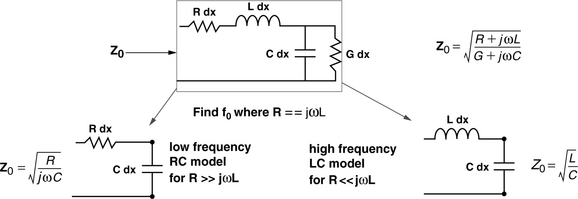
The electrical characteristics of the transmission line derived in Equations 9.1-9.11 and discussed in the previous section assert that typical PCB traces in modern DRAM memory systems can be typically modelled as LC transmission lines. In this and the following sections, properties of typical PCB traces are further examined to qualify signal traces found on contemporary PCBs from idealized LC transmission lines.
Figure 9.8 illustrates two important characteristics of the ideal LC transmission line: the wave velocity and the superposition property of signals that travel on the transmission line. In an ideal LC transmission line, the resistive element is assumed to be negligible, and signals can theoretically propagate down an ideal LC transmission line without attenuation. Figure 9.8 also shows that the signal propagation speed on an ideal lossless LC transmission line is a function of the impedance characteristics of the LC transmission line, and signal velocity can be computed with the equation 1/SQRT(LC). Substituting in the capacitance and inductance values from Figure 9.7, the wave velocity of an electrical signal as it propagates on the specific transmission line is computed to be 200,000,000 M/s. That is, on the transmission line with the specific impedance characteristics, signal wave-fronts propagate at two-thirds the speed of light in vacuum, and signal wave-fronts travel a distance of 20 cm/ns.
Finally, in the lossless LC transmission line, signals can propagate down the transmission line without interference from signals propagating in the opposite direction. In this manner, the transmission line can support bidirectional signaling, and the voltage at a given point on the transmission line can be computed by the instantaneous superposition of the signals propagating on the transmission line.
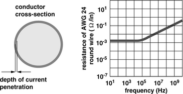
9.2.5 Skin Effect of Conductors
The skin depth effect is a critical component of signal attenuation. That is, the resistance of a conductor is typically a function of the cross-sectional area of the conductor, and the resistance of a signal trace is typically held as a constant in the computation of transmission line characteristics. However, one interesting characteristic of conductors is that electrical current does not flow uniformly throughout the cross section of the conductor at high frequencies. Instead, current flow is limited to a certain depth of the conductor cross section when the signal is switching rapidly at high frequencies. The frequency-dependent current penetration depth is illustrated as the skin depth in Figure 9.9. The net effect of the limited current flow in conductors at high frequencies is that resistance of a conductor increases as a function of frequency. The skin effect of conductors further illustrates that a lossless ideal LC transmission line cannot completely model a real-world PCB trace.
9.2.6 Dielectric Loss
The LC transmission line is often used as a first-order model that approximates the characteristics of traces on a system board. However, real-world signal traces are certainly not ideal lossless LC transmission lines, and signals do attenuate as a function of trace length and frequency. Figure 9.10 illustrates signal attenuation through a PCB trace as a function of trace length and data rate. The figure shows that signal attenuation increases at higher data rates and longer trace lengths. In the context of a DRAM memory system, a trace that runs for 10 inches and operates at 500 Mbps will lose less than 5% of the peak-to-peak signal strength. Moreover, Figure 9.10 shows that signal attenuation remains below 10% for the 10” trace that operates at data rates upward to 2.5 Gbps. In this sense, the issue of signal attenuation is a manageable issue for DRAM memory systems that operate at relatively modest data rates and relatively short trace lengths. However, the issue of signal attenuation is only one of several issues that system design engineers must account for in the design of high-speed DRAM memory systems and one of several issues that ensures the lossless LC transmission line model remains only as an approximate first-order model for PCB traces.

FIGURE 9.10 Attenuation factor of a signal on a PCB trace. Graph taken from North East Systems Associates Inc. Copyright 2002, North East Systems Associates Inc. with permission.
One common way to model dielectric loss is to place a distributed shunt conductance across the line whose conductivity is proportional to frequency. Most transmission lines exhibit quite a large metallic loss from the skin effect at frequencies well below those where dielectric loss becomes important. In most modern memory systems, signal reflection is typically a far more serious problem for the relatively short trace length, multi-drop signaling system. For these reasons, dielectric loss is often ignored, but its onset is very fast when it does happen. For DDR2 SDRAM and other lower speed memory systems (<1 Gbps), dielectric loss is not a dominant effect and can be generally ignored in the signaling analysis. However, in higher data rate memory systems such as the Fully Buffered DIMM and DDR3 memory systems, dielectric loss should be considered for complete signaling analysis.
The physics of the dielectric loss can be described with basic electron theory. The dielectric material between the conductors is an insulator, and electrons that orbit the atoms in the dielectric material are locked in place in the insulating material. When there is a difference in potential between two conductors, the excessive negative charge on one conductor repels electrons on the dielectric toward the positive conductor and disturbs the orbits of the electrons in the dielectric material. A change in the path of electrons requires more energy, resulting in the loss of energy in the form of attenuating voltage signals.
9.2.7 Electromagnetic Interference and Crosstalk
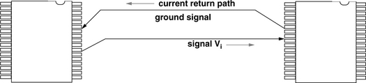
In an electrical signaling system, the movement of a voltage signal delivered through a transmission line involves the displacement of electrons in the direction of, or opposite to the direction of, the voltage signal delivery. The conservation of charge, in turn, means that as current flows in one direction, there must exist a current that flows in the opposite direction. Figure 9.11 shows that current flow on a transmission line must be balanced with current flow through a current return path back to the originating device. Collectively, the signal current and the return current form a closed-circuit loop. Typically, the return current flow occurs through the ground plane or an adjacent signal trace. In effect, a given signal and its current return path form a basic current loop where the magnitude of the current flow in the loop and the area of the loop determine the magnitude of the Electromagnetic Interference (EMI). In general, EMI generated by the delivery of a signal in a system creates inductive coupling between signal traces in a given system. Additionally, signal traces in a closely packed system board will also be susceptible to capacitive coupling with adjacent signal traces.
In this section, electronic noises injected into a given trace by signaling activity from adjacent traces are collectively referred to as crosstalk. Crosstalk may be induced as the result of a given signal trace’s capacitive or inductive coupling to adjacent traces. For example, in the case where a signal and its presumed current return path (signal ground) are not routed closely to each other, and a different trace is instead routed closer to the signal trace than the current return path of the signal trace, this adjacent (victim) trace will be susceptible to EMI that emanates from the poorly designed current loop, resulting in crosstalk between the signal traces. The issue of crosstalk further deviates the modelling of real-world system board traces from the idealities of the lossless LC transmission line, where closely routed signal traces can become attackers on their neighboring signal traces and significantly impact the timing and signal integrity of these neighboring traces. The magnitude of the crosstalk injected by capacitively or inductively coupled signal traces depends on the peak-to-peak voltage swings of the attacking signals, the slew rate of the signals, the distance of the traces, and the travel direction of the signals.
To minimize crosstalk in high-speed signaling systems, signal traces are often routed closely with a dedicated current return path and are then routed with the dedicated current return path shielding active signal traces from each other. In this manner, the minimization of the current loop reduces EMI, and the spacing of active traces and the respective current return paths also reduces capacitive coupling. Unfortunately, the use of dedicated current return paths increases the number of traces required in the signaling system. As a result, dedicated shielding traces are typically found only in high-speed digital systems. For example, high-speed memory systems such as Rambus Corp’s XDR memory system rely on differential traces over closely routed signaling pairs to ensure high signaling quality in the system, while lower cost, commodity-market-focused memory systems such as DDR2 SDRAM reserve differential signaling to clock signal and high-speed data strobe signals.
9.2.8 Near-End and Far-End Crosstalk
In general, two types of crosstalk effects exist in signal systems: near-end crosstalk and far-end crosstalk. These two types of crosstalk effects are, respectively, illustrated in Figures 9.12 and 9.13. Although Figures 9.12 and 9.13 illustrate crosstalk for capacitively coupled signal traces, near-end and far-end crosstalk effects are similar for inductively coupled signal traces. Figures 9.12 and 9.13 show that as a voltage signal travels from the source to the destination, it generates eletronic noises in an adjacent trace. At each point on the transmission line, the attacking signal generates a victim signal on the victim trace. The victim signal will then travel in two directions: in the same direction as the attacker signal and in the opposite direction of the attacker signal. Figure 9.12 shows that the victim signal traveling in the opposite direction of the attacker signal will result in a relatively long duration, low-amplitude noise at the near (source) end of the victim trace.

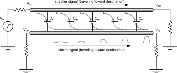
In contrast, Figure 9.13 shows that the electronic noise traveling in the same direction as the attacker signal will result in a victim signal that is relatively short in duration, but high in amplitude at the far (destination) end of the victim signal trace. In essence, the near-end and far-end crosstalk effects can be analogized to the Doppler effect. That is, as the attacker signal wave front moves from the source to the destination on a given transmission line, it creates sympathetic signals in closely coupled victim traces that are routed in close proximity. The sympathetic signals that travel backward toward the source of the attacking signal will appear as longer wavelengths and lower amplitude noise, and sympathetic signals that travel in the same direction as the attacking signal will add up to appear as a short wavelength, high-amplitude noise.
Finally, an interesting general observation is that since the magnitude of the crosstalk depends on the magnitude of the attacking signals, an increase in the signal strength of one signal in the system would, in turn, increase the magnitude of the crosstalk experienced by other traces in the system, and the increase in signal strength of all signals in the system, in turn, exacerbates the crosstalk problem on the system level. Consequently, the issue of crosstalk must be solved by careful system design rather than a simple increase in the strength of signals in the system.
9.2.9 Transmission Line Discontinuities
In an ideal LC transmission line with uniform characteristic impedance throughout the length of the transmission line, a signal can, in theory, propagate down the transmission line without reflection or attenuation at any point in the transmission line. However, in the case where the transmission line consists of multiple segments with different characteristic impedances for each segment, signals propagating on the transmission line will be altered at the interface of each discontinuous segment.
Figure 9.14 illustrates that at the interface of any two mismatched transmission line segments, part of the incident signal will be transmitted and part of the incident signal will be reflected toward the source. Figure 9.14 also shows that the characteristics of the mismatched interface can be described in terms of the reflection coefficient ρ, and ρ can be computed from the formula ρ = (ZL − ZS)/(ZL + ZS). With the formula for the reflection coefficient, the reflected signal at the interface of two transmission line segments can be computed by multiplying the voltage of the incident signal and the reflection coefficient. The voltage of the transmitted signal can be computed in a similar fashion since the sum of the voltage of the transmitted signal and the voltage of the reflected signal must equal the voltage of the incident signal.
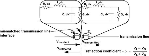
In any classroom discussion about the reflection coefficient of transmission line discontinuities, there are three special cases that are typically examined in detail: the well-matched transmission line segments, the open-circuit transmission line, and the short-circuit transmission line. In the case where the characteristic impedances of two transmission line segments are matched, the reflection coefficient of that interface ρ is 0 and all of the signals are transmitted from one segment to another segment. In the case that the load segment is an open circuit, the reflection coefficient is 1, the incident signal will be entirely reflected toward the source, and no part of the incident signal will be transmitted across the open circuit. Finally, in the case where the load segment is a short circuit, the reflection coefficient is – 1, and the incident signal will be reflected toward the source with equal magnitude but opposite sign.
Figure 9.15 illustrates a circuit where the output impedance of the voltage source is different from the impedance of the transmission line. The transmission line also drives a load whose impedance is comparable to that of an open circuit. In the circuit illustrated to the figure, there are three different segments, each with a different characteristic impedance. In this transmission line, there are two different impedance discontinuities. Figure 9.15 shows that the reflection coefficients of the two different interfaces are represented by ρ (source) and ρ (load), respectively. Finally, the figure also shows that the transmission line segment that connects the source to the load has finite length, and the signal flight time is 250 ps on the transmission line between the mismatched interfaces.
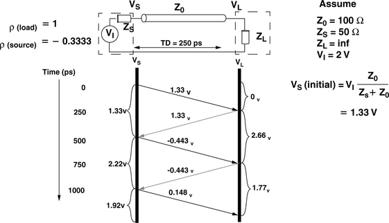
Figure 9.15 shows the voltage ladder diagram where the signal transmission begins with the voltage source driving a 0-V signal prior to time zero and switching instantaneously to 2 V at time zero. The figure also shows that the initial voltage VS can be computed from the basic voltage divider formula, and the initial voltage is computed and illustrated as 1.33 V. The ladder diagram further shows that due to the signal flight time, the voltage at the interface of the load, VL, remains at 0 V until 250 ps after the incident signal appears at Vs. The 1.33-V signal is then reflected with full magnitude by the load with the reflection coefficient of 1 back toward the voltage source. Then, after another 250 ps of signal flight time, the reflected signal reaches the interface between the transmission line and the voltage source. The reflected signal with the magnitude of 1.33 V is then itself reflected by the transmission line discontinuity at the voltage source, and the re-reflected signal of –0.443 V once again propagates toward the load.
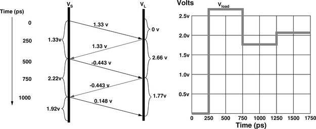
Figure 9.16 illustrates that the instantaneous voltage on a given point of the transmission line can be computed by the sum of all of the incident and reflected signals. The figure also illustrates that the superposition of the incident and reflected signals shows that the output signal at VL appears as a severe ringing problem that eventually converges around the value driven by the voltage source, 2 V. However, as the example in Figure 9.16 illustrates, the convergence only occurs after several round-trip signal flight times on the transmission line.
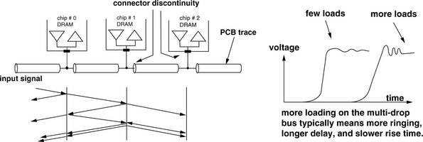
9.2.10 Multi-Drop Bus
In commodity DRAM memory systems such as SDRAM, DDR SDRAM, and similar DDRx SDRAM, multi-drop busses are used to carry command, address, and data signals from the memory controller to multiple DRAM devices. Figure 9.17 shows that from the perspective of the PCB traces that carry signals on the system board, each DRAM device on the multi-drop bus appears as an impedance discontinuity. The figure shows an abstract ladder diagram where a signal propagating on the PCB trace will be partly reflected and transmitted across each impedance discontinuity. Typical effects of signal propagation across multiple impedance discontinuities are more ringing, a longer delay, and a slower rise time.
The loading characteristics of a multi-drop bus, as illustrated in Figure 9.17, means that the effects of impedance discontinuities must be carefully controlled to enable a signaling system to operate at high data rates. As part of the effort to enable higher data rates in successive generations of DRAM memory systems, specifications that define tolerances of signal trace lengths, impedance characteristics, and the number of loads on the multidrop bus have become ever more stringent. For example, in SDRAM memory systems that operate with the data rate of 100 Mbps, as many as eight SDRAM devices can be connected to the data bus, but in DDR3 SDRAM memory systems that operate with the data rate of 800 Mbps and above, the initial specification requires that no more than two devices can be connected to the same data bus in a connection scheme referred to as point-to-two-point (P22P), where the controller is specified to be limited to the connection of two DRAM devices located adjacent to each other.
9.2.11 Socket Interfaces
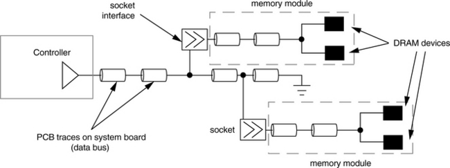
One feature that is demanded by end-users in commodity DRAM memory systems is the feature that allows the end-user to configure the capacity of the DRAM memory system by adding or removing memory modules as needed. However, the use of memory modules means that socket interfaces are needed to connect PCB traces on the system board to PCB traces on the memory modules that then connect to the DRAM devices. Socket interfaces are highly problematic for a transmission line in the sense that a socket interface represents a capacitive discontinuity for the transmission line, even in the case where the system only has a single memory module and the characteristic impedances of the traces on the system board and the memory module are well matched to each other.
To ensure that DRAM memory systems can operate at high data rates, memory system design engineers must carefully model each component of the memory system as well as the overall behavior of the system in response to a signal injected into the system. Figure 9.18 illustrates an abstract model of the data bus of a DDR SDRAM memory system, and it shows that a signal transmitted by the controller will first propagate on PCB traces in the system board. As the propagated signal encounters a socket interface, part of the signal will be reflected back toward the controller and part of the signal will continue to propagate down the PCB trace, while most of the signal will be transmitted through the socket interface onto the memory module where the signal continues propagation toward the DRAM devices.
9.2.12 Skew
Figure 9.8 shows that wave velocity on a transmission line can be computed with the formula 1/SQRT(LC). For the transmission line with the specific impedance characteristics given in Figure 9.8, a signal would travel through the distance of 20 cm/ns. As a result, any signal path lengths that are not well matched to each other in terms of distances would introduce some amounts of timing skew between signals that travel on those paths.
Figure 9.19 illustrates the concept of signal skew in a poorly designed signaling system. In Figure 9.19, two signal traces carry signals on a parallel bus from the controller to modules labelled as module A and module B. Figure 9.19 shows that due to the poor design, path 1 which carries bus signal #1 is shorter than path 2 which carries bus signal #2. In this system, the different path lengths introduce static skew between bus signal #1 and bus signal #2.
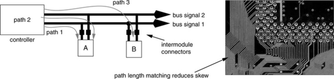
FIGURE 9.19 Mismatched path lengths introduces signal-to-signal skew, and PCB with path-length-matched signal traces.
In this chapter, skew is defined as the timing differential between two signals in a system. Skew can exist between data signals of a wide parallel data bus or between data signals and the clock signal. Moreover, signal skew can be introduced into a signaling system by differences in path lengths or the electrical loading characteristics of the respective signal paths. As a result, skew minimization is an absolute requirement in the implementation of high-speed, wide, and parallel data busses. Fortunately, the skew component of the timing budget is typically static, and with careful design, the impact of the data-to-data and data-to-clock skew can be minimized. For example, the PCB image in Figure 9.19 shows the trace routing on the system board of a commodity personal computer, and it illustrates that system design engineers often purposefully add extra twists and turns to signal paths to minimize signal skew between signal traces of a parallel bus.
9.2.13 Jitter
In the broad context of analog signaling, jitter can be defined as unwanted variations in amplitude or timing between successive pulses on a given signal line. In this chapter, the discussion on jitter is limited to the context of DRAM memory systems with digital voltage levels, and only the short-term phase variations that exist between successive cycles of a given signal are considered. For example, electronic components are sensitive to short-term variations in supply voltage and temperature, and effects such as crosstalk depend on transitional states of adjacent signals. Collectively, the impact of short-term variations in supply voltage, temperature, and crosstalk can vary dramatically between successive cycles of a given signal. As a result, the propagation time of a signal on a given signal path can exhibit subtle fluctuations on a cycle-by-cycle basis. These subtle variations in timing are defined as jitter on a given signal line.
To ensure correctness of operation, signaling systems account for timing variations introduced into the system by both skew and jitter. However, due to the unpredictable nature of the effects that cause jitter, it is often difficult to fully characterize jitter on a given signal line. As a result, jitter is also often more difficult than skew to deal with in terms of timing margins that must be devoted to account for the timing uncertainty.
9.2.14 Inter-Symbol Interference (ISI)
In this chapter, crosstalk, signal reflections, and other effects that impact signal integrity and timing are examined separately. However, the result of these effects can be summarized in the sense that they all degrade the performance of the signaling system. Additionally, multiple, consecutive signals on the same transmission line can have collective, residual effects that can interfere with the transmission of subsequent signals on the same transmission line. The intra-trace inference is commonly referred to as inter-symbol interference (ISI).
Inter-symbol interference is intrinsically a band-pass filter issue. The interconnect is a non-linear low-pass filter. The energy of the driver signal resides mostly within the third harmonic frequency. But the interconnect low-pass filter is non-linear, which causes the dispersion of the signal. In other words, a given signal that is not promptly removed from the transmission medium by the signal termination mechanism may disperse slowly and affect later signals that make use of the same transmission medium. For example, a single pulse has a long tail beyond its “ideal” pulse range. If there are consecutive “1”s, the accumulated tails may add up to overwrite the following “0.” The net effect of ISI is that the interference degrades performance and limits the signaling rate of the system.
9.3 Termination
Previous sections illustrate that signal propagation on a transmission line with points of impedance discontinuity will result in multiple signal reflections, with one set of reflections at each point of impedance discontinuity. Specifically, the example in Figure 9.15 shows that in a system where the input impedance of the load4 differs significantly from the characteristic impedance of the transmission line, the impedance discontinuity at the interface between the transmission line and the load results in multiple, significant signal reflections that delay the settle time of the transmitted signal. To limit the impact of signal reflection at the end of a transmission line, high-speed system design engineers typically place termination elements whose resistive value matches the characteristic impedance of the transmission line. The function of the termination element is to remove the signal from the transmission line and eliminate the signal reflection caused by the impedance discontinuity at the load interface. Figure 9.20 shows the placement of the termination element ZT at the end of the transmission line. Ideally, in a well-designed system, the resistive value of the termination element, ZT, matches exactly the characteristic impedance of the transmission line, Z0. The signal is then removed from the transmission line by the termination element, and no signal is reflected toward the source of the signal.
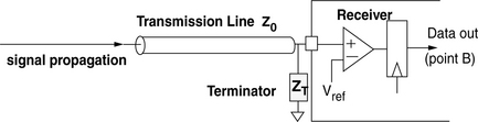
FIGURE 9.20 A well-matched termination element removes the signal at the end of the transmission line.
9.3.1 Series Stub (Serial) Termination
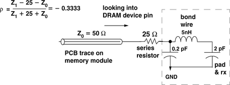
The overriding consideration in the design and standardization process of modern DRAM memory systems designed for the commodity market is the cost of the DRAM devices. To minimize the manufacturing cost of the DRAM devices, relatively low-cost packaging types such as SOJ and TSOP are used in SDRAM memory systems, and the TSOP is used in DDR SDRAM memory systems.5
Unfortunately, the input pin of the low-cost SOJ and TSOP packages contains relatively large inductance and capacitance characteristics and typically represents a poorly matched load for any transmission line. The poorly matched impedance between the system board trace and device packages is not a problem for DRAM memory systems with relatively low operating frequencies (below 200 MHz). However, the mismatched impedance issue gains more urgency with each attempt to increase the data rate of the DRAM memory system.
Figure 9.21 shows the series stub termination scheme used in DDR SDRAM memory systems. Unlike the ideal termination element, the series stub terminator is not designed to remove the signal from the transmission line once the signal has been delivered to the receiver. Rather, the series resistor is designed to increase the damping ratio and to provide an artificial impedance discontinuity that isolates the complex impedances within the DRAM package, resulting in the reduction of signal reflections back onto the PCB trace from within the DRAM device package.
9.3.2 On-Die (Parallel) Termination
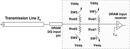
The use of series termination resistors in SDRAM and DDR SDRAM memory systems to isolate the complex impedances within the DRAM device package means that the burden is placed on system design engineers to add termination resistors to the DRAM memory system. In DDR2 and DDR3 SDRAM devices, the use of the higher cost Fine Ball Grid Array (FBGA) package enables DRAM device manufacturers to remove part of the inductance that exists in the input pins of SOJ and TSOP packages. As a result, DDR2 and DDR3 SDRAM devices could then adopt an on-die termination scheme that more closely represents the ideal termination scheme illustrated in Figure 9.20.
Figure 9.22 shows that in DDR2 devices, depending on the programmed state of the control register and the value of the on-die termination (ODT) signal line, switches SW1 and SW2 can be controlled independently to provide different termination values as needed. The programmability of the on-die termination of DDR2 devices, in turn, enables the respective DRAM devices to adjust to different system configurations without having to assume worst-case system configurations.
9.4 Signaling
In DRAM memory systems, the signaling protocol defines the electrical voltage or current levels and the timing specifications used to transmit and receive commands and data in a given system. Figure 9.23 shows the eye diagram for a basic binary signaling system commonly used in DRAM memory systems, where the voltage values V0 and V1 represent the two states in the binary signaling system. In the figure, tcycle represents the cycle time of one signal transfer in the signaling system. The cycle time can be broken down into different components: the signal transition time ttran, the skew and jitter timing budget tskew, and the valid bit time teye.

To achieve high operating data rates, the cycle time, tcycle, must be as short as possible. The goal in the design and implementation of a high-speed signaling system is then to minimize the time spent by signals on state transition, account for possible skew and jitter, and respect signal setup and hold time requirements. The voltage and timing requirements of the signaling protocol must be respected in all cases regardless of the existence of transient voltage noises such as those caused by crosstalk or transient timing noises such as those caused by temperature-dependent signal jitter. In the design and verification process of high-speed signaling systems, eye diagrams such as the one illustrated in Figure 9.23 are often used to describe the signal quality of a signaling system. A high-quality signaling system with properly matched and terminated transmission lines will minimize skew and jitter, resulting in eye diagrams with well-defined eye openings and minimum timing and voltage uncertainties.
9.4.1 Eye Diagrams
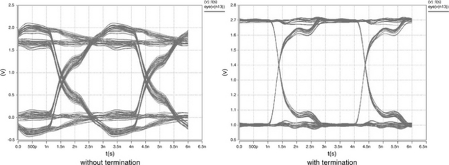
Figure 9.24 is an example that shows the practical use of eye diagrams. The eye diagram of a signal in a system designed without termination is shown on the left, and the eye diagram of a signal in a system designed with termination is shown on the right. Figure 9.24 illustrates that in a high-quality signaling system, the eye openings are large, with clearly defined voltage and timing margins. As long as the eye opening of the signal remains intact, buffers can effectively eliminate voltage noises and boost binary voltage levels to their respective maximum and minimum values. Unfortunately, timing noises cannot be recovered by a simple buffer, and once jitter is introduced into the signaling system, the timing uncertainty will require a larger timing budget to account for the jitter. Consequently, a longer cycle time and lower data rate may be needed to ensure the correctness of signal transmission in the system—for a poorly designed signaling system.
9.4.2 Low-Voltage TTL (Transistor-Transistor Logic)
Figure 9.25 illustrates the input and output voltage response for a low-voltage TTL (LVTTL) device. The LVTTL signaling protocol is used in SDRAM memory systems and other DRAM memory of its generation, such as Extended Data-Out DRAM (EDO DRAM), Virtual Channel DRAM (VCDRAM), and Enhanced SDRAM (ESDRAM) memory systems. The LVTTL signaling specification is simply a reduced voltage specification of the venerable TTL signaling specification that operates with a 3.3-V voltage supply rather than the standard 5- V voltage supply.
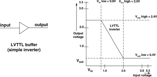
Similar to the TTL devices, LVTTL devices do not supply voltage references to the receivers of the signals. Rather, the receivers are expected to provide internal references so that input voltages lower than 0.8 V are resolved as one state of the binary signal and input voltages higher than 2.0 V are resolved as the alternate state of the binary signal. LVTTL devices are expected to drive voltage-high output signals above 2.4 V and low output signals below 0.4 V. For a LVTTL signal to switch state, the signal must traverse a large voltage swing. The large voltage swing and the large voltage range of undefined state between 0.8 and 2.0 V effectively limits the use of TTL and LVTTL signaling protocols to relatively low-frequency systems. For example, SDRAM memory systems are typically limited to operating frequencies below 167 MHz. Subsequent generations of DRAM memory systems have since migrated to more advanced signaling protocols such as Series Stub Terminated Logic (SSTL).
9.4.3 Voltage References
In modern DRAM memory systems, voltage-level-based signaling mechanisms are used to transport command, control, address, and data from the controller to and from the DRAM devices. However, for the delivered signals to be properly resolved by the receiver, the voltage level of the delivered signals must be compared to a reference voltage. While the use of implicit voltage references in TTL and LVTTL devices is sufficient for the relatively low operating frequency ranges and generous voltage range of the TTL and LVTTL signaling protocols, implicit voltage references are inadequate in modern DRAM memory systems that operate at dramatically higher data rates and with far smaller voltage ranges. As a result, voltage references are used in modern DRAM memory systems just as they are typically used in high-speed ASIC signaling systems.
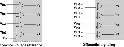
Figure 9.26 illustrates two common schemes for reference voltage comparison. The diagram on the left illustrates the scheme where multiple input signal pins share a common voltage reference that is delivered by the transmitter along with the data signals. The diagram on the right shows differential signaling where each signal is delivered with its complement. The common voltage scheme is used in DRAM memory systems where low cost predominates over the requirement of high data rate, and differential signaling is used to achieve a higher data rate at the cost of higher pin count in high-speed DRAM memory systems. Aside from the advantage of being able to make use of the full voltage swing to resolve signals to one state or another, complementary pinpairs are always routed closely together, and the minimal distance allows differential pin pairs to exhibit superior common-mode noise rejection characteristics.
9.4.4 Series Stub Termination Logic
Figure 9.27 illustrates the voltage levels used in 2.5-V Series Stub Termination Logic signaling (SSTL_2). SSTL_2 is used in DDR SDRAM memory systems, and DDR2 SDRAM memory systems use SSTL_18 as the signaling protocol. SSTL_18 is simply a reduced voltage version of SSTL_2, and SSTL_18 is specified to operate with a supply voltage of 1.8 V.
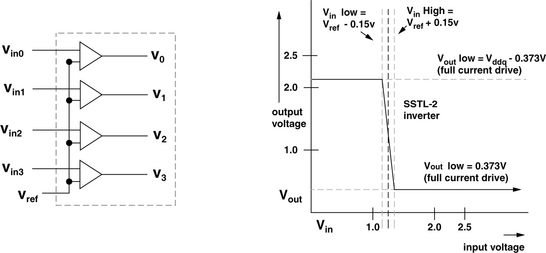
Figure 9.27 shows that, unlike LVTTL, SSTL_2 signaling makes use of a common voltage reference to accurately resolve the value of the input signal. The figure further shows that where Vref is set to 1.25 V, signals in the range of 0 to 1.1 V at the input of the SSTL_2 buffer are resolved as voltage low and signals in the range of 1.4 to 2.5 V are resolved as voltage high. In this manner, SSTL_2 exhibits better noise margins for the low-voltage range and nearly comparable noise margins for the high-voltage range when compared to LVTTL despite the fact that the supply voltage used in SSTL_2 is far lower than the supply voltage used in LVTTL.6
9.4.5 RSL and DRSL
In recent years, Rambus Corp. introduced two different signaling systems that are used in two different high-speed DRAM memory systems. The Rambus signaling level (RSL) signaling protocol was used in the Direct RDRAM memory system, and the differential Rambus signaling level (DRSL) signaling protocol was used in the XDR memory system. RSL and DRSL are interesting due to the fact that they are different from LVTTL and SSTL-x signaling protocols.
Figure 9.28 illustrates that both RSL and DRSL utilize low-voltage swings compared to SSTL and LVTTL. In SSTL and LVTTL signaling systems, signals swing the full voltage range from 0 V to Vddq, enabling a common voltage supply level for the DRAM core as well as the signaling interface at the cost of longer signal switch times. In the RSL signaling system, signals swing from 1.0 to 1.8 V; in the DRSL signaling system, signals swing from 1.0 to 1.2 V. While the low voltage swing enables fast signal switch time, the different voltage levels mean that the signaling interface must be carefully isolated from the DRAM core, thus requiring more circuitry on the DRAM device.
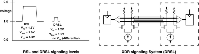
Finally, Figure 9.28 shows that similar to SSTL, RSL uses a voltage reference to resolve signal states, but DRSL does not use shared voltage references. Rather, DRSL is a bidirectional point-to-point differential signaling protocol that uses current mirrors to deliver signals between the memory controller and XDR DRAM devices.
9.5 Timing Synchronization
Modern digital systems, in general, and modern DRAM memory systems, specifically, are often designed as synchronous state machines. However, the address, command, control, data, and clock signals in a modern high-speed DRAM memory system must all propagate on the same type of signal traces in PCBs. As a result, the clock signal is subject to the same issues of signal integrity and propagation delay that impact other signals in the system. Figure 9.29 abstractly illustrates the problem in high-speed digital systems, where the propagation delay of the clock signal may be greater than a non-negligible fraction of a clock period. In such a case, the notion of synchronization must be reexamined to account for the phase differences in the distribution of the clock signal.
In general, there are three types of clocking systems used in synchronous DRAM memory systems: a global clocking system, a source-synchronous clock forwarding system, and a phase or delay compensated clocking system. The global clocking system assumes that the propagation delay of the clock signal between different devices in the system is relatively minor compared to the length of the clock period. In such a case, the timing variance due to the propagation delay of the clock signal is simply factored into the timing margin of the signaling protocol. As a result, the use of global clocking systems is limited to relatively lower frequency DRAM memory systems such as SDRAM memory systems. In higher data rate DRAM memory systems such as Direct RDRAM and DDR SDRAM memory systems, the global clocking scheme is replaced with source-synchronous clock signals to ensure proper synchronization for data transport between the memory controller and the DRAM devices. Finally, as signaling data rates continue to climb, ever more sophisticated circuits are deployed to ensure proper synchronization for data transport between the memory controller and the DRAM devices. Specifically, Phase-Locked Loop (PLL) or Delay-Locked Loop (DLL) circuits are used in DRAM memory controllers to actively compensate for signal skew. In the following sections, the clocking schemes used in modern DRAM memory systems to enable system synchronization are examined.
9.5.1 Clock Forwarding
Figure 9.30 illustrates the trivial case where a reference clock signal is sent along with the data signal from the transmitter to the receiver. The clock forwarding technique is used in DRAM memory systems such as DDR SDRAM and Direct DRAM, where subsets of signals that must be transported in parallel from the transmitter to the receiver are routed with clock or strobe signals that provide the synchronization reference. For example, the 16-bit-wide data bus in Direct RDRAM memory systems is divided into two sets of signals with separate reference clock signals for each set, and DDR SDRAM memory systems provide separate DQ strobe signals to ensure that each 8-bit subset of the wide data bus has an independent clocking reference.
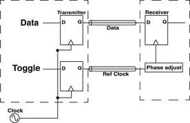
The basic assumption here is that by routing the synchronization reference signal along with a small groups of signals, system design engineers can more easily minimize variances in the electrical and mechanical characteristics between a given signal and its synchronization reference signal, and the signal-to-clock skew is minimized by design.
Figure 9.30 also shows that the concept of clock forwarding can be combined with more advanced circuitry that further minimizes signal-to-clock skew.
9.5.2 Phase-Locked Loop (PLL)
Two types of circuits are used in modern digital systems to actively manage the distribution and synchronization of the clock signal: a PLL and a DLL. PLLs and DLLs are used in modern high-speed DRAM devices to adjust and compensate for the skew and buffering delays of the clock signal. Figure 9.31 illustrates a basic block diagram of a PLL that uses an input clock signal and a voltage-controlled oscillator (VCO) in a closed-loop configuration to generate an output clock signal. With the use of the VCO, a PLL is capable of adjusting the phase of the output clock signal relative to the input clock signal, and it is also capable of frequency multiplication. For example, in an XDR memory system where the data bus interface operates at a data rate of 3.2 Gbps, a relatively low-frequency clock signal that operates at 400 MHz is used to synchronize data transfer between the memory controller and the DRAM devices. In the XDR DRAM memory system, PLL circuits are used to multiply the 400-MHz clock frequency and generate a 1.6-GHz output clock signal from the slower input clock frequency. The devices in the XDR memory system then make use of the phase-compensated 1.6-GHz clock signal as the clock reference signal for data movement. In this manner, two silicon devices can operate synchronously at relatively high frequencies without the transport of a high-frequency clock signal on the system board.
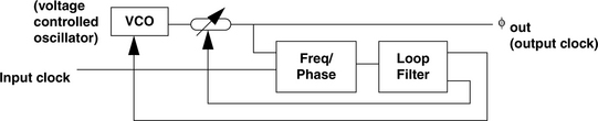
PLLs can be implemented as a discrete semiconductor device, but they are typically integrated into modern high-speed digital semiconductor devices such as microprocessors and FPGAs. Depending on the circuit implementation, PLLs can be designed to lock in a range of input clock frequencies and provide the phase compensation and frequency multiplication needed in modern high-speed digital systems.
9.5.3 Delay-Locked Loop (DLL)
Figure 9.32 illustrates the basic block diagram of a DLL. The difference between the DLL and the PLL is that a DLL simply inserts a voltage-controlled phase delay between the input and output clock signals. In a PLL, a voltage-controlled oscillator synthesizes a new clock signal whose frequency may be a multiple of the frequency of the input clock signal, and the phase delay of the newly synthesized clock signal is also adjustable for active skew compensation. In this manner, while DLLs only delay the incoming clock signals, the PLLs actually synthesize a new clock signal as the output.

The lack of a VCO means that DLLs are simpler to implement and more immune to jitter induced by voltage supply or substrate noise. However, since DLLs merely add a controllable phase delay to the input clock signal and produce an output clock signal, jitter that is present in the input clock signal is passed directly to the output clock signal. In contrast, the jitter of the input clock signal can be better filtered out by a PLL.
The relatively lower cost of implementation compared to PLLs makes DLLs attractive for use in commodity DRAM devices designed to minimize manufacturing costs and in any application where clock synthesis is not required. Specifically, DLLs are found in DRAM devices such as DDRx SDRAM and GDDRx (Graphics DDRx) devices.7
9.6 Selected DRAM Signaling and Timing Issues
Signaling in DRAM memory systems is alike in many ways to signaling in logic-based8 digital systems and different in other ways. In particular, the challenges of designing high data rate signaling systems such as proper impedance matching, skew, jitter, and crosstalk minimization, as well as a system synchronization mechanism, are the same for all digital systems. However, commodity DRAM memory systems such as SDRAM, DDR SDRAM, and DDR2 SDRAM have some unique characteristics that are unlike high-speed signaling systems in non-DRAM-based digital systems. For example, in commodity DRAM memory systems, the burdens of timing control and synchronization are largely placed in the sophisticated memory controllers, and commodity DRAM devices are designed to be as simple and as inexpensive to manufacture as possible. The asymmetric master-slave relationship between the memory controller and the multiple DRAM devices also constrains system signaling and timing characteristics of commodity DRAM memory systems in ways not commonly seen in more symmetric logic-based digital systems.
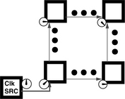
Figure 9.18 illustrates the data bus structure of a commodity DRAM memory system. Figure 9.33 illustrates the command and address bus structure of the same DRAM memory system. Despite the superficial resemblance to the data bus structure illustrated in Figure 9.18, Figure 9.33 shows that in a commodity DRAM memory system, all of the DRAM devices within a DRAM memory system are typically connected to a given trace on the command and address bus. Figure 9.34 illustrates the topology of a typical commodity DRAM memory system where the address and command busses are connected to every device in the system.
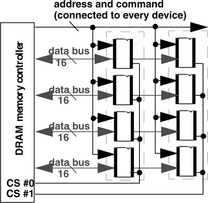
FIGURE 9.33 Typical topology of commodity DRAM memory systems such as DDRx SDRAm. Address and command busses are connected to every device.
The difference in the loading characteristics means that signals propagate far slower on the command and address bus than on the data bus in a typical commodity DRAM memory system. To alleviate the constraints placed on timing by the large number of loads on the command and address busses, numerous strategies have been deployed in modern DRAM memory systems. One strategy to alleviate timing and signaling constraints on the command and address buses is to make use of buffered or registered memory modules. For example, registered dual in-line memory modules (RDIMM) use separate buffer chips on the memory module to buffer command and address signals from the memory controller to the DRAM devices. Figure 9.35 illustrates that, from the perspective of the DRAM memory controller, the signal delivery path is limited to the system board through the socket interface and up to the input of the buffer chips on the memory modules. The buffer chips then drive the signal to the DRAM devices in a separate transmission line. The benefits of the buffer devices in the registered memory modules are shorter transmission lines, fewer electrical loads per transmission line, and fewer transmission line segments. The drawbacks of the buffer devices in the registered memory modules are higher cost associated with the buffer devices and the additional latency required for the address and command signal buffering and forwarding.
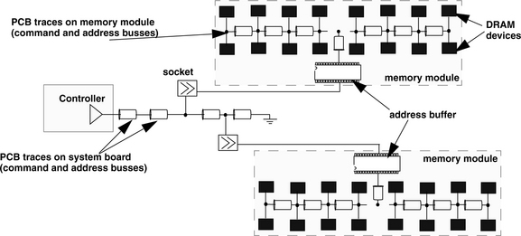
FIGURE 9.35 Register chips buffer command, control, and address signals in a Registered memory system.
9.6.1 Data Read and Write Timing in DDRx SDRAM Memory Systems
Figure 9.33 illustrates that the command and address busses in a commodity DRAM memory system are typically more heavily loaded than the data bus, and timing margins are tighter on the command and address busses when compared to the data bus. Modern DDRx SDRAM memory systems capitalize on the lighter loading characteristics of the data bus by operating the data bus at twice the data rate as the command and address busses. The difference in operating the various busses at different data rates as well as the difference between the role of the DRAM memory controller and the commodity DRAM devices introduces several interesting aspects in the timing and synchronization of DDRx SDRAM devices. Figure 9.36 illustrates several interesting aspects of data read and write timing in commodity DDRx SDRAM devices: the use of a Data Strobe Signal (DQS) in DDRx SDRAM memory systems as the source-synchronous timing reference signal on the data bus, the transmission of symbols on half clock cycle boundaries on the data bus as opposed to full clock cycle boundaries on the command and address busses, and the difference in phase relationships between read and write data relative to the DQS signal.
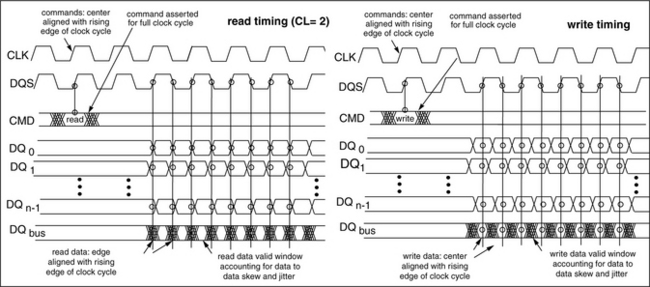
First, Figure 9.36 illustrates that in DDRx SDRAM memory systems, address and command signals are asserted by the memory controller for a full clock cycle, while symbols on the data bus are only transmitted for half cycle durations. The doubling of the data rate on the data bus is an effective strategy that significantly increases bandwidth of the memory system from previous generation SDRAM memory systems without wholesale changes in the topology or structure of the DRAM memory system. However, the doubling of the data rate, in turn, significantly increases the burden on timing margins on the data bus. Figure 9.36 illustrates that valid data windows on the command, address, and data busses are constrained by the worst-case data skew and data jitter that exist in wide, parallel busses. Typically, in a DDRx SDRAM memory system with a 64-bit-wide data bus, the data bus is divided into smaller groupings of 8 signals per group, and a separate DQS signal is used to provide timing reference for each group of data bus signals. In this manner, the amount of timing budget allocated to account for skew and jitter is minimized on a group-by-group basis. Otherwise, much larger timing budgets would have to be allocated to account for skew and jitter across the entire width of the 64-bit-wide data bus. Figure 9.23 illustrates that where the timing budget devoted to tskew increases, tcycle must be increased proportionally, resulting in lower operation frequency.
Figure 9.36 also shows that read and write data are sent and received on different phases of the DQS signal in DDRx SDRAM memory systems. That is, DRAM devices return data bursts for read commands on each edge of the DQS signal. The DRAM memory controller then determines the centers of the valid data windows and latches in data at the appropriate time. In contrast, the DRAM memory controller delays the DQS signal by 90° relative to write data. The DRAM devices then latch in data relative to each edge of the DQS signal without shifting or delaying the data. One reason that the phase relationship between the read data and the DQS signal differs from the phase relationship between write data and the DQS signal is that the difference in the phase relationships shifts the burden of timing synchronization from the DRAM devices and places it in the DRAM memory controller. That is, the commodity DDRx SDRAM devices are designed to be inexpensive to manufacture, and the DRAM controller is responsible for providing the correct phase relationship between write data and the DQS signal. Moreover, the DRAM memory controller must also adjust the phase relationship between read data and the DQS signal so that valid data can be latched in the center of the valid data window despite the fact that the DRAM devices place read data onto the data bus with the same phase relative to the DQS signal.
9.6.2 The Use of DLL in DDRx SDRAM Devices
In DDRx SDRAM memory systems, data symbols are, in theory, sent and received on the data bus relative to the timing of the DQS signal as illustrated in Figure 9.30, rather than a global clock signal used by the DRAM memory controller. Theoretically, the DQS signal, in its function as the source-synchronous clocking reference signal, operates independently from the global clock signal. However, where the DQS signal does operate independently from the global clock signal, the DRAM memory controller must either operate asynchronously or devote additional stages to buffer read data returning from the DRAM devices. A complete decoupling of the DQS signal from the global clock signal is thus undesirable. To mitigate the effect of having two separate and independent clocking systems, on-chip DLLs have been implemented in DDR SDRAM devices to synchronize the read data returned by the DRAM devices, the DQS signals, and the memory controller’s global clock signal. The DLL circuit in a DDR DRAM thus ensures that data returned by DRAM devices in response to a read command is actually returned in synchronization with the memory controller’s clock signal.
Figure 9.37 illustrates the use of an on-chip DLL in a DDR SDRAM device, and the effect that the DLL has upon the timing of the DQS and data signals. The upper diagram illustrates the operation of a DRAM device without the use of an on-chip DLL, and the lower diagram iillustrates the operation of a DRAM device with the use of an on-chip DLL. Where the DRAM device operates without an on-chip DLL, the DRAM device internally buffers the global clock signal and uses it to generate the source-synchronous DQS signal and return data to the DRAM memory controller relative to the timing of the buffered clock signal. However, the buffering of the clock signal introduces phase delay into the DQS signal relative to the global clock signal. The result of the phase delay is that data on the DQ signal lines is aligned closely with the DQS signal, but can be significantly out of phase alignment with respect to the global clock signal.

The lower diagram in Figure 9.37 illustrates that where the DRAM device operates with an on-chip DLL, the DRAM device also internally buffers the global clock signal, but the DLL then introduces more delay into the DQS signal. The net effect is to delay the output of the DRAM device by a full clock cycle so that the DQS signal along with the DQ data signals becomes effectively phase aligned to the global clock signal.
9.6.3 The Use of PLL in XDR DRAM Devices
In an effort devoted to the pursuit of high bandwidth in DRAM memory systems, the Rambus Corp. has designed several different clocking and timing synchronization schemes for its line of DRAM memory systems. One scheme utilized in the XDR memory system involves the use of PLLs in both the DRAM devices and the DRAM memory controller. Figure 9.38 abstractly illustrates an XDR DRAM device with two data pin pairs on the data bus along with a differential clock pin pair. The figure shows that the signals in the XDR DRAM memory system are transported via differential pin pairs. Figure 9.38 further illustrates that a relatively low system clock signal that operates at 400 MHz is used as a global clock reference between the XDR DRAM controller and the XDR DRAM device. The XDR DRAM device then makes use of a PLL to synchronize data latch operations at a higher data rate relative to the global clock signal. Figure 9.38 shows that the use of the PLL enables the XDR DRAM device to synchronize the transportation of eight data symbols per clock cycle. Moreover, the XDR DRAM controller contains a set of adjustable delay elements labelled as FlexPhase. The XDR DRAM memory controller can set the adjustable delay in the FlexPhase circuitry to effectively remove timing uncertainties due to signal path length differentials. To some extent, the FlexPhase mechanism can also account for drift in skew characteristics as the system environment changes. The XDR memory controller can adjust the delay specified by the FlexPhase circuitry by occasionally suspending data movement operations and reinitializing the FlexPhase adjustable delay setting based on the transportation of predetermined test patterns.

9.7 Summary
This chapter covers the basic concepts of a signaling system that form the essential foundation for data transport between discrete devices. Specifically, the physical requirements of high data rate signaling in modern multi-device DRAM memory systems directly impact the design space of system topology and memory-access protocol. Essentially, this chapter illustrates that the task of transporting command, address, and data between the DRAM memory controller and DRAM devices becomes more difficult with each generation of DRAM memory systems that operate at higher data rates. Increasingly, sophisticated circuitry such as DLLs and PLLs is being deployed in DRAM devices, and the desire to continue to increase DRAM memory system bandwidth has led to restrictions to the topology and configuration of modern DRAM memory systems.
1The Telegrapher’s Equations were first derived by William Thomson in the 1850s in his efforts to analyze the electrical characteristics of the underwater telegraph cable. Their final form, shown here, was later derived by Oliver Heaviside.
2The conductive element G is assumed to be much smaller than jωC.
3The frequency of interest here is not the operating frequency of the signals transmitted in DRAM memory systems, but the high-frequency components of the signals as they transition from one state to another.
4In this case, the load is the receiver of the signal.
5SOJ stands for Small Outline J-lead, and TSOP stands for Thin Small Outline Package. Due to their proliferation, these packages currently enjoy cost advantages when compared to Ball Grid Array (BGA) type packages.
6DDR SDRAM was originally only specified with speed bins up to 166 MHz at a supply voltage level, Vddq, of 2.5 V. However, market trends and industry pressure led to the addition of the 200-MHz (400-Mbps) speed bin in DDR SDRAM memory systems. The 200-MHz DDR SDRAM memory system is specified to operate with a supply voltage, Vddq, of 2.6 V.
7DDRx denotes different generations of SDRAM devices such as DDR SDRAM, DDR2 SDRAM, and DDR3 SDRAm. Similarly, GDDRx denotes different generations of GDDR devices such as GDDR2 and GDDR3.
8Logic based, as opposed to memory based.