
Scanning Probe and Particle Beam Microscopy
Alexandre Cuenat and Richard Leach, National Physical Laboratory
This chapter introduces scanning probe and particle beam measurement techniques. After a short introduction to scanning probe microscopy, the most popular techniques are presented in detail: scanning tunnelling microscopy and atomic force microscopy. Noise sources and imaging artefacts in atomic force microscopy are addressed, followed by traceability and calibration techniques. Force measurement with atomic force microscopy is then discussed and methods for cantilever calibration. Use of atomic force microscopy for measuring nanoparticles is covered along with other modes of probe microscopy. Electron microscopy is discussed in detail, both scanning and transmission modes, and calibration. The chapter finishes by discussing alternative particle beam techniques such as focussed and helium ion microscopy.
Keywords
Scanning Probe Microscopy; Scanning Tunnelling Microscopy; Atomic Force Microscopy; Cantilever Calibration; Nanoparticles Measurement; Scanning Electron Microscopy; Transmission Electron Microscopy
As technology moves deeper into the realm of the microscopic by manufacturing smaller components, it becomes essential to measure at a suitable scale and resolution. For an increasing range of technologies, the relevant scale is the nanometre. In this case, a resolution of the order of a few atomic distances or even smaller is expected. In the late seventeenth century, the development of optical microscopes enabled scientists to observe structure on the scale of micrometres, and until the twentieth century, the optical microscope was the fundamental instrument that enabled imaging in materials and biological sciences. However, the observation of single atoms or sub-micrometre details requires far more resolution than (far field) visible light can provide.
At the start of the twentieth century, the electron microscope was developed based on the newly discovered wave-like properties of the electron. Indeed, electrons with sufficient energy will have a wavelength comparable to the diameter of an atom or smaller. Unfortunately, electron optics limit the resolution that an electron microscope can reach and true atom-by-atom resolution is far from routine.
A study of surface atoms is even more challenging and requires a different type of probe because high-energy electrons will penetrate into the bulk material without providing surface information, while low-energy electrons will be scattered by the surface. For many years, scientists have used diffraction phenomena to study the atomic ordering at surfaces, but the lateral resolution is of the order of a micrometre.
The development of the scanning tunnelling microscope (STM) by Gerd Binnig and Heinrich Rohrer in 1982 [1] was a major step in the development of a new area of technology – nanotechnology. The STM enabled the next step in imaging and probing technology by providing direct images of the atoms at the surface of a sample. The STM may not have been the first scanning probe system, but the atomic resolution it demonstrated captured the imagination of the scientific community. One of the key aspects of STM is the very close proximity of the probe with the sample – usually a few nanometres or less; this type of technique is called a near-field technique. Since the invention of the STM, a series of near-field methods have been developed, capable of probing or imaging many physical or chemical properties with nanometre-scale resolution. All these microscopes are based on the same principle: a very sharp tip, with a radius typically of a few nanometres, is scanned in close proximity to a surface using a piezoelectric scanner. The much localised detection of forces in the near field is in marked contrast with previous instruments, which detected forces over much larger areas or used far-field wave phenomena.
This chapter reviews the principal methods that have been developed to measure properties at the nanoscale and the related metrology challenges, with a particular focus on the atomic force microscope (AFM). The reason for this choice is that the AFM is by far the most popular instrument to date and is the most likely candidate to be fully traceable – including force – in the near future. Electron microscopes, scanning and transmission, are also included in this chapter as they are capable of giving information in the same range and are also very popular. The use of electron microscopes, however, is somewhat limited to dimension and some chemical information. This chapter concludes with a few words on the focused ion beam (FIB) microscope and the newly developed helium ion microscope.
7.1 Scanning probe microscopy
Scanning probe microscopes (SPMs) are increasingly used as quantitative measuring instruments not only for dimensions but also for physical and chemical properties at the nanoscale (see Refs. [2,3] for thorough introductions to SPM technology). Furthermore, SPM has recently entered the production and quality-control environment of semiconductor manufacturers. However, for these relatively new instruments, standardised calibration procedures still need to be developed.
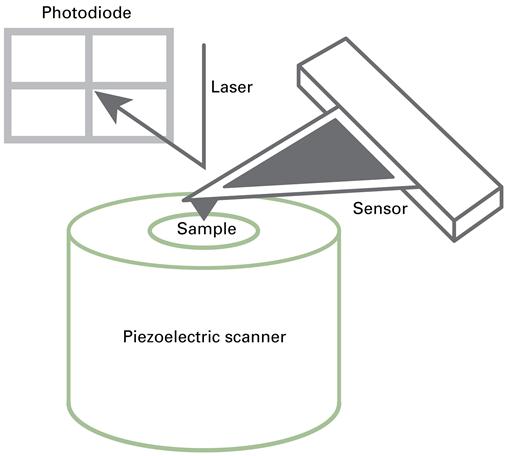
From an instrumentation perspective, the SPM is a serial measurement device, which uses a nanoscale probe to trace the surface of the sample based on local physical interactions (in a similar manner to a stylus instrument – see Section 6.6.1). While the probe scans the sample with a predefined pattern, the signal of the interaction is recorded and is usually used to control the distance between the probe and the sample surface. The presence of a feedback mechanism based on a detected force and the scanning of a nanoscale probe form the basis of all scanning probe instruments. Figure 7.1 is a schema of an AFM; a sample is positioned on a piezoelectric scanner, which moves the sample in three dimensions relative to a transduction mechanism (in this case a flexible mechanical cantilever) with a very sharp tip in very close proximity to the sample.
Depending on the physical interactions used to probe the surface, the system can have different names, for example:
• STMs are based on the quantum-mechanical tunnelling effect (see Section 7.2);
• AFMs use inter-atomic or inter-molecular forces (see Section 7.3); and
• scanning near-field optical microscopes (SNOMs) probe the surface using near-field optics (see Refs. [2,4]).
Based on these three core concepts, a large variety of SPM methods have been developed that use almost every known physical forces: electrostatic, magnetic, capacitive, chemical and thermal. It is, however, customary to separate all these methods into two larger groups, depending on the force measured for the feedback mechanisms:
Contact mode: the probe is in permanent contact with the surface, that is usually a repulsive force between the tip and the sample is used as feedback to control the distance between the tip and the sample.
Non-contact mode: the probe oscillates slightly above the surface, and the interactions with the sample surface forces modify the oscillation parameters. One of the oscillation parameters (amplitude, frequency or phase shift) is kept constant with the feedback loop, while the others are monitored for measurement purpose.
Intermittent mode: non-contact mode in which the probe oscillates with a high amplitude and touches the sample for a short time (often referred to as tapping mode).
7.2 Scanning tunnelling microscopy
As its name suggests, the STM takes advantage of the quantum-mechanical phenomenon of tunnelling. When an electron approaches a potential energy barrier higher than the electron energy, the electron is not completely reflected as one would expect classically, but rather the electron wavefunction exponentially decays as it travels through the barrier. With a sufficiently thin barrier, there is a small but non-negligible probability that the electron can be found on the other side of the barrier. In practice, the STM is built around the precise scanning of an ultra-sharp conductive tip close to a conductive sample biased with a small potential difference compared to the tip. The electron probability densities of the tip and the substrate can overlap if the distance between the two is small enough; in which case the application of a potential difference between the tip and the sample results in a current due to the electrons tunnelling through the insulating gap formed by the vacuum layer between the tip and the substrate. This tunnelling current is exponentially sensitive to the distance between the tip and the sample. With a barrier height (work function) of a few electron volts, a change in distance by an amount equal to the diameter of a single atom (approximately 0.2 nm) causes the tunnelling current to change by up to three orders of magnitude [1]. The key technology that has enabled the STM, and subsequent scanning probe systems, to be developed is the ability to move the tip by a controlled amount with a resolution of a few picometres. This is possible using piezoelectric materials, which move the tip over the sample as well as scanning the substrate.
In the original mode of operation, the feedback will control the piezoelectric actuator in the z-direction in order to maintain a constant tunnelling current, by keeping the tip at a constant height relative to the surface. With this constant current method, a topographical map of a surface is obtained. However, this procedure will yield purely topographical information only when used on an electronically homogeneous surface; when applied to an electronically inhomogeneous surface, the tunnelling current will depend on both the surface topography and the local electronic structure. For example, if the effective local tunnelling barrier height increases or decreases at a point on the surface, then the feedback system must decrease or increase the tip–sample separation in order to maintain a constant tunnelling current. The final image obtained will thus contain electronic structure information convoluted with the topographical information. A solution to this problem is the so-called barrier-height imaging mode [5] used to measure varying work function (tunnelling barrier height) over inhomogeneous samples. In this mode, the tip is scanned over each measurement site and the distance between the tip and the sample is varied while recording dI/dz; the rate of tunnelling current, I, changes with respect to tip–sample distance, z. From this information, the work function at each location can be determined and used to correct the constant current measurement. One of the main limitations of STM is that it can be used only with conductive samples.
7.3 Atomic force microscopy
The AFM [6,7] was developed to image insulating surfaces with atomic resolution. AFM is the most widely used member of the family of SPM techniques. Its versatility and the availability of a number of commercial instruments make it a method of choice for research laboratories, from academia to industry.
Figure 7.2 is a schematic of a standard AFM (it is in fact representative of most SPM types). An AFM’s essential components are as follows:
• deflection detector, for example optical beam deflection method, piezoresistive sensor [8] or Fabry–Pérot fibre interferometer [9]; and

The sample is scanned continuously in two axes (xy) underneath a force-sensing probe consisting of a tip that is attached to, or part of, a cantilever. A scanner is also attached to the z-axis (height) and compensates for changes in sample height or forces between the tip and the sample. The presence of attractive or repulsive forces between the tip and the sample will cause the cantilever to bend and this deflection can be monitored in a number of ways. The most common system to detect the bend of the cantilever is the optical beam deflection system, wherein a laser beam reflects off the back of the cantilever onto a photodiode detector. Such an optical beam deflection system is sensitive to sub-nanometre deflections of the cantilever [10].
7.3.1 Noise sources in atomic force microscopy
The limitations of the metrological capabilities of an AFM due to thermal noise are well documented [11]. However, not only thermal but all noise sources need to be systematically investigated and their particular contributions to the total amount of the noise quantified for metrological purposes [12]. Note that most of the discussions on noise in AFM are also of relevance to other forms of SPM.
Noise sources can be either external, including:
• variations of temperature and air humidity – these will usually fix an absolute limit for the accuracy of the method;
• air motion (e.g. air conditioning, air circulation, draughts, exhaust heat);
• mechanical vibrations (e.g. due to structural vibrations, pumps – see Section 3.9); and
• acoustic (e.g. impact sound, ambient noise – see Section 3.9.6).
or internal (intrinsic), including:
In practice, state-of-the-art AFMs in metrology laboratories have a resolution limited only by the temperature of the measurement. There are unfortunately no general calibration artefacts able to test this level of resolution for all AFM methods. Force and lateral resolution, as well as the overall accuracy of measurement, should be approached with caution in the absence of a clearly identified method to measure them.
It is well known that adjustments made by the user (e.g. the control loop parameters, scan field size and speed) also have a substantial influence on the measurement [13].
To reduce the total noise, the sub-components of noise must be investigated. The total amount of the z-axis noise can be determined by static or dynamic measurements [14] as described in the following section.
7.3.1.1 Static noise determination
To determine the static noise of an SPM, the probe is placed in contact with the sample, the distance is actively controlled, but the xy scan is disabled, that is the scan size is zero. The z-axis signal is recorded and analysed (e.g. root mean square (RMS) determination or calculation of the fast Fourier transform to identify dominant frequencies, which then serve to identify causes of noise). An example of a noise signal for an AFM is shown in Figure 7.3; the RMS noise is 13 p.m. in this case (represented as an Rq parameter – see Section 8.2.7.2).

7.3.1.2 Dynamic noise determination
To determine the dynamic noise of an SPM, the probe and sample are displaced in relation to one another (line or area scan). In this case, scan speed, scan range and measurement rate should be set to values typical of the subsequent measurements to be carried out. Usually the dynamic noise measurement is carried out at least twice with as small a time delay as possible. The calculation of the difference between the subsequent images is used to correct for surface topography and guidance errors inherent in the scanner.
7.3.1.3 Scanner xy noise determination
The accurate determination of xy noise is extremely difficult for AFM as they have small xy position noise and thus require samples with surface roughness substantially smaller than the xy noise [12]. In individual cases, the noise of sub-components can be determined. For the xy stage, for example, the xy position noise can be measured with a laser interferometer.
For AFM, the following guidance deviations are usually observed:
• out-of-plane motions or scanner bow, that is any form of crosstalk of xy movements to the z-axis;
• line skips in the z-direction;
• distortions within the xy-plane (shortening/elongation/rotation) due to orthogonality and/or angular deviations; and
• orthogonality deviations between the z- and the x- or y-axis.
Guidance deviations can be due to the design and/or be caused by deviations in the detection or control loop. Guidance deviations show a strong dependence on the selected scan field size and speed, as well as on the working point in the xy-plane and within the z-range of the scanner. When the reproducibility is good, such systematic deviations can be quantified and corrected for by calibration.
7.3.2 Some common artefacts in AFM imaging
One of the reasons that AFMs only been integrated into the production environment in a few specialised applications is the presence of numerous ‘artefacts’ in their images that are not due to the surface topography of the surface being measured. Usually a high level of expertise is required to identify these artefacts. The availability of reference substrates and materials will allow industry to use AFMs (and other SPMs) more widely.
7.3.2.1 Tip size and shape
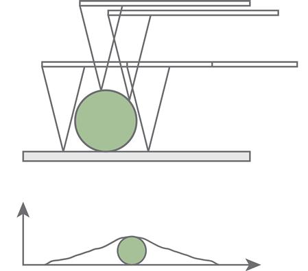
Many of the most common artefacts in AFM imaging are related to the finite size and shape of the tip. Commonly used AFM probes, such as those manufactured from silicon nitride and silicon, have pyramidal-shaped tips [15]. These tips can have a radius of curvature as small as 1 nm, but often the radius is much larger. When imaging vertical features that are several tens of nanometres or more in height, the tip half angle limits the lateral resolution. When the tip moves over a sharp feature, the sides of the tip, rather than just the tip apex, contact the edges of the feature (Figure 7.4). For features with vertical relief less than approximately 30 nm, it is the radius of curvature of the tip that limits resolution, resulting in tip broadening of the feature of interest. The resulting image is a non-linear combination of the sample shape and the tip shape. Various deconvolution (or its non-linear equivalent, erosion) methods, including commercial software packages, are available although such software must be used with caution [16–18]. There are also many physical artefacts that can be used to measure the shape of an AFM tip [19–21].
7.3.2.2 Contaminated tips
An ideal AFM tip ends in a single point at its apex. However, manufacturing anomalies and/or contamination may lead to double or even multiple tip ends. When this occurs, the tips can map features on the sample surface more than once. For example, a double tip will result in a regular doubling of features. Such artefacts lead to what are commonly termed double- or multiple-tip images. Contaminants on a tip can also interact with a sample surface, leading to repeated patterns of the contaminants scattered across the surface. Cleaning of AFM tips and cantilevers is highly recommended [22].
7.3.2.3 Other common artefacts
When the gain parameter of the control loop is too high, rippling artefacts can occur along the edges of features. These ripples tend to occur along the leading edge of a feature and will generally switch position when the scan direction is changed. Shadow artefacts generally occur along the trailing edge of a feature, when the feedback loop is unable to compensate for a rapid change in topography. Reducing the scan speed often minimises shadow artefacts. Sample damage or deformation during scanning is also a significant artefact, particularly for soft surfaces.
Piezoelectric and/or thermal drift can distort images, particularly at the start of scanning. Measuring near to the centre of the z-axis piezoelectric actuator’s range, and allowing the AFM and the sample to sit for a period to reach thermal equilibration, can substantially improve drift-related problems.
7.3.3 Determining the coordinate system of an AFM
There will always be some imperfections in the coordinate system for a given AFM. The calibration of the lateral scan axes is usually carried out using 1D or 2D lateral calibration artefacts. These artefacts are usually formed by equidistant structures with defined features whose mean spacing (the pitch) serves to calibrate the lateral axes. In Figure 7.5(a), a set of parallel regression lines along similar features of the structure is calculated. The mean distance between these lines is the pitch, px. In Figure 7.5(b), a set of parallel regression lines is calculated, each through a column of centres of similar features; the mean distance between these lines is the pitch, px in the x-direction of the grating. Similarly, another set of parallel regression lines is calculated, each through a series of centres of the grating; the mean distance of these grating lines is the pitch, py in the y-direction of the grating. The orthogonality of the grating is the angle formed by the px and py vectors.

Local deviations are a measure of the non-linearity of the axes. In addition, the orthogonality deviation and the crosstalk of the lateral scan axes can be determined.
For 2D lateral artefacts, it is important not to confuse the pitches, px and py, and the mean spacings, ax and ay, of the individual grating: px and ax or py and ay are identical only for perfectly orthogonal gratings. Where high-quality gratings are used, which are almost orthogonal, the difference can often be ignored in the calibration of the axes. These differences, however, become significant when a 2D artefact is used to check the orthogonality of the scanner axes.
In measurements on lateral artefacts, the selection of the scan range and the scan speed or rate is important, because the calibration factors are strongly influenced by dynamic non-linearity and image distortions [23]. This is also true for systems with active position control. In calibration, the scan speed must, therefore, be adjusted to reflect the later measurements that are to be made.
7.3.4 Traceability of atomic force microscopy
From the metrological point of view, AFMs are generally subdivided into the three categories [12]:
1. Reference AFMs with integrated laser interferometers allowing direct traceability of the axis scales, via the wavelength of the laser used, to the SI unit of length (often referred to as metrological AFMs, see Refs. [24–27] for examples developed at National Measurement Institutes).
2. AFMs with position measurement using displacement transducers, for example capacitive or inductive sensors, strain gauges or optical encoders. These sensors are calibrated by temporarily mounting laser interferometers to the device or by measuring high-quality calibration artefacts. Two types are to be distinguished here:
a. active position control AFMs that track to scheduled positions by means of a closed-loop control system; and
b. AFMs with position measurement but without closed loop for position control (open loop systems).
3. AFMs in which the position is determined from the electrical voltage applied to the piezoelectric scanners and, if need be, corrected using a look-up table. Such AFMs need to be calibrated using a transfer artefact that has itself been calibrated using a metrological AFM (highest accuracy) or an AFM with position measurement. These instruments will, however, suffer from hysteresis in the scanner.
Another important aspect of traceability is the uncertainty of measurement (see Section 2.8.3). It is very rare to see AFM measurements quoted with an associated uncertainty as many of the points discussed in Section 6.11 apply to AFMs (and SPMs in general). Uncertainties are usually only quoted for the metrological AFMs or for simple artefacts such as step heights [28] or 1D gratings [29].
7.3.4.1 Calibration of AFMs
Calibration of AFMs is carried out using certified reference artefacts. Suitable sets of artefacts are available from various manufacturers (see www.nanoscale.de/standards.htm for a comprehensive list of artefacts). An alternative is to use laser interferometers to calibrate the axes, which offer a more direct method to traceability if frequency-stabilised lasers are used.
The aim of the calibration is the determination of the axis scaling factors, Cx, Cy and Cz. Apart from these scaling factors, a total of t21 sources of geometrical error can be identified for the motion process of the SPM, similar to a CMM operating in 3D (see Section 9.2).
A typical calibration for an AFM proceeds in the following manner [12]:
• the crosstalk of lateral scan movements to the z-axis is investigated by measurements on a flatness artefact;
• the crosstalk of the lateral scan axes and the orthogonality deviation is determined using a 2D lateral artefact. This artefact is usually used to calibrate Cx and Cy;
• deviations from orthogonality can be determined using artefacts with orthogonal structures; and
• orthogonality deviations are measured using 3D artefacts. Calibration of the z-axis, Cz, and deviations are achieved using 3D artefacts.
In most cases, different artefacts are used for these calibration steps (Table 7.1). Alternatively, 3D artefacts can be used – with suitable evaluation software – to calibrate all three factors, Cx, Cy and Cz, and the crosstalk between all three axes.
Table 7.1
Overview of Guidance Deviations, Transfer Artefacts to Be Used and Calibration Measurements [12]
| Calibration | Artefact Required | What Is Measured? |
| Crosstalk of the lateral movements to the z-axis | Flatness artefact | Out-of-plane movement of xy scan system |
| Orthogonality deviation | 2D artefact | Angle formed by the two axes, on orthogonal structures |
| 3D artefact | Need description of what is measured for a 3D artefact | |
| Cx and Cy deviations(non-linearities) | 1D or 2D lateral artefact | Pitch measurement, rotation, linearity |
| Crosstalk of the lateral axes | 2D lateral artefact | Pitch measurement, rotation, linearity |
| Cz deviations (non-linearities) | Step height artefact | Step height measurement, linearity |

7.3.5 Force measurement with AFMs
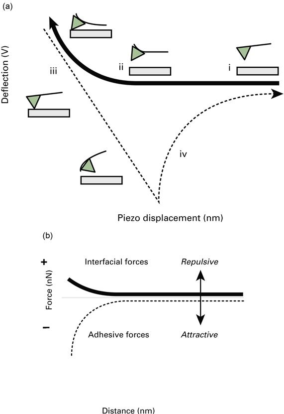
Force measurements with an AFM are carried out by monitoring the cantilever deflection as the sample approaches, makes contact with, and then retracts from the cantilever. However, the raw cantilever deflection measurement is a measure of the deflection of the cantilever at some point and not directly of the force. For a beam deflection system, for example, the cantilever deflection is recorded in volts. An additional problem is that the distance (or separation) between the tip and the sample is not measured directly [30]; the AFM measures the displacement of the piezoelectric scanner that supports the sample. A force curve graph of cantilever deflection (in volts) and corresponding piezoelectric scanner displacement (in metres) (Figure 7.6(a)) must be interpreted to give a force–distance curve (i.e. force of interaction in units of force against separation between the sample and the cantilever in units of length (see Figure 7.6(b))). With reference to Figure 7.6(a), when the tip and sample are far apart (i) they exhibit no interaction (zero force). As the sample approaches the tip, inter-molecular forces between the tip and the sample cause the cantilever to deflect upwards (ii) due to repulsive forces (in this case between a charged substrate and tip, but attractive forces are commonly observed as well). Eventually the tip makes contact with the sample (iii) and their movement becomes coupled (region of constant compliance). The sample is then retracted from the tip (iv) until the tip/cantilever and sample return to their original positions completing one cycle. Hysteresis, shown here, may occur upon retraction due to adhesion forces. Interfacial forces are measured on approach and adhesion forces are measured upon retraction; repulsive forces are positive and attractive forces are negative.
To obtain the force part of the force–distance curve, the photodiode values are converted to force using F=kcd, where F is the force, d is the cantilever deflection and kc is the cantilever spring constant. To convert the cantilever deflection measured by the photodiode in volts to metres, a displacement conversion factor (also called the optical lever sensitivity) is obtained from the region of the force curve where the sample is in contact with the cantilever. For an infinitely hard contact, every displacement of the piezoelectric scanner displaces the sample or the tip; the cantilever is pushed upwards, which is recorded as a voltage output on the photodiode. The slope of the force curve in the region where the cantilever is in contact with the sample defines the optical lever sensitivity. This part of the force curve is called the region of constant compliance or region of contact.
It is important to note that using the constant compliance region of the force curve to convert photodiode response to deflection will overestimate the force of interaction if the cantilever is not the most compliant component of the system. This is often the case when soft, deformable substances such as polymers are used in force measurements (either as a sample or linked to the tip/cantilever). If a compliant substrate is used, other methods are needed to accurately convert the measured deflection of the cantilever into a force of interaction [31]. In this case, the optical lever sensitivity is determined by pressing the tip/cantilever against a hard sample (e.g. mica), before and after it is used on a soft sample. However, often this method does not work as the optical lever sensitivity is strongly dependent upon a number of factors. These factors include the position and shape of the laser spot and the difficulty in precisely aligning the laser spot on the same position on the cantilever from experiment to experiment. Also, the use of a hard sample cannot be applied if it is the tip/cantilever that supports the most compliant component of the system (e.g. a molecule attached to the cantilever). Another method that relies on the ‘photodiode shift voltage’, a parameter that is very sensitive to the position and shape of the laser of the photodetector, can be used to convert volts of cantilever deflection into metres of deflection [32]. This method ensures that forces can be determined regardless of the compliance of the cantilever relative to any other component in the AFM, and also ensures the preservation of fragile macromolecules, which may be present on the sample or attached to the cantilever.
7.3.6 AFM cantilever calibration
AFMs are sensitive to very small forces in the piconewton range. In order to measure these forces accurately, the stiffness of the probe must be determined. Stiffness calibration procedures rely on imposing known forces on the probe, measuring the geometrical and material properties of the probe, or measuring its thermal fluctuations.
The cantilever’s spring constant is essentially dependent upon its composition and dimensions [33]. Nominal values listed by manufacturers may be incorrect by an order of magnitude and it is, therefore, necessary to determine the spring constant for each cantilever or for each batch of cantilevers from a wafer [34]. Parameters such as Young’s modulus (related to composition), and cantilever length and thickness, can be used with theoretical equations to calculate a spring constant [35]. However, calculated values can be inaccurate due to the unknown material properties of the cantilever (the stoichiometry of silicon nitride, for example, can vary from Si3N4 to Si5N4 [36]). Furthermore, the measurement of cantilever thickness, which is a dominant parameter in theoretical equations, is extremely difficult. The spring constant depends on the cantilever thickness to the third power, so even small uncertainty in the thickness measurement will result in large variations in the calculated spring constant [37].
An accurate, but often destructive, way to measure spring constant is the added-mass method [38]. In this method, beads of known mass are attached to the end of the cantilever. The additional mass causes the cantilever resonant frequency to decrease proportional to the mass. A graph of added mass against resonant frequency yields a straight line with a slope corresponding to the spring constant.
A further method to determine the spring constant is the measurement of the force that an AFM imparts onto a surface by measuring the thermal fluctuations of the cantilever – in this method, the cantilever is modelled as a simple harmonic oscillator (usually only in one degree of freedom) [39]. With knowledge of the potential energy of the system and applying the equipartition theorem, the spring constant of the cantilever can be calculated from the motion of the cantilever and its surrounding heat-bath temperature. The thermal method has three major problems [40]: (i) higher vibration modes cannot be ignored, (ii) the method to measure deflection usually measures the inclination rather than the displacement and (iii) only the first modes are accessible due to the bandwidth limitations of the experiments.
For directly traceable measurements of the force an AFM cantilever imparts on a surface, electrostatic balances can be used, but they are very costly and inconvenient (see Section 10.3.3). Many of the devices discussed in Section 10.3.4 can also be used to measure spring constant when used as passive springs.
7.3.7 Inter- and intra-molecular force measurement using AFM
As discussed previously, the AFM images a sample by sensing and responding to forces between the tip and the sample. Because the force resolution of the AFM is so sensitive (0.1–1 pN), it is a powerful tool for probing the inter- and intra-molecular forces between two substances. Researchers have taken advantage of this sensitivity to quantify fundamental forces between a sample and some substance linked to the AFM cantilever or tip [41]. The AFM has enabled some truly remarkable advances in the physical sciences due to the sensitivity and ranges of force it can measure. A few examples will be discussed here. A basic understanding of the forces between the AFM tip and the sample is essential for a proper use of the instrument and the analysis of the data. A variety of forces that come into play between the tip and the sample are summarised in Table 7.2. The discussion that follows will focus on contact-mode AFM, which is the most commonly used imaging mode. A recent review highlights the effect of surface forces on dimensional measurements [30].
Table 7.2
Examples of Surface Forces Commonly Encountered in AFM Measurement
| Type of Force | Dependence of Energy on Distance (d) | Energy (kJ·mol−1) | Range (nm) |
| Intra-molecular (ionic or covalent) | 1/d | 100s | <1 |
| London dispersion | 1/d6 | 1–3 | 0.5–5 |
| H-bonding | 1/d3 | 15–20 | 0.5–3 |
| Dipoles | 1/d3 | 5–10 | 0.5–3 |
| Electrostatic | e−d | 10–100 | 10s–100s |
| Van der Waals | 1/d | 1–5 | 5–10 |
| Solvation | ~e−d | 1–10 | <5 |
| Hydrophobic | ~e−d | 1–5 | 10s–100s |

The total force between the tip and the sample results from the sum of various attractive and repulsive forces. As a model, consider the Lennard-Jones potential, which describes the change in inter-molecular potential energy (ϕ) that occurs as two particles, such as atoms or molecules (on tip and sample), are brought closer together. The model gives
(7.1)
where σ is approximately the atomic or molecular diameter (distance of closest approach), ɛ is the minimum value of the potential energy, or the depth of the potential energy well, and r is the separation distance [42]. As the particles are brought closer together from relatively distance separations, the (1/r)6 term (i.e. Van der Waals term) describes the slow change in attractive forces. As the particles are brought even closer together, the (1/r)12 term describes the strong repulsion that occurs when the electron clouds strongly repel one another.
The Van der Waals interaction forces are long-range, relatively weak attractive forces. The origin of the Van der Waals forces is quantum mechanical in nature; they result from a variety of interactions, primarily induced dipole and quadrupole interactions. The Van der Waals forces are non-localised, meaning that they are spread out over many atoms. Van der Waals forces for a typical AFM have been estimated to be of the order of 10–20 nN [43].
The so-called atomic force (a result of the Pauli exclusion principle) is the primary repulsive force at close approach. The magnitude of this force is difficult to predict without a detailed understanding of surface structure.
Several additional forces or interactions must be considered for an AFM tip and sample surface. Capillary adhesion is an important attractive force during imaging in air. The capillary force results from the formation of a meniscus made up of water and organic contaminants adsorbed on to the surface of the tip and the sample [36] (Figure 7.7). The capillary force has been estimated to be of the order of 100 nN or greater. When the tip and the sample are completely immersed in liquid, a meniscus does not form and the capillary forces are absent. Some tips and samples may have hydrophobic properties, in which case hydrophobic interactions must also be taken into consideration.

Water near hydrophilic surfaces is structured [34]. When the tip and the sample are brought into close contact during force microscopy in solution or humid air, repulsion arises as the structured water molecules on the surfaces of the tip and the sample are pushed away. In aqueous solutions, electrical double-layer forces, which may be either attractive or repulsive, are present near the surfaces of the tip and the sample. These double-layer forces arise because surfaces in aqueous solution are generally charged.
Lateral frictional forces must also be taken into account as the sample is scanned beneath the tip. At low forces, a linear relationship should hold between the lateral force and the force normal (vertical) to the surface with a proportionality constant equal to the coefficient of friction. This relationship is valid up to an approximately 30 nN repulsive force [44]. Frictional forces vary on an atomic scale and with temperature, scan velocity, relative humidity and tip and sample materials.
7.3.7.1 Tip functionalisation
Inter- and intra-molecular forces affect a variety of phenomena, including membrane structure, molecular recognition and protein folding/unfolding. AFM is a powerful tool for probing these interactions because it can resolve forces that are several orders of magnitude smaller than the weakest chemical bond, and it has appropriate spatial resolution. In recent years, researchers have taken advantage of these attributes to create chemical force microscopy [45]. AFM probes (i.e. cantilevers or tips) are functionalised with chemical functional groups, biomolecules or living, fully functional cells to make them sensitive to specific interactions at the molecular to cellular level (Table 7.3).
Table 7.3
Various Substances That Have Been Linked to AFM Tips or Cantilevers
| Substance Linked to Tip/Cantilever | Linkage Chemistry |
| Protein | Adsorption, imide, glycol tether, antibody–antigen |
| Nucleic acid | Thiol |
| Polysaccharide | Adsorption |
| Glass or latex bead | Epoxy |
| Living microbial cell | Silane, poly-lysine |
| Dead microbial cell | Gluteraldehyde |
| Eukaryotic cell | Epoxy, adsorption |
| Organic monolayer | Self-assembling monolayer, silane |
| Nanotube | Epoxy |
There are many ways to functionalise an AFM tip or cantilever. All functionalisation methods are constrained by one overriding principle – the bonds between the tip/cantilever and the functionalising substance (i.e. the forces holding the substance of interest to the tip/cantilever) must be much stronger than those between the functionalising substance and the sample (i.e. the forces that are actually measured by the AFM). Otherwise, the functionalising substance would be ripped from the tip/cantilever during force measurements.
Single, colloidal-size beads, a few micrometres in diameter, can be routinely attached to a cantilever using an epoxy resin [46]. Such beads may be simple latex or silica spheres, or more complex designer beads imprinted with biomolecular recognition sites. Care must be taken to select an epoxy that is inert in the aqueous solution and that will not melt under the laser of the optical lever detection system [47].
Simple carboxylic, methyl, hydroxyl or amine functional groups can be formed by self-assembling monolayers on gold-coated tips [45] or by creating a silane monolayer directly on the tip. Organosilane modification of a tip is slightly more robust because it avoids the use of gold, which forms a relatively weak bond with the underlying silicon or silicon nitride surface of the tip in the case of self-assembling monolayers. Carbon nanotubes (CNTs) that terminate in select functional groups can also be attached to cantilever tips [48]. The high aspect ratio and mechanical strength of CNTs creates functionalised cantilevers with unprecedented strength and resolution capabilities. Direct growth of CNTs onto cantilevers by methods such as chemical vapour deposition [49] will probably make this method more accessible to a large number of researchers.
Biomolecules such as polymers, proteins and nucleic acids have been linked to AFM tips or deposited directly on the cantilever [50]. One of the simplest attachment techniques is by non-specific adsorption between a protein, for example, and silicon nitride. The adsorbed protein can then serve as a receptor for another protein or ligand. Virtually any biomolecule can be linked to a cantilever either directly or by means of a bridging molecule. Thiol groups on proteins or nucleic acids are also useful because a covalent bond can be formed between sulfhydryl groups on the biomolecule and gold coatings on a tip. Such attachment protocols have been very useful; however, there are some disadvantages. The linkage procedure may disrupt the native conformation or function of the biomolecule, for example if the attachment procedure disrupts a catalytic site. It is well known that a protein attached to a solid substrate (a cantilever or tip) may exhibit a significantly different conformation, function and/or activity relative to its native state within a membrane or dissolved in solution. Therefore, care must be taken to design control experiments that test the specificity of a particular biomolecule as it occurs in its natural state.
7.3.8 Tip–sample distance measurement
To obtain the distance or separation part of the force–distance curve, a point of contact (i.e. zero separation) must be defined and the recorded piezoelectric scanner position (i.e. displacement) must be corrected by the measured deflection of the cantilever. Simply adding or subtracting the deflection of the cantilever to the movement of the piezoelectric scanner determines the displacement. For example, if the sample attached to the piezoelectric scanner moves 10 nm towards the cantilever, and the cantilever is repelled 2 nm due to repulsive forces, then the actual cantilever–sample separation changes by only 8 nm. The origin of the distance axis (the point of contact) is chosen as the beginning of the region of constant compliance, that is the point on the force curve where cantilever deflection becomes a linear function of piezoelectric scanner displacement (see Figure 7.6). Just as it was difficult to convert photodiode voltage to displacement units for soft, deformable materials, it is not always easy to select the point of contact because there is no independent means of determining cantilever–sample separation. For deformable samples, the cantilever indents into the sample such that the region of constant compliance may be non-linear and the beginning point cannot be easily defined. Recently, researchers have developed an AFM with independent measurement of the piezoelectric scanner and the cantilever displacements [51].
7.3.9 Challenges and artefacts in AFM force measurements
There are a number of artefacts that have been identified in force curves. Many of these artefacts are a result of interference by the laser, viscosity effects of the solution or elastic properties of soft samples. When the sample and the cantilever are relatively remote from each other, such that there is no interaction, the force curve data should be a horizontal line (i.e. the region of non-contact; see Figure 7.6). However, the laser has a finite spot size that may be larger than the size of the cantilever such that the laser beam reflects off the sample as well as the cantilever. This is particularly troublesome for reflective substrates, often resulting in optical interference, which manifests itself as a sinusoidal oscillation or as a slight slope in the non-contact region of the force curve [52]. This affects the way in which attractive or repulsive forces are defined. A simple solution is to realign the laser on the cantilever such that the beam does not impinge upon the underlying sample. Alternatively, the oscillation artefact may be removed from the force curve with knowledge of the wavelength of the laser. This optical problem has been largely solved in commercial AFMs by using superluminescent diodes, which possess high optical power and low-coherence length.
A further artefact is the hysteretic behaviour between the approach and retraction curves in the non-contact area. The approach and retraction curves often do not overlap in high-viscosity media due to fluid dynamic effects [53]. Decreasing the rate at which the piezoelectric scanner translates the samples towards and away from the cantilever can help to minimise hysteresis by decreasing the drag caused by the fluid.
Another frequently observed artefact in the force curve is caused by the approach and retraction curves not overlapping in the region of contact, but rather being offset laterally. Such artefacts make it difficult to define the point of contact, which is necessary to obtain separation values between the sample and the tip. Such hysteresis artefacts are due to frictional effects as the tip (which is mounted in the AFM at an angle of typically 10°–15° relative to the sample) slides on the sample surface. This hysteresis is dependent upon the scan rate and reaches a minimum below which friction is dominated by stick-slip effects, and above which friction is dominated by shear forces. This artefact may be corrected by mounting the sample perpendicular to the cantilever, thereby eliminating lateral movement of the cantilever on the sample.
Viscoelastic properties of soft samples also make it difficult to determine the point of contact and to measure accurately the forces of adhesion. When the cantilever makes contact with a soft sample, the cantilever may indent the sample such that the region of contact is non-linear. It is then difficult to determine the point at which contact begins. The rate at which the sample approaches or retracts from the tip also affects the adhesive force measured on soft samples. This is because the tip and sample are weakly joined over a large contact area that does not decouple fast enough as the tip is withdrawn at very high scan rates. Thus, the membrane deforms upward as the tip withdraws, causing an increased force of adhesion. Contact between a soft sample and the tip also affects the measured adhesion force in other ways. As a tip is driven into a soft sample, the contact area increases as the sample deforms around the tip. Hence, increasing the contact force between the tip and the sample increases the contact area, which in turn increases the number of interactions between the tip and the sample. Therefore, increasing contact force results in an increased adhesive force between the tip and the sample. To compare measured adhesion values, the contact force should be selected such that it does not vary from experiment to experiment. Additionally, slow scan rates should be used to allow the tip and sample to separate during retraction.
7.4 Examples of physical properties measurement using AFM
7.4.1 Thermal measurement
Scanning thermal microscopy (SThM) uses micromachined thermal sensors integrated in an atomic force cantilever. The SThM probe can be used as either a resistive thermometer or a resistive heater. For measurement purposes, these probes are often resistive thermometers and the output is usually measured using a Wheatstone bridge.
1. Localised heat transfer between the probe and the sample surface can be monitored as a change in the current necessary to maintain a ‘balanced bridge’. This is equivalent to measuring the electrical power required to balance the heat transfer between the tip and the sample.
2. For very low current, that is when the cantilever is not self-heating, any change of temperature at the end of the tip can be measured precisely using the bridge.
SThM is capable of imaging externally generated heat sources with nanoscale resolution, but relatively poor accuracy, and macroscopic uniform temperature accurately. However, the ability of SThM to map and measure the thermal conductivity of materials has been limited to polymers or similar materials possessing low thermal conductivity in the range from 0.1 to 1 W mK−1 with lateral resolution on the order of 1 µm.
7.4.2 Electrical resistivity measurement
The only method developed so far to measure accurate nanoscale resistivity is scanning spreading resistance microsocopy (SSRM). SSRM works on silicon only and relies on the existence of a series of calibration samples to relate the measured spreading resistance to the local resistivity of an unknown sample. Only a few academic papers have claimed to measure resistivity, but the uncertainty on the real area of contact between the tip and the sample and the mean-free path of the electron in the material severely limits the accuracy of the technique to, at best, an order of magnitude of the real value.
When resistance, rather than resistivity is measured, the uncertainty is below 2 % and is dominated by the local temperature drift during the duration of the scan, which creates a current offset drift in the current amplifier used in this technique.
7.5 Scanning probe microscopy of nanoparticles
Accurate measurement of nanoparticles using AFM requires intermittent or non-contact mode imaging. This reduces the lateral forces allowing imaging of the particle. For contact mode imaging, the high lateral force will displace the weakly attached particles except under certain conditions. A closed-loop xy scanning system is also recommended, to minimise the drift of the piezoelectric scanner in the x- and y-directions. For very small particles, it is also important to have enough resolution for the z scanner, that is the dynamic range of the z scanner should be reduced as much as possible, usually by using a low-voltage mode of operation.
When nanoparticles form monolayer islands of close-packed particles, lateral measurements would appear to be more accurate to height measurements because xy calibration standards and closed-loop xy scanners are generally more accurate and widely available than their z-axis counterparts. The issues regarding shape of the SPM probe and surface interactions are also overcome. Depending on the capabilities of the image evaluation tool, the average particle distance can be determined from single-particle rows, from nearest neighbour distances, or by an estimation of the ‘grating periods’ through Fourier analysis.
However, the lateral method is intrinsically limited, meaning for most circumstances, height measurements are by far the most reliable approach. Using simple geometrical considerations, the ideal close-packed arrangement is only possible for perfect spherical particles of one single size. Even a small size distribution of a few per cent – generally the variation for calibration grade reference particle samples – disturbs the regular pattern. As the size distribution becomes larger, more irregularities in the close-packed particle monolayer occur with gaps forming that then affect the average particle distance. Generally, larger particle agglomerates tend to accumulate more defects than smaller clusters consisting of only a few particles.
Typically, the particle diameter determined from nearly perfect particle rows is increased by about 1/3 to 1/2 of the standard deviation of the particle size distribution. The only way to correct for this effect is by numerical simulations of particle agglomerates on flat surfaces. Modelling additionally the SPM tip convolution in the simulation gives SPM data sets which allow the verification of the entire evaluation process. Besides these geometrical effects, there are also further influences on the lateral particle distances to be considered, such as interface layers between particles due to adsorbed water or surfactants.
Even with the particles forming agglomerates, there is a small height difference between the ‘peaks’ of the centre of the particles and the ‘valleys’ where the particles touch. This height difference can be detected and measured by AFM. Manual analysis by measuring the heights of particles can be carried out, but this is both time consuming and prone to large errors. In order to extend the capabilities of AFM into the area of nanoparticle characterisation, a method based on the automatic detection of height maxima in the AFM image has been recently developed and validated [54–56].
7.6 Electron microscopy
7.6.1 Scanning electron microscopy
The scanning electron microscope (SEM) uses a very fine beam of electrons, which is made to scan the specimen under test as a raster of parallel contiguous lines (see Refs. [57,58] for thorough descriptions of electron microscopy). Upon hitting the specimen, electrons will be reflected (backscattered electrons) or generated by interaction of the primary electrons with the sample (secondary electrons). The specimen is usually a solid object, and the number of secondary electrons emitted by the surface will depend upon its topography or nature. These are collected, amplified and analysed before modulating the beam of a cathode ray tube scanned in sympathy with the scanning beam. The image resembles that seen through an optical lens but at a much higher resolution.
The dimensions of the probe beam determine the ultimate resolving power of the instrument. This is controlled in turn by the diffraction at the final aperture. The ultimate probe size in an SEM is limited by diffraction, chromatic aberration and the size of the source.
Typical SEMs can achieve image magnifications of 400 000× and have a resolution of around 1 nm with a field emission system and an in-lens detector. The magnification of the system is determined by the relative sizes of the scan on the recording camera and of the probe on the specimen surface. The magnification is, therefore, dependent upon the excitation of the scan coils, as modified by any residual magnetic or stray fields. It also depends sensitively on the working distance between the lens and the specimen. It is not easy to measure the working distance physically, but it can be reproduced with sufficient accuracy by measuring the current required to focus the probe on the specimen surface.
The camera itself may not have a completely linear scan, so distortions of the magnification can occur. In considering the fidelity of the image, it is assumed that the specimen itself does not influence the linear response of the beam; in other words that charging effects on the specimen surface are negligible. If calibration measurements of any accuracy are to be made, any metal coating employed to make the surface conducting should be very thin compared to the structure to be measured and is best avoided altogether if possible.
Since charging is much more serious for low-energy secondary electrons than for the high-energy backscattered electrons, it is preferable to use the backscattered signal for any calibration work, if the instrument is equipped to operate in this mode. For similar reasons, if the specimen is prone to charging, the use of a low-voltage primary beam, rather than an applied conductive coating, is much to be preferred, but the resolution is lost again. The indicated magnification shown on the instrument is a useful guide but should not be relied upon for accuracy better than ±10 %.
In all forms of microscopy, image degradation can occur from a number of factors. These include poor sample preparation, flare, astigmatism, aberrations, type and intensity of illumination and the numerical apertures of the condenser and objective lenses [59].
Electron backscattered diffraction (EBSD) provides crystallographic orientation information about the point where the electron beam strikes the surface [60]. EBSD has a spatial resolution down to 10–20 nm depending on the electron beam conditions that are used. Because of the unique identification of crystal orientation with grain structure, EBSD can be used to measure the size of grains in polycrystalline materials and can also be used to measure the size of crystalline nanoparticles when these are sectioned. As EBSD relies on the regularity of the crystal structure, it can also be used to estimate the degree of deformation in the surface layers of a material.
7.6.1.1 Choice of calibration specimen for scanning electron microscopy
Since there are various potential sources of image distortion in an SEM, it would be convenient to have a calibration artefact that yields measurements over the whole extent of the screen and in two orthogonal directions. Thus, a cross-ruled diffraction grating or a square mesh of etched or electron beam-written lines on a silicon substrate is an ideal specimen. The wide range of magnification covered by an SEM requires that meshes of different dimension are available to cover the full magnification range. There are many gratings and meshes that are commercially available.
At progressively higher magnifications, copper foil grids, cross-ruled silicon substrates and metal replica diffraction gratings are available [61]. All the artefacts should be mounted flat on a specimen stub suitable for the SEM in use, and the stage tilt should be set at zero [62]. The zero tilt condition can be checked by traversing the artefact in x- and y-directions to check that there is no change in beam focus and, therefore, no residual tilt. The beam tilt control should be set at zero.
It is important that the working distance is not changed during the examination of a specimen or when changing to a calibration specimen. The indications of working distance given on the instrument are not sensitive enough to detect changes which could affect measurement accuracy in quantitative work. It is better to reset the exchange specimen stub against a physical reference surface which has already been matched to the stub carrying the specimen [62].
The ideal case is to be able to have a magnification calibration artefact on the same specimen stub as the sample to be measured, since there is then no ambiguity in the operating conditions (working distance, accelerating voltage, etc.) [63]. For nanoparticles, this can be ensured by using a grid, as suggested above, or even more integrally by dispersing a preparation of polystyrene latex spheres on the specimen, so that each field of view contains some of the calibration spheres. It has to be emphasised that, although the various ‘uniform’ latex suspensions do indeed have a well-defined mean size, the deviation from the mean allows a significant number of particles of different size to be present. It is essential, therefore, to include a statistically significant number of latex spheres in the measurement if the calibration is to be valid.
7.6.2 Transmission electron microscopy
The transmission electron microscope (TEM) operates on the same basic principle as a light microscope but uses electrons instead of light. The active components that compose the TEM are arranged in a column, within a vacuum chamber. An electron gun at the top of the microscope emits electrons that travel down through the vacuum towards the specimen stage. Electromagnetic electron lenses focus the electrons into a narrow beam and direct it onto the test specimen. The majority of the electrons in the beam travel through the specimen. However, depending on the density of the material present, some of the electrons in the beam are scattered and are removed from the beam. At the base of the microscope, the unscattered electrons hit a fluorescent viewing screen and produce a shadow image of the test specimen with its different parts displayed in varied darkness according to their density. This image can be viewed directly by the operator or photographed with a camera.
The limiting resolution of the modern TEM is of the order of 0.05 nm with aberration-corrected instruments. The resolution of a TEM is normally defined as the performance obtainable with an ‘ideal’ specimen, that is one thin enough to avoid imposing a further limit on the performance due to chromatic effects. The energy loss suffered by electrons in transit through a specimen will normally be large compared to the energy spread in the electron beam due to thermal emission velocities, and large also compared to the instability of the high-voltage supply to the gun and the current supplies to the electron lenses.
In general, the specimen itself causes loss of definition in the image due to chromatic aberration of the electrons, which have lost energy in transit through it. A ‘thick’ specimen could easily reduce the attainable resolution to 1.5–2 nm [62]. For nanoparticles, this condition could occur if a particle preparation is very dense; a good preparation of a well-dispersed particle array on a thin support film would not in general cause a serious loss in resolution.
7.6.3 Traceability and calibration of TEMs
As for SEM, the calibration factor for a TEM is the ratio of the measured dimension in the image plane and the sample dimension in the object plane. Calibration should include the whole system. This means that a calibration artefact of known size in the object plane is related to a calibration artefact of known size in the image plane. For example, the circles on an eyepiece graticule, the ruler used to measure photographs and the number of detected pixels in the image analyser should all be related to an artefact of known size in the object plane.
The final image magnification of a TEM is made up of the magnifications of all the electron lenses, and it is not feasible to measure the individual stages of magnification. Since the lenses are electromagnetic, the lens strength is dependent not only on the excitation currents, but also on the previous magnetic history of each circuit. It is essential, therefore, to cycle each lens in a reproducible manner if consistent results are to be obtained. Suitable circuitry is now included in many instruments; otherwise, each lens current should be increased to its maximum value before being returned to the operating value in order to ensure that the magnetic circuits are standardised. This should be done before each image is recorded. The indicated magnification shown on the instrument is a useful guide but should not be relied upon for an accuracy better than ±10 %.
7.6.3.1 Choice of calibration specimen
It is possible to calibrate the lower part of the magnification range using a specimen which has been calibrated optically, although this loses accuracy as the resolution limit of optical instruments is approached. At the top end of the scale, it is possible to image crystal planes in suitable single crystals of known orientation. These spacings are known to a high degree of accuracy by X-ray measurements. Unfortunately, there is at present no easy way of checking the accuracy of calibration in the centre of the magnification range. The specimen most often used is a plastic/carbon replica of a cross-ruled diffraction grating. While it is believed that these may usually be accurate to about 2 %, it has not so far proved possible to certify them.
7.6.3.2 Linear calibration
Linear calibration is the measurement of the physical distances in the object plane represented by a distance in the image plane. The image plane is the digital image inside the computer and so the calibration is expressed in length per pixel or pixels per unit length. The procedure for the linear calibration of image analysers varies from machine to machine but usually involves indicating on the screen both ends of an imaged artefact of known dimensions in the object plane [61].
This calibration artefact may be a grid, grating, micrometre, ruler or other scale appropriate to the viewing system and should be arranged to fill the field of view, as far as possible. The calibration should be measured both parallel to and orthogonal to the scan direction. Some image analysers can be calibrated in both directions and use both these values. Linear calibration can be altered by such things as drift in a tube camera, the sagging of zoom lenses and the refocusing of the microscope.
7.6.3.3 Localised calibration
The linear calibration may vary over the field of view. There may be image distortions in the optics or inadequately compensated distortions from a tilted target in the microscope. These distortions can be seen by comparing an image of a square grid with an overlaid software generated pattern. Tube cameras are a source of localised distortion, especially at the edge of the screen near the start of the scan lines. The size of these distortions can be determined by measuring a graticule with an array of spots all of the same size that fill the screen or by measuring one spot or reference particle at different points in the field of view. Some image analysers allow localised calibrations to be made [65].
7.6.3.4 Reference graticule
Many of the calibrations can be performed easily with a calibrated graticule containing arrays of calibrated spots and a square grid. Such a graticule is the reference stage graticule for image analyser calibration. Periodic patterns such as grating replicas, super-lattice structures of semiconductors, crystal lattice images of carbon, gold or silicon can be used as reference materials.
7.6.4 Electron microscopy of nanoparticles
Electron microscopy produces two-dimensional images. The contrast mechanism is based on the scattering of electrons. Figure 7.8(a) shows a typical TEM image of gold nanoparticles. Many microscopes still record the images on photographic film. In this case, the images have to be scanned into a computer file to be analysed. However, CCD cameras are becoming increasingly popular. In this case, the image is transferred directly onto a computer file.
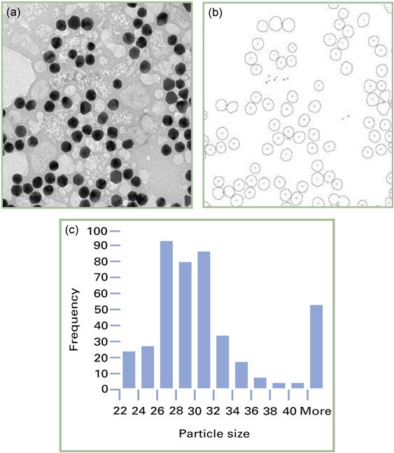
Traditionally, size measurements from electron microscope images are achieved by applying threshold intensity uniformly across the image. Image intensities above (or below) this level are taken to correspond to areas of the particle being measured. This is demonstrated in Figure 7.8(b), where a threshold was applied to identify the particles. Simple analysis allows the area and radius of the particle to be determined. In the case of non-spherical particles, the diameter is determined by the fitting of an ellipsoid. A histogram of the sizes can then be easily determined (Figure 7.8(c)).
Although the threshold method described above is a simple, well-defined and recognised method, it does suffer from some significant drawbacks. The first is setting the threshold level, which is difficult for poorly contrasting particles (such as small polymer particles or inhomogeneous particles) (Figure 7.9). The second, more important, drawback occurs when analysing agglomerated particles. With no significant intensity difference between the particles, a simple threshold is insufficient to distinguish between the particles and hence accurately determine size. It is usually recommended to use a watershed method.

The determination of the particle boundaries is the essential requirement for precise particle size measurement using electron microscopy. Because manual measurement is both tedious and a source of considerable non-reproducible errors, digital image processing is preferred whenever possible. Thresholding techniques are often used to separate objects from the background (see Ref. [66] for a review). Thresholding techniques rely, however, only on the distribution of grey scale values across the image, and the resulting size distribution is highly dependent on the chosen thresholding algorithm [67].
To reduce uncertainties, other information, such as the image acquisition parameters and details of the scattering process, can be used. For size measurements, threshold levels of the nanoparticles can be calculated using Monte Carlo simulations of the image formation process. The signal level of the transmitted electrons at the particle edge is then calculated by taking into account all relevant parameters of the instrument (e.g. electron energy, probe diameter, detector acceptance angle and energy sensitivity) and of the specimen (material, density, estimated particle size). Frase et al. [68] give an overview of programme packages used for SEM. Some of these packages are also able to model transmitted electrons and their detection.
Once the nanoparticles are separated from the background, a particle analysis routine [69] can be used to calculate the desired diameter; equivalent spherical, Feret or other. When image analysis is varied automatically, artefacts such as dried chemicals or touching particles are falsely included as identified objects. Depending on the size of the data set, their effect may be removed by hand or automatically via limits of some geometrical parameters, limits for the minimum and maximum size or circularity when analysing nearly spherical particles. It is recommended that such limits are set with great care and to verify that they do not alter the size distribution significantly. The use of watershed algorithms, which work by assuming that an image is a topographical surface and then modelling the flow of water upon this surface [70], often lead to systematic underestimation of the size. If high precision measurements are required, it is, therefore, advised that touching and overlapping particles should not be included in the measurement.
7.6.4.1 Sources of uncertainties
There are multiple sources of errors that contribute to the uncertainty associated with the determination of the mean particle size.
• Calibration of the pixel size: the uncertainty related to the calibration of the pixel size is due to imperfect reproducibility, drifting instrument conditions, etc. The uncertainty of the stated pitch values of the calibration artefact also has to be included.
• Digitisation: leads to errors because a round object is converted to a number of square pixels. By interpolating image regions of interest, the impact of digitisation may be decreased.
• Pixel noise: depending on the instrument performance and the image quality, image noise at the boundary of the particle may lead to erroneous inclusion or exclusion of pixels.
7.7 Other particle beam microscopy techniques
In order to get high-resolution images from any scanning beam microscope, one must be able to produce a sufficiently small probe, have a small interaction volume in the substrate and have an abundance of information-rich particles to create the image. A typical SEM meets all of these requirements, but other particles can be used as well. Recently, an FIB [71] has become more and more popular. The concept of FIB is similar to that of SEM; however, the electrons are replaced by ions of much larger masses. As a consequence they can in general induce damage to a specimen by sputtering. However, for each incoming ion, two to eight secondary electrons are generated. This abundance of secondary electrons allows for very high-contrast imaging. In addition to secondary electrons, backscattered ions are also available for imaging. These ions are not as abundant as secondary electrons, but do provide unique contrast mechanisms that allow quantitative discrimination between materials with sub-micrometre spatial resolution.
An electron beam has a relatively large excitation volume in the substrate. This limits the resolution of an SEM regardless of the probe size. A helium ion beam does not suffer from this effect, as the excitation volume is much smaller than that of the SEM. SEMs are typically run at or near their secondary electron unity crossover point to minimise charging of the sample. This implies that for each incoming electron, one secondary electron is made available for imaging. The situation with the helium ion beam is much more favourable.
The helium ion microscope [72] has several unique properties that, when combined, allow for higher resolution imaging than that available today with conventional SEMs. In addition to better resolution, the helium ion microscope and the FIB also provide unique contrast mechanisms in both secondary electron mode and backscattered modes that enable material discrimination and identification.