
Wearable Algorithms
An Overview of a Truly Multi-Disciplinary Problem
Guangwei Chen, Esther Rodriguez-Villegas and Alexander J. Casson, Imperial College, London, UK
This chapter introduces and comprehensively overviews emerging wearable algorithms for embedding in to wearable sensor nodes. We begin with an overview of some of the potential benefits of low power real-time signal processing in wearable sensors with a particular focus on increasing the operational lifetime. Measured results from a practical state-of-the-art sensor platform demonstrate and quantify the design trade-offs present and the potential system optimizations available. We then consider the theory behind wearable algorithms and highlight the key properties of power–lifetime trade-off, big data performance testing, and performance–power trade-off that differentiate these new algorithms from conventional signal processing approaches. We conclude by reviewing the state-of-the-art in low power algorithms implemented in hardware and highlight the key design techniques that are now emerging to realize the lowest possible levels of power consumption.
Keywords
Accurate performance testing; algorithm design; battery selection; circuit design; design trends; embedded signal processing; low power consumption; msp430; real-time signal processing; sensor node optimization; wearable devices
1 Introduction
Wearable sensors are quickly emerging as next-generation devices for the ubiquitous monitoring of the human body. Illustrated in Figure 1, these are highly miniaturized sensor nodes that connect to the body and record one (or potentially more) physiological parameters before wirelessly transmitting the recorded signals to a base station such as a smartphone, PC, or other computer installation.

For end users there are a number of features that successful wearable sensors must include: it is essential that they are easy-to-use, socially acceptable, and long lasting. The power consumption of the sensor node is a critical factor in realizing all of these features as the current draw of the sensor sets the physical size of the battery required, which determines the device size and operating lifetime, which in turn affects the ease of use.
To illustrate current trends, Table 1 shows the 2013 performance of ten state-of-the-art wearable units for monitoring the human EEG (electroencephalogram [1]). It can be seen that a number of high-quality, highly miniaturized units are now available commercially and that these can easily offer over 8 hours of recording time. Twenty-four hour recording periods are starting to be offered by research stage units. This level of power performance is likely sufficient for performing any one EEG recording experiment.
Table 1
Approximate specifications of 2013 state-of-the-art low channel count EEG systems for wearable brainwave monitoring. Many devices come in different models and configurations; only one potential configuration is reported here. Physical sizes are as given by the manufacturer and are not directly comparable: some are for the recorder unit alone while others are for the complete recorder plus electrodes system.
| Device | Actiwave [2] | Emotiv [3] | B-Alert [4] | Neurosky [5] | Sleep zeo [6,7] | Enobio [8] | Cognionics [9] | Quasar [10] | Mindo [11] | IMEC [12,13] |
| Channels | 4 | 14 | 4 | 1 | 1 | 8 | 16 | 12 | 4 | 8 |
| Sampling frequency [Hz] | 128 | 128 | 256 | 512 | 128 | 500 | 500 | 240 | 512 | 1000 |
| Resolution [bits] | 8 | 14 | 16 | 12 | 12 | 24 | 24 | 16 | 16 | 16 |
| Size [mm] | 37 × 27 × 8.5 | – | 127 × 57 × 25 | 225 × 115 × 165 | – | 225 × 115 × 165 | 46 × 56 × – | – | 165 × 145 × 50 | 165 × 145 × 50 |
| Weight [g] | 8.5 | 116 | 110 | 90 | 24 | 65 | 75 | 500 | 100 | 100 |
| Battery life [hours] | 13 | 12 | 8 | 8 | 8 (1 night) | 8 | 4 | 24 | 20 | 20 |
| Wireless? | No | Yes | Yes | Yes | Yes | Yes | Yes | Yes | Yes | Yes |
| Dry electrodes? | No | No | No | Yes | Yes | Yes | Yes | Yes | Yes | Yes |
| Status | Commercial | Research | ||||||||

However, the power level still falls far short of creating simple pick up and use devices. Substantial improvements in system power consumptions are required to realize units that can be reliably re-used session after session without having to worry that the device will stop working due to the battery. This is a major source of frustration for users, and limited battery life is the major obstacle to the widespread deployment of wearable sensor systems today. Strategies for maximizing the operational lifetime in next-generation devices are therefore essential.
This chapter will explore how low-power signal analysis algorithms can be integrated into wearable sensors in order to improve the operational lifetime. We will demonstrate that while there are many examples of low-power electronics available in the literature, and similarly many examples of automated processing algorithms, creating successful algorithms for use in a wearable device is not a matter of just connecting the two together. Instead, new wearable algorithms are emerging at the interface of these disciplines, and these rely on the close fusion of the application requirements, the sensor node design, the signal-processing design, and the electronic design in order to realize the lowest possible levels of power consumption and to maximize the battery lifetime.
Our objective is to provide practical insights into the creation of these new algorithms. In section 2 we consider the detailed power performance of a current sensor node based on Texas Instrument’s popular MSP430 processing chip [14]. This study allows us to demonstrate the design trade-offs present, and the benefits of on-sensor node signal processing in terms of both maximizing operational lifetime and in increasing the range of battery technologies that are suitable for use with a particular senor. Based on this, in section 3 we consider the theory behind wearable algorithms and establish the key objectives that successful algorithms and hardware implementations must meet. This allows us to explore current and emerging techniques for realizing wearable algorithms using very low-power consumption dedicated circuitry in Section 4. We conclude by summarizing the 2013 state-of-the-art and motivate future developments as we move towards realizing truly wearable algorithms for our wearable sensor nodes.
2 Why Do Wearable Sensors Need Algorithms?
We begin by investigating the practical challenges in the design of miniature wearable devices that use standard off-the-shelf components. Our goal is to minimize the device volume and maximize the device-operating lifetime, while under the constraint of having restricted hardware resources available. We will see how this motivates the use of online, real-time, signal processing as part of the device design and in turn, in section 3, how this leads to wearable algorithms.
The key to the success of a wearable device is the minimization of its size and weight as these directly affect the device’s discreteness and comfort. As surface mount components are nowadays small compared to batteries, leaving aside the application-specific interface/electrode(s), the size of the batteries dominates the overall volume of the sensor node. The essential starting point in node design is therefore a consideration of suitable battery technologies, sizes, and performances (section 2.1). We can then consider the hardware platform used to collect the physiological data (section 2.2) and the wireless transmitter used (section 2.3). The design decisions made at this stage have a large impact on the node operating lifetime, and the presence of any online signal processing, as we will see in a practical design example (section 2.4).
2.1 Battery Selection
To guide our investigation, Table 2 summarizes the specifications of four off-the-shelf primary batteries from three different size groups that are potentially suitable for powering wearable sensor nodes. This shows five battery specifications that are critical to consider for low-power wireless design. The physical size, which as discussed above dominates the device volume, and the energy storage capacity, typically expressed in mA-hours, are the well-known parameters. However, all batteries also have an internal resistance, and this means that the energy stored cannot be optimally discharged into all possible loads. This leads to further important battery parameters, which are discussed below.
Table 2
Specifications of four non-rechargeable disposable batteries potentially suitable for wearable sensor nodes with varying physical sizes and battery technologies. Three classes of battery size are considered: the cylindrical cell (CYC), button cell (BC), and coin cell (CC). (Rechargeable lithium polymer (LiPo) batteries can have higher energy densities than the chemistries listed here, but the minimum physical sizes available are also generally bigger.)
| ID | Group | Name | Type | Nominal Voltage [V] | Max Continuous Current [mA] | Nominal Current [mA] | Nominal Capacity [mAh] | Size (Diameter × Height) [mm × mm] |
| B1 | CYC | Xeno XL-050F (1/2 AA) [15] | LiSOCl2 | 3.5 | 50 | 1 | 1200 | 14.5 × 25.2 |
| B2 | BC | Duracell DA675 (Size 675) [16] | Zn(OH)4 | 1.4 | 16 | 2 | 600 | 11.6 × 5.4 |
| B3 | BC | Duracell DA13 (Size 13) [17] | Zn(OH)4 | 1.4 | 6 | 0.9 | 290 | 7.9 × 5.4 |
| B4 | CC | Renata CR2430 [18] | LiMnO2 | 3 | 4 | 0.5 | 285 | 24.5 × 3.0 |

2.1.1 Supplied Voltage
Firstly, the supplied battery voltage must meet the operation requirements of the electronic circuitry used in the wearable device. Importantly, the supplied voltage is not the same as the battery nominal voltage as there will be an internal voltage drop in the battery due to the internal resistance, and this drop will vary depending on the current draw. Most off-the-shelf low-power microcontrollers and transceivers today require somewhere between 1.8 V and 3.6 V, and batteries that supply a voltage outside this range must be used with a DC-to-DC voltage converter or stacked in series to increase the delivered voltage. However, these techniques reduce the battery lifetime due to either the extra power consumption from the additional circuitry or due to the increased internal impedance.
2.1.2 Maximum Continuous Current
Secondly, the maximum continuous current (also referred to as the maximum average current supply), Iavg(max), limits the average current draw from the battery. In theory, a 200 mAh battery can provide 1 mA for 200 hours, or 200 mA for 1 hour. In practice, each battery actually has a maximum supported current draw and if more current than this is drawn the effective capacity will not be the full 200 mAh reported value. The average current required by the system must be smaller than the corresponding Iavg(max) for the specific battery. Otherwise, more than one battery will have to be used in parallel, possibly together with diodes to prevent any non-rechargeable batteries from inadvertently charging. Again, the battery must be able to provide this current without a significant drop in its voltage supply because of the internal impedance.
2.1.3 Maximum Pulse Current Capability
Thirdly, for short periods a battery can provide more than Iavg(max), up to a maximum pulse value Ipulse(max). Ipulse(max) must be large enough to guarantee that variations in the supply voltage, which will drop if the current consumption increases, will not exceed the operating range of any circuit in the wearable sensor. The value of Ipulse(max) is a function of how long the pulse must be provided (the hold time); Figure 2 shows typical maximum values of pulse current with various pulse widths for the batteries listed in Table 2. There is a clear decrease in the maximum pulse current that can be provided as the duration of the required pulse increases. This is of particular importance when selecting the radio transceiver block and protocol as this generally determines both the peak current draw and how long it is required for.

2.1.4 Effective Capacity and Lifetime
Combining the above effects allows the effective battery capacity (Ceff) to be found. This is a critical parameter for long-term monitoring applications and it will generally be smaller than the nominal battery capacity, unless the system average current consumption (Isys) matches the manufacturer’s recommended value (also referred to as the nominal current or the standard discharge current). The value of Ceff is hence a function of Isys and it will be lower than its nominal value when Isys is larger than the nominal current.
Based on this, in order for a certain battery to be a viable option for a specific system it must meet the system requirements not only in terms of size and supply voltage, but also in terms of the average and maximum dynamic currents that the system needs to operate. Once the necessary conditions are met the lifetime of the battery, LT(Isys), can be determined as
(1)
Figure 2 also shows a plot of the measured battery lifetime LT(Isys) versus the average current consumption Isys for our battery examples. From this it is clear how, although the CYC battery used requires more volume, it also provides much better performance in all other aspects. Comparatively the zinc-air BC batteries have similar performance only if the effective average current drain is higher than 1 mA. This is due to their high self-discharge characteristic when exposed to air, and for applications with ultra-low effective power consumption (i.e., Isys<1mA) zinc-air batteries should be used with air management so that only a limited (but necessary) amount of air goes into the batteries. Alternatively, in cases when the continuous current is not a limiting factor, the CC battery may be preferable since it has a superior combined performance in terms of self-discharge rate and pulse current capability.
2.2 Hardware Platform
The hardware platform in a wearable sensor node is responsible for collecting the physiological data (data acquisition) and for packaging and passing this data to the wireless transmitter. It must also control the transmitter operation (wireless transmission control), and there are a number of design factors that need to be studied.
2.2.1 Data Acquisition
As shown in Figure 1, a general wearable sensor may contain signal conditioning circuitry (typically an amplifier and an analog-to-digital converter (ADC)), and some optional signal-processing blocks to reduce the amount of data for wireless transmission. In the signal-conditioning block there is at least one anti-aliasing filter that restricts the bandwidth of the input signal before passing it to the ADC. For wearable applications seeking to minimize size, the anti-aliasing filter may be realized as a first-order RC low-pass filter. This is a physically very small circuit, but its use will come at the cost of requiring a higher ADC sampling frequency to ensure that the analog input signal is correctly represented in the digital domain. In turn, this implies that the amount of data passed through the system is increased, leading to an increase in power consumption due to the data multiplication. If desired, and as considered in section 2.4, downsampling of the data can be performed in the digital domain to obtain data compression. It is to avoid similar data multiplication that successive approximation register (SAR) ADCs tend to be preferred in wearable applications, rather than Σ-Δ ones, which are intrinsically based upon oversampling. In addition, SAR converters can operate with a lower peak dynamic current.
2.2.2 Wireless Transmission Controller
After acquisition, the physiological data is temporarily stored in a buffer and packetized to be sent to the wireless transmitter. During this process the controller decides on the structure of the transmission protocol, including the total size of a packet frame (Lframe) and the size of the packet header. Both limit the amount of physiological data (Ldata) that can be carried in each over-the-air data packet and mean that the full over-the-air rate available to the wireless transmitter cannot be used to transmit useful physiological data. The utilization of the protocol (ηprotocol) for the data can be expressed as
(2)
where Rair is the over-the-air data rate and Tlatency is the total latency introduced by the data acquisition, packet packaging, and transceiver interfacing.
Note that although longer packet sizes increase the data throughput and relieve the communication overhead, they also increase the transmission time, exponentially increasing the risk of interruption from undesired radio frequency (RF) interferences. This error rate will be explored in more detail below. Further, to avoid extra transceiver control complexity and overhead, the length of each data packet should be designed to match the size of the buffer present in the transceiver being used. This prevents the buffer from overflowing, and here we consider using this optimal packet size only.
2.3 Wireless Transmitter
Finally, the packetized physiological data is passed to the wireless transmitter, which sends it out to the sensor node base station. There are three factors that dominate the power consumption at this stage: the quality of the packet transmission, the hardware overhead, and the over-the-air data rate.
2.3.1 Quality of the Packet Transmission
Unstable transmission quality can cause unnecessary retransmission overhead or even packet loss. The successful transmission rate (ηtx) for one packet can be calculated as
(3)
where PER is the packet error rate, BER is the bit error rate, N is the bit length of a packet, and φQOL, the quality of link (QOL) factor, which estimates the probability of the RF channel being clear throughout the transmission process. It decays with longer transmission times.
From (3) it can be seen how a long packet size is not advisable. Also, the QOL of radio transceivers is affected by the transmission range and the transmission power. Long transmission ranges decrease the strength of the RF signal and hence lower the QOL. Generally, the transmission RF power can be tuned to trade-off QOL and power consumption.
In addition to this, to compensate for the BER and improve the link quality, chip manufacturers have introduced different features into transceivers so as to strengthen their error tolerance capability. Forward error correction (FEC) and automatic acknowledgement (auto-ack) are two examples that will be used in the test cases considered below. However, the use of these can come with extra cost, the largest one being FEC, which sacrifices half of the available bandwidth to create redundancy.
2.3.2 Hardware Overhead
In order to allow the wireless transmitter and receiver to recognize each other, and to synchronize, the transceiver appends a preamble signal (with size Lpreample) and its own transmission identification data (with size Ltxid) to the front of every packet automatically. Once the packet reaches the receiver these extra bits are examined and removed by the packet-handling hardware. Again, this results in not all of the over-the-air data rate being available for useful data transmission. The hardware efficiency ηhw is a key factor in this and can be calculated as
(4)
where the last term in the denominator accounts for a certain overhead generated by the time required to calibrate the PLL module of the RF synthesizer before transmission: Tcal is necessary in battery powered systems in order to avoid the frequency drift caused by variations in the supply voltage, and Tswitch is the time taken by the transitions between different low-power states.
2.3.3 Air Data Rate vs. Effective Data Rate
Given all of these factors the effective data transmission rate can be calculated, and this must be sufficient for the wanted application. Moreover, for the same amount of data, the faster the data rate the lower the effective power consumption as the transmitter can be turned off for more of the time. However, the overheads discussed in previous sections decrease the effective data rate and must not be ignored in power management. The effective bandwidth (Reff) of the transmission process can be estimated as
(5)
2.4 Practical Example and the Impact of Data Compression
We now take the design constraints from sections 2.1, 2.2, and 2.3 and apply them to a real sensor platform to demonstrate how they impact the node design and performance. Further, we also demonstrate the practical impact of on-sensor node signal processing for improving the operating lifetime. Our architecture is shown in Figure 3, and is based upon the popular MSP430 microcontroller to be representative of many current sensor nodes.

2.4.1 Node Design
Our system has a single channel that starts at the high-pass filter, normally used to eliminate out-of-band low frequency components such as electrode drift. This is followed by an amplifier that conditions the normally very weak signals for the subsequent blocks, a low-pass anti-aliasing filter (first-order RC filter made using discrete surface mount components) and a 10-bit SAR ADC, which is part of the MSP430 chip (MSP430F2274).
Here, we investigate two variants on this basic system: one using a Texas Instruments CC2500 transceiver as the transmitter stage and one using a Nordic RF24L01+ transceiver. Both of these operate in the 2.4 GHz band and are connected to the MSP430 by the serial peripheral interface (SPI) with maximum 10 MHz and 8 MHz clocks, respectively. The CC2500 has an option to enable FEC, while the RF24L01+ provides hardware support for auto-ack.
We use Texas Instrument’s SimpliciTI protocol stack with both transceivers, although it was originally designed for the CC2500 only. SimpliciTI is a low-power, lightweight wireless network protocol dedicated for battery-operated devices that require long battery life. From [19] the header of a non-encrypted SimpliciTI packet frame contains 96 bits. Because the RF24L01+ has half the buffer size of the CC2500 (256 bits), one field in the header is used to store the byte length of the user data, and this has been modified for the RF24L01+. In the user data field we add a time stamp for the recording, 20 bits in length, to each packet as an additional header. Given the memory constraints of the used MSP430 the rest of the space in a packet allows the CC2500 to transmit 34 samples (340 bits), whereas the RF24L01+ can transmit 18 samples (180 bits). In total, the packet size is 456 bits for the CC2500 and 294 bits for the RF24L01+.
To maximize the data throughput, minimize latency, and allow the transmitters to be duty cycled to reduce the average power, the air data rates of the transceivers are set to their maximum values: 500 kbits/s for the CC2500 and 2 Mbits/s for the RF24L01+. As recommended in [20], the preamble signal of the CC2500 is set to 96 bits. The RF24L01+ has 8 bits fixed preamble length [21] and both the CC2500 and RF24L01+ have extra identification data appended by hardware with lengths of 16 and 19 bits. Overall, assuming 100% of QOL, the effective data rate can be calculated from Eqs. (2) to (5) as 106 kbits/s and 338 kbits/s, respectively.
2.4.2 Optional Data Compression
To cover the physiological range we assume a bandwidth of up to 1 kHz. However, due to the use of a first-order passive RC anti-aliasing filter we sample at 4 kHz. Given this oversampling we again investigate two variants on the system: one where we transmit all of the collected data and one where we first downsample the data by a factor of 2. This lets us explore the impact of even modest data compression on our node lifetime.
The downsampling is implemented using a tenth-order Kaiser window digital low-pass filter (FIR) running on the MSP430. Our MSP430 model contains no hardware multiplier to reduce the computational burden of this processing.
2.4.3 Power Performance Results
For the core system, excluding the wireless transmitter, Table 3 shows the current consumption of each block present. The typical current profiles of the two transceivers are illustrated in Figure 4, where label A marks the section corresponding to the transmission overhead, B marks the actual wireless transmission times, and C indicates the optional auto-ack reception.
Table 3
Measured current consumption of the hardware platform and its constituent parts, excluding the wireless transmitter. Note that the CC2500 system has a 10 MHz clock while the RF24L01+ uses an 8 MHz clock.
| Block | Peak Current [mA] | Duty Cycle | Effective Current [mA] |
| Sensor | 0.27 | 100% | 0.27 |
| Amplifier | 0.36 | 100% | 0.36 |
| 10-bit SAR ADC | 1.10 | 19.8% (45 μs per sample) | 0.22 |
| Compression by downsampling (optional) | 2.50 (CC2500 system) 2.10 (RF24L01+ system) | 57.5% (130 μs per sample) 71.9% (163 μs per sample) | 1.44 1.51 |
| Total | 4.23 (CC2500 system) 3.83 (RF24L01+ system) | – | 2.29 2.36 |


Combined with the wireless transmitter, the two systems are compared in Table 4, which shows the current consumption of the systems when tested over 24 hours using the different batteries given in Table 2. It can be seen how some configurations only pass the 24-hour test with certain batteries. Not all miniature batteries are suitable for long-term monitoring! This has direct implications on the kind (and number) of batteries that may be required in a specific design, and consequently on the device size. For 24-hour monitoring applications with 22 kbits/s data rate, the smallest wireless configuration can be achieved by using one lithium manganese dioxide CR2430 3V battery.
Table 4
Current consumption of the sensor nodes with compression enabled and disabled. Only some of the miniature batteries listed in Table 2 are capable of powering the system for 24 hours.
| Transmitter | Configuration | Effective Current [mA] | Peak Current [mA] | Batteries Passed |
| CC2500 | Compression off, FEC off | 15.8 | 24.3 | B1 |
| Compression off, FEC on | 18.5 | 24.3 | B1 | |
| Compression on, FEC off | 7.4 | 25.6 | B1, B2 | |
| Compression on, FEC on | 13.5 | 25.6 | B1, B2 | |
| RF24L01+ | Compression off, auto-ack off | 4.5 | 14.3 | B1, B2, B3 |
| Compression off, auto-ack on | 5.6 | 15.2 | B1, B2, B3 | |
| Compression on, auto-ack off | 3.5 | 15.1 | B1, B2, B3, B4 | |
| Compression on, auto-ack on | 3.8 | 16.1 | B1, B2, B3 |

Turning on the data compression leads to substantial reductions in the effective current drawn by the system. Reductions by 20 to 30% are achieved, and in the CC2500 case without FEC the reduction is 53%. In all of the cases this reduction allows more of the battery technologies from Table 2 to be used, giving greater freedom in the system design and in the optimization of the device size. In the best case the effective current consumption of the entire system goes down to 3.5 mA, equivalent to a net power consumption of 480 nJ/bit. It is important to highlight, however, that only reductions in the effective current are achieved by the data compression. There are no substantial differences in the peak currents, and in some cases these may now become the limiting factors in the system design.
2.5 Summary
Designing a wearable sensor node involves a careful set of trade-offs between the electronic components used, the battery technology selected, and the implementation of any real-time signal processing. This section has demonstrated that in battery selection, which dominates the end physical size of the device, both the average and peak current draws have to be taken into consideration. Our presented numbers can be used as a realistic guide for system designers when distributing their power budget and when estimating the size and kind of battery required to operate their device for a certain length of time. Further, quantitative measured results have shown for two different transmitters the potential benefits of onboard signal processing for increasing the operational lifetime of the device. The challenge now is to realize more advanced signal processing to extend the operating lifetime even further.
3 What are Wearable Algorithms?
Section 2 demonstrated that by simply downsampling data by a factor of two reductions in the total system, power consumption of up to 53% could be achieved. Moreover, this was done with the MSP430 active for up to 72% of the time. Clearly, if more data reduction could be provided, or if the signal-processing platform (our MSP430) could be turned off more of the time to reduce its effective power, even greater increases in operational lifetimes could be provided.
The challenge, of course, is in realizing accurate data reduction algorithms that can operate within the limited power budgets available. Wearable algorithms is the name given to the emerging signal-processing approaches attempting to do this, and they differ from conventional algorithmic approaches in three important respects. In this section we explore these in detail and establish the theory behind, and requirements of, wearable algorithms.
3.1 Power–Lifetime Trade-Off
The example given in section 2 showed one case where online data compression can be used to increase the operational lifetime of a sensor node and to allow more battery technologies and hence physical sizes. We now consider the more general case and put bounds on the performance required in order to provide power beneficial signal processing, following the analysis originally introduced in [1,22,23].
Considering the example system given in Figure 1, the power consumption of the entire system can be approximated by
(6)
where Psc is the power consumption of the front-end amplifier and any other signal conditioning such as the ADC and N is the number of simultaneous recording channels present with one front-end per channel. Palg is then the power budget available for implementing the signal-processing algorithm, while Pt is the power consumption of the transmitter. C is the ratio between the size of the raw physiological data and the size of the data actually sent from the transmitter. If the signal processing passes all of the collected data to the transmitter C=1, and as more data reduction is provided, this number decreases.
Transmitters are commonly specified in terms of the energy per bit (J) required to transmit data effectively, and in this case Pt can be approximated as
(7)
where fs is the sampling frequency and R is the resolution of the ADC, which together define the total number of bits of physiological data collected.
As a result, if the inequality
(8)
is satisfied, a system with data reduction will consume less power than one that doesn’t have data reduction present. Taking typical values [1,22], fs=200 Hz, R=12 bits, J=5 nJ/bit and N=8 channels, gives a maximum possible power budget (when C=0 so complete data reduction with no actual data transmitted) of 96 µW.
In reality C will be somewhat larger than zero, bringing this budget down. Also, to account for the approximations, and to ensure decent improvements in lifetime are provided for the effort expended, the typical power target may be reduced by a factor of 10 to approximately 1 to 10 µW. This is very low indeed, and occurs for a multi-channel wearable sensor node, as opposed to the single-channel system from section 2, as both more front-ends are required and there is substantially more physiological data to be transmitted.
As we established in section 2, minimum power consumption is not the only design criteria: more energy can potentially be provided if physically larger batteries are used, but at the cost of a physically larger device. For a battery of volume V and energy density D operating over a lifetime T, the system power budget available is
(9)
Combining (9) with (6) and (8) gives a three-way trade-off between the amount of data reduction achieved, the power budget available to implement the signal-processing algorithm, and the operational lifetime that is then possible. This trade-off is plotted in Figure 5, using the same values as before, and using Psc=25 µW. The normalized lifetime Tn
(10)
is plotted in place of T so that the curve is independent of battery technology.

This shows that if a 50% data reduction is provided by an embedded signal-processing algorithm within a 10 µW power budget, the operational lifetime of the eight-channel wearable sensor node can be increased by 15%. If 80% data reduction was achieved (C=0.2) the lifetime would be increased by 28%.
Inevitably these figures are approximations, and typical values need to be mapped to the wearable sensing situation under consideration, but in all cases the power budgets available are very low. In 2010 authors in the IEEE Signal Processing magazine posed the question: “What does ultra low power consumption mean?” and came to the conclusion that it is where the “power source lasts longer than the useful life of the product” [24]. This is exactly what is required for maximizing the operating lifetimes of our wearable sensors. However, to realize such low-power signal processing, huge advances in power performance are still required. The aim of wearable algorithms is to bridge this gap and to bring algorithm power consumptions down into the needed microWatt and sub-microWatt levels.
3.2 Big Data Performance Testing
Classic signal-processing algorithms are assessed in terms of the performance obtained and the cost of getting this performance. There are many different metrics that can be used to quantify these, but human physiological signals are highly variable and inevitably algorithms are not perfect leading to a trade-off between the performance and cost. For example, when attempting to detect events such as falls, a number of correct detections will be made along with a number of false detections. Different algorithms, and different versions of the same algorithm, can provide different trade-offs, and these can be plotted as a curve as shown in Figure 6.

Unfortunately, ensuring that this performance testing is accurate and representative of the actual underlying algorithm performance is a major challenge [25,26]. Here we illustrate one example situation to demonstrate this and show that it is very easy to inadvertently skew algorithm results so that they appear better or worse than they actually are.
In event detection algorithms there are three main metrics that are used to assess the operation. (Often the same metrics as discussed here are used, but under different names.) The sensitivity is the main performance metric and shows how many of the actual events that are present are correctly detected:
(11)
where TP is the number of correct detections (true positives) and FN is the number of real events that are missed and not detected (false negatives).
The specificity and the selectivity are then different cost metrics. The specificity shows how many non-events that should not be detected are indeed not detected:
(12)
where FP is the number of incorrect, false, detections of an event (false positives) and TN is the number of non-detections (true negatives). Often it is not easy to define what a true negative actually is. The selectivity shows what fraction of all of the detections made are in fact correct:
(13)
However, Eqs. (11) to (13) do not account for the fact that in the emerging Big Data era the available test data is made up of multiple different recordings, potentially from different test sites and with different durations and numbers of events present. To actually calculate a figure to plot on trade-off curves such as Figure 6 we need to take the results from each recording and combine the results together. This can be done in a number of ways.
Say there are M records available for testing, recorded from different people or from the same person at different points in time. Let each record be indexed by i. The arithmetic mean sensitivity can be found by calculating the sensitivity in each individual record and then averaging these values:
(14)
Alternatively, the number of correct detections and the number of missed detections can be summed separately to give the total sensitivity:
(15)
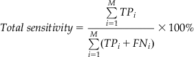 (15)
(15)
This treats all of the records as if they were one long record concatenated together.
The performance of an example EEG spike detection algorithm [25,26] using these two metrics is shown in Figure 7. It can be seen that these two approaches give quite different pictures of the performance, particularly in the 20 to 40% cost region. This occurs because one of the records available for testing contains many more actual events than the other records. Nevertheless, both reporting approaches are mathematically and conceptually correct, so which is more suitable for the performance evaluation?

This is just one possible example, and there are many other factors that can potentially skew reported performance results and that need to be taken into account (see, e.g., [27–29]). Of all of the challenges facing wearable algorithms, it is possible that performance metrics is the key one where there is still substantial need for exploration, improvement, and better understanding of how our algorithms actually operate over time and over multiple people. The availability of Big Data is driving this: it is no longer feasible or acceptable to test algorithms using data from just one subject, or to simply report the performance for each individual subject separately. Of course, in turn, wearable sensors are also driving Big Data: the aim of wearable sensors is prolonged physiological monitoring intrinsically giving us much more data to use in our algorithms.
3.3 Performance–Power Trade-Off
Finally, section 3.1 established that wearable algorithms need to operate with the lowest levels of power consumption, ideally into the sub-microWatt range. However, absent from the performance metrics discussion in section 3.2 was any consideration of the power consumption! True wearable algorithms are assessed in terms of the three-way trade-off between performance, cost, and power consumption.
Inevitably this leads to difficult decisions for the system designer: is it preferable to maximize performance, or to minimize cost, or to minimize power consumption? Is an algorithm with very low-power consumption, but comparatively low algorithm performance, a better choice than a higher power, higher performance algorithm? These choices are driven by the application that the wearable sensor is to be used in and there are many design options available. This leads to the key hallmark that differentiates wearable algorithms from previous approaches. Designs for wearable algorithms must span four levels: the human monitoring application design, the signal-processing design, the performance-testing design, and the circuit design, simultaneously. There are interactions between all of these different levels, making wearable algorithms a truly multi-disciplinary problem.
3.4 Summary
Wearable algorithms are a new discipline distinguished by the requirement for very low-power hardware implementations, Big Data performance testing, and power consumption aware performance testing. The algorithm design must also span four levels: the human monitoring application design, the signal-processing design, the performance testing design, and the circuit design, and exploit the new design trade-offs that are present when considering all of these levels at the same time. Inevitably this creates a very large design space to be explored, and this space is far from being fully mapped out. Nevertheless, there are emerging techniques that can be used to help realize wearable algorithms, and these form the subject of section 4.
4 Wearable Algorithms: State-of-the-Art and Emerging Techniques
The signal processing applied in the design example in section 2 was a relatively straight-forward downsampling of the physiological data, based on a tenth-order FIR digital filter. The MSP430 used did not have a hardware multiplier present and as such, while it was duty cycled to save power, the MSP430 was still on for up to 72% of the time. Even with this relatively modest duty cycling of the signal-processing platform, total power reductions of up to 53% were achieved. Using more sophisticated signal processing approaches, and coupling these with advanced hardware implementations, can offer even greater improvements in node lifetime. Potential avenues for achieving this are explored here to highlight the main developments.
4.1 Making the Signal Processing Algorithm
4.1.1 Procedure
Online signal processing for wearable sensors can take two forms:
• Application agnostic compression applied equally to all of the physiological data, essentially like making a zip file in real-time.
• Intelligent signal processing where analysis of the current data drives the operation of the senor node.
As we will see in section 4.3 most current wearable algorithms focus on this second option; the core stages required are shown in Figure 8. The raw input signal (y) is first passed to a feature extraction stage which emphasizes the points in the signal of interest: signal processing is applied such that interesting sections of the input signal are amplified relative to the non-interesting sections. For example, in ECG heart beat detection the aim would be to highlight the time at which the QRS complex occurs.

These features are then normalized to correct for the fact that physiological signals vary widely between different people and in the same person over time. This may be due to different underlying disorders present, changes in the signal due to age (as happens with the EEG [30]), or due to changes in the interface/electrodes(s) contact over time. Normalization aims to correct for these changes (to some extent) to allow reliable and robust operation of the algorithm, even if a subject-dependent classifier is used.
The final step is generating an output and using the input physiological signal to actually make a decision. Generally this takes the form of a classification engine that might provide a binary answer: Is a heartbeat present in this section of data? Is the subject awake or asleep? The output could also be multi-class: in this section of data is the subject awake, in light sleep (stages 1 and 2), deep sleep (stages 3 and 4), or in REM sleep? This output can then be used to control the operation of the wearable sensor node to maximize its operational lifetime. For example, in sleep monitoring applications the node might go into low-power mode whenever it detects that the human subject is awake. Alternatively, the sampling frequency of an ECG may be varied between a high rate during the heartbeat (QRS complex) and a low rate in between beats [31].
4.1.2 Feature Extraction
There are many possible features that could be chosen for use as the signal processing basis, and this forms one of the main design decisions impacting algorithm performance. Many of the algorithms considered in section 4.3 are based upon frequency domain information. For example, sleep onset in the EEG is known to be characterized by a reduction in the presence of 8 to 13 Hz (alpha) activity with this being replaced by 4 to 8 Hz (theta) activity [32]. The feature extraction in this case may therefore be a Fourier transform to follow the changes in these frequency bands. Alternatively, time-frequency transforms such as the continuous wavelet transform or discrete wavelet transform could be used [33,34].
For use in wearable sensor nodes the number of different features used is ideally minimized to reduce the power consumption and the number of circuit stages required. Hence it is important to make an optimal feature choice. A recent study that investigated 63 different features for highlighting seizure activity in the EEG [35] found that discrete wavelet transform-based features obtained the best performance (with an area under the performance curve of 83%), while fractal dimension and bounded variation features offered little over chance performance (53%). However, this doesn’t rule out the possibility that these other features if used with a different classification approach would get better performance, or that combinations of more than one feature could again lead to better performances.
Further, all features are also not equal in terms of the power required to calculate them, and this must weigh the choices made. Indeed when corrected for run time, [35] prefers a time-domain feature known as the line-length as the single best feature for highlighting seizure activity in scalp EEG.
4.1.3 Classification Engines
The simplest decision-making scheme is a threshold where the normalized input feature is simply compared to a fixed detection threshold:
(16)
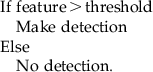 (16)
(16)This threshold can easily be varied to produce performance trade-off curves as shown in Figure 6 and has a very low computational complexity. Such an approach has been used in systems such as [35,36] to obtain low complexity performance.
More recently, machine-learning approaches have been used to automatically determine the best detection parameters, and this is particularly useful when dealing with multiple features and the need to select optimal separating planes between classes. Support vector machines (SVM) [37] are quickly becoming the most popular choice of machine learning approach as they achieve high classification accuracies and have recently been implemented at the circuit level with low-power consumptions [38–40].
4.2 The Hardware Platform: Analog Vs. Digital; Generic Vs. Custom
4.2.1 Analog Signal Processing
The physiological world that wearable sensors are attempting to monitor is intrinsically analog. Signals such as the EEG, ECG, or glucose concentration vary continuously and in continuous time. In contrast, the world of smartphones, PCs, and the Internet is digital with data represented by strings of binary data (either 0 or 1). These numbers can only represent finite, quantized input values and are taken at discrete time points at a particular sampling frequency. At some point a conversion between the two domains must take place, and this leads to a design choice over which domain to use when implementing wearable algorithms.
In 1990 Eric Vittoz published work on the fundamental power consumption limits of analog and digital processing, which has been since expanded on several times [41–43]. In the analog domain, the basic building block is taken as the integrator, modeled as an ideal transconductor charging and discharging a capacitor at frequency f. (A transconductor is an analog circuit block that outputs a current directly proportional to the input voltage.) The minimum power consumption required for this is found as [43]
(17)
where k is Boltzmann’s constant, T the temperature, and SNR the signal-to-noise ratio.
Similarly, in the digital domain the minimum required power consumption can be found by considering how many elementary operations are required, and the power consumption per elementary operation, Etr. For a single pole digital filter this is estimated as [43]
(18)
where B is the digital word length in bits. In general, Etr scales with the size of the CMOS technology used for the circuits, down to a fundamental noise governed limit.
These power equations are intended as fundamental limits and so based upon assumptions, in particular that the analog circuits are limited only by the noise floor. Several further bounds have also been derived since these, including ones that assume process variations and the matching of transistors further limits the analog circuits, and ones that offer more general modeling approaches [44,45]. Nevertheless, the underlying trends that (17) and (18) show are illustrative and widely accepted. They are visualized in Figure 9.

This shows that while the fundamental digital limit is well below the analog one, the practical limit can be a lot higher. Moreover, the analog limit is a strong function of the SNR ratio, and hence dynamic range, while for values over 6 bits the digital limit is a much weaker function. The result is that analog processing is generally accepted to be superior for low dynamic range applications. There are numerous sources that note the important role of analog processing systems in such applications, both presently and into the future (see, e.g., [24,45–47]). As a result, several of the signal-processing algorithms considered in section 4.3 incorporate some form of analog signal processing.
Beyond these general trends, however, determining the precise cross-over point for switching between analog and digital processing is very difficult for a particular circuit topology. In fact, even if this was known, the dynamic range of many physiological signals is highly debatable. The EEG systems considered in Table 1 used everywhere between 8 and 24 bits, while classical pen writer-based systems had a range of approximately 7 bits [48]. A key challenge is that once processing is started in the analog domain, additional ADCs to take the results into the digital domain want to be avoided, which means that all of the processing must be analog.
4.2.2 Fully Custom Hardware
The next choice is on the general design approach: to use generic off-the-shelf components that are easily available commercially or to fabricate custom-designed microchips that implement just the algorithm operations of interest and which can be highly optimized for the wanted application, or a mixture of the two. The general trade-off in performance is illustrated in Figure 10.

In general, the fully custom microchip is the preferred option as it allows complete customization, and so there are no possible excess blocks that are present but not 100% necessary. By implementing everything on the same silicon chip significant miniaturization can also be achieved compared to buying multiple chips and needing a larger PCB to connect everything together.
It is important to highlight that while this is the route to best performance it is inflexible, time consuming, and expensive. It is also not guaranteed to deliver the best performance, and careful design is required to minimize power consumption. For example, Figure 9 showed that the power consumption of digital processing is heavily dependent on the technology used to fabricate the microchip: the smaller the technology the lower the power consumption. However, for prototype runs and academic use the smallest processing nodes can be prohibitively expensive, potentially making off-the-shelf-devices that can use such nodes (due to having large fabrication runs) a better design choice.
This said, at present all of the algorithms investigated in section 4.3 use some form of custom microchip and there is little doubt that, while it presents significant design challenges, it is the best approach for realizing wearable algorithms today.
4.3 Towards Wearable Algorithms: Examples from the Literature
To investigate the state-of-the-art we systematically reviewed papers published in IEEE Transactions and other journals since 2010 that implement some form of algorithm for use in wearable sensors. The performances of these algorithms are summarized in Table 5 and discussed below. (Note that there are also algorithms for implantable sensors, e.g., [49,50], which are not considered here. Some of the designs reported here are for use in both implanted and body surface recordings.)
Table 5
Summary of current algorithms implemented in low-power hardware for wearable systems. Many papers report more than one operating point or setup and only one representative case is summarized here. (–) indicates that the information was not reported or was not clear for the case used. Unless trivial, to avoid extrapolations, performances are as given by the authors and have not been reprocessed to use consistent units, although this does make direct comparisons difficult. Note that some algorithms are single channel while others can analyze more than one channel of data at the same time.
| Paper | Aim | Features | Classifier | Algorithm Performance | Circuit Basis | Power Performance |
| GENERIC PROCESSORS | ||||||
| [51] | ECG heart beat detection | Frequency information (CWT) | Maxima detection and threshold | Sensitivity 99.65% Selectivity 99.79% | Custom CoolFlux processor | 12.8 pJ/cycle, 1 MHz clock, 0.4–1.2 V |
| GENERIC PROCESSORS WITH ACCELERATORS | ||||||
| [36] | EEG seizure detection | Frequency information (FFT) | Threshold | – | Custom ARM Cortex M3 processor | 0.99 μW, 0.8 V |
| [52] | EEG band power extraction | Frequency information (FIR filter) | – | – | Custom MSP430 core with FFT and CORDIC accelerators | 19.3 μJ/512 samples , 0.7 V |
| ECG heart beat detection | Frequency information (IIR filter) | Adaptive threshold | – | 16.4 μJ/heart beat, 0.7 V | ||
| [38] | EEG seizure detection | Frequency information (FIR filter) | SVM | – | Custom MSP430 core with SVM accelerator | 273 μJ/classification |
| 0.55–1.2 V | ||||||
| ECG arrhythmia detection | Time domain morphology | SVM | – | 124 μJ/classification | ||
| 0.55–1.2 V | ||||||
| [39] | ECG arrhythmia detection | Time domain morphology | SVM | – | Custom Tensilica processor with added instructions and SVM | 10.24 μJ/classification |
| 0.4 V | ||||||
| FULLY HARDWARE ELECTRONICS | ||||||
| [53] | EEG application agnostic compression | Compressive sensing | ~10 dB SNDR, x10 data compression | Custom digital circuits | 1.9 μW, 0.6 V | |
| [54] | ECG heart beat detection | Frequency information (DWT) | Maximum-likelihood type | Error rate 0.196% | Standard cell digital circuits | 13.6 μW, 3 V |
| [55] | ECG heart beat detection | Frequency information (DWT) | Maximum-likelihood type | – | Custom digital circuits | 0.88 pJ/sample, 20 kHz clock, 0.32 V |
| [40] | EEG seizure detection | Frequency information (FIR filter) | SVM | Detection rate 82.7% False rate 4.5% | Custom digital circuits | 2.03 μJ/classification 128 classifications/s |
| EEG blink detection | Detection rate 84.4% | |||||
| 1 V | ||||||
| [56] | ECG artifact removal | Time domain electrical impedance tomography | LMS adaptive filter | ~10 dB increase in Signal-to-Artifact power | Off-the-shelf MSP430 with analog co-processing | – |
| [31] | ECG adaptive sampling frequency | Frequency information (Band-pass filter) | R-peak search algorithm | x7 data compression | Off-the-shelf MSP430 with switched capacitor analog | 30 μW, 2 V |
| (Gives x4 power reduction of full system) | ||||||
| [57] | EEG band power extraction | Frequency information (Band-pass filter) | – | – | Switched capacitor analog processing | 3.12 μW, 1.2 V |
| [58] | EEG band power extraction | Frequency information (CWT) | – | – | Continuous time analog processing | 60 pW, 1 V |

Inevitably it is very difficult to capture all of the information and to directly compare different algorithms that are used for different purposes, with different algorithmic approaches, and assessed using different performance metrics, but Table 5 does provide key insights into the main approaches that are currently being used and the current state-of-the-art.
Broadly there are three categories of on-chip algorithm implementation present: firstly, highly optimized, but generic, on-chip processors that can be used to implement any algorithm using software; secondly, generic processors that are combined with application-specific features or accelerators to decrease the power consumption of the key signal processing stages; and finally, fully hardware-based algorithms.
4.3.1 Generic Processors
Our sensor node in section 2 was based on the MSP430 as an easy-to-use, easily available low-power platform. However, in active mode the power consumption was 5.5 mW (at 10 MHz clock, 2.2 V supply). Thus, to realize microWatt levels of power consumption this MSP430 must be powered down for very large amounts of time, limiting the signal processing that can be provided.
There have been a number of recent publications that implement platforms compatible with the MSP430 instruction set allowing algorithm code to be directly re-used, but with a reduced power consumption. The platform described in [59] presented such an architecture consuming 175 μW in active mode (at 25 MHz clock, 0.4 V supply). Note that this was partly achieved by the use of an advanced 65 nm CMOS technology, and for very low-power use the off/leakage current is substantial: 1.7 μW. No specific algorithm was presented for use on this processor and so it is not included in Table 5.
In contrast [51] presented a high-performance general processor based on the CoolFlux platform rather than the MSP430 instruction set. This was used to implement an ECG heart beat detection algorithm that consumed only 13 μW (single-channel analysis only). In active mode the processor core power consumption is 1.45 mW, with a high 100 MHz clock.
Analog signal processing is also possible on generic platforms, with [60] presenting a programmable analog chip operating from 2.4 V. This demonstrated an analog FIR filter that could be used for feature extractions and consumed 7 μW at 1 MHz, although again no full algorithm was presented.
4.3.2 Generic Processors with Accelerators
As seen in Figure 8, the main stages in a wearable algorithm are the feature extraction and classification. To improve power performance these stages can therefore be implemented in dedicated hardware while the rest of the algorithm is still implemented in software on a processing core. An algorithm for seizure detection based upon frequency band changes calculated using the FFT was presented in [36]. By providing dedicated hardware for calculating the FFT, while running the rest of the algorithm on a customized ARM Cortex M3 processor, this achieved an 18 times reduction in the power consumption with the total power being less than 1 μW. No measure of the algorithm detection performance was given, however.
Alternatively, [38] used a customized MSP430 core for calculating the features and then an SVM accelerator for reducing the energy impact of the classification stage. The rationale being that the features are often specific to an application, while the classification engine (the SVM) could be re-used in many different situations. This acceleration reduced the classification energy costs by up to 144 times compared to a software-only implementation, although for EEG processing the energy per classification is 273 μJ. Thus, if a fast update rate is required, the total power consumption may still be quite high. Similarly, [39] built upon this to also accelerate some of the feature generations.
4.3.3 Fully Hardware Electronics and Design Trends
Most of the works considered in Table 5 do not use any specific software platform and instead achieve very low-power consumption by using only dedicated and highly customized hardware circuits. While there are many different approaches to realizing low-power fully custom electronics, nevertheless a number of common design trends are seen.
Firstly, very low supply voltages (typically in the 0.5–1 V range, and down to 0.32 V in [55]) are widespread. This directly reduces the power consumption (as P=VI), but has a big impact on the operation speed of a circuit [55]. Physiological signals are normally low frequency, typically below 1 kHz, and so this trade-off is often acceptable provided that a large number of operations are not required. In addition, often multiple power zones are used with different supply voltages and clock speeds provided to different parts of a single chip depending on the processing required at a particular time. For example, [36] had 18 different voltage domains, while [52] had 15. Dynamic voltage scaling (allowing speed scaling), clock gating (where the clock is disconnected to prevent unnecessary switching), and power gating (where entire sections are turned off to reduce leakage currents) form different aspects of these multiple power zones.
Secondly, very few of the considered circuits are based purely on conventional architectures and a recurring theme is the use of new and simplified topologies. For example, [54] introduces a small modification to the classification process with a small impact on classification performance, but which more than halves the number of circuit blocks required to implement it. A new digital filter topology was introduced in [40], while [55] only used integer coefficients in the filter stages to simplify the multiplications required. The objective with these approaches is to minimize the system complexity and to minimize the transistor count. Doing this gives fewer transistors to power, fewer sources of leakage current, and hence power savings.
The third trend is for the use of analog signal processing, which is used in four of the algorithms considered and is a very powerful method for minimizing the transistor count. A hybrid approach was used in [31] and [56], whereby analog signal processing was combined with an off-the-shelf MSP430 for motion artifact removal and heartbeat detection, respectively. Both [57] and [58] use fully analog approaches for calculating frequency information.
All but three of the entries in Table 5 make use of frequency information as part of the signal-processing algorithm. It is by far the most common basis for the feature extraction stage, and as a result highlights the potential for the use of analog signal processing in this role. In particular, a recent publication [58] presented a continuous wavelet transform (CWT) circuit for performing time-frequency analysis on scalp EEG signals while consuming a nominal power of only 60 pW. This CWT is only a feature extraction stage, but the picoWatt power level is far below any of the other circuit blocks considered in this chapter. It is achieved by the use of very low processing currents and a fully analog signal processing approach. It highlights the potential key role of analog signal processing will have in future systems, and that there is real opportunity to create truly wearable algorithms where the power source lasts longer than the useful life of the product.
5 Conclusions
Wearable algorithms are an emerging truly multi-disciplinary problem where to achieve the lowest levels of power consumption innovations are required on multiple fronts: in the human-monitoring application design, in the signal-processing design, in the performance-testing design, and in the circuit design. This presents a large, four-dimensional, multi-disciplinary design space that has not yet been fully explored by a long way. Many challenges and opportunities are present, and while innovative design at all of the four levels in isolation will be beneficial, for future systems it is critical to exploit the multi-disciplinary factors present and the interactions between the different levels.
This chapter has presented a practical overview of the state-of-the-art in wearable algorithms with the aim of maximizing the operational lifetime of wearable sensor nodes: the detailed design decisions required in a typical system (section 2), the fundamental trade-offs faced by wearable algorithms (section 3), and the current low-power circuit techniques employed (section 4). Each one of these topics could easily occupy an entire book by themselves, but this would not allow the inter-disciplinary links to be drawn out, as we have attempted to do here and which we believe is essential for realizing truly wearable systems.
To conclude, we would reiterate that our aim here has been to maximize operational lifetime as this is the current major obstacle to the large-scale deployment of wearable sensors. However, wearable algorithms do not stop with increased battery life. We believe that there are at least eight essential benefits to using very low-power signal processing embedded in wearable sensor nodes:
• Reduced system power consumption
• Increased device functionality, such as alarm generation
• Reliable and robust operation in the presence of unreliable wireless links
• Reduction in the amount of data to be analyzed offline
• Enabling of closed-loop recording–stimulation devices
• Better quality recordings, e.g., with motion artifact removal
The challenge remains in realizing accurate algorithms that can operate within the power budgets available. As we have presented here, substantial progress has been made toward realizing these goals in recent years, and our examples should aid the designers of next-generation systems. Nevertheless, there is much progress still to be made in this rapidly evolving field, and much scope for substantially better intelligent systems in the future.