
Low-Power Integrated Circuit Design for Wearable Biopotential Sensing
Sohmyung Ha1, Chul Kim1, Yu M. Chi2 and Gert Cauwenberghs1, 1Department of Bioengineering at University of California, San Diego, La Jolla, CA, USA, 2Cognionics, Inc., San Diego, CA, USA
This chapter presents an overview of the fundamentals and state-of-the-art in non-invasive biopotential recording instrumentation with a focus on micropower-integrated circuit design for high-density and unobtrusive wearable applications. Fundamental limits in sampling, noise, and energy efficiency in the design of front-end biopotential amplifiers and acquisition circuits are reviewed, and practical circuits that approach these limits using metal-oxide-semiconductor (MOS) transistors operating in the subthreshold and weak-inversion regime are presented. The electrode-body interface is shown to be a performance limiting factor in practical non-invasive wearable systems, and examples are given of practical interface circuits and electrode systems for dry-contact and non-contact biopotential sensing obviating the need for gel or electrolytic ohmic contact to the body.
Keywords
Biopotential sensing; low-power technique; integrated circuit technique; biosignal acquisition; biomedical circuits; EEG; ECG; EMG; ambulatory monitoring
1 Introduction
Wearable sensor systems require long-term power autonomy with extremely limited power. Circuit techniques dictate the power consumption of the whole system. However, achieving the lowest possible power consumption must not sacrifice system performance. Systematic approaches with holistic considerations are necessary to realize intelligent low-power wearable sensors.
A solid understanding of the biopotential signals and the electrode-body interface is of primary importance for low-power, high-performance sensor design. Therefore, the first two sections review the basics of biopotentials and electrode-body interfaces.
The following considerations and requirements are essential to accomplish low-power circuits for wearable sensors:
• Low input-referred noise (1–5 μVrms)
• Low power consumption (<100 μW) optimizing noise energy efficiency (NEF)
• Application-dependent signal gain (1–1,000); variable gain in some applications
• Medium to high signal dynamic range (40–80 dB)
• Input impedance much higher than the electrode-body interface (>10 GΩ)
• Low to medium frequency range (0.1 Hz–10 kHz); configurable bandwidth in some applications
• DC blocking; or DC coupling not to be affected by electrode offset voltages
• High common-mode rejection ratio (CMRR>80 dB)
• High power supply rejection ratio (PSRR>80 dB)
• Rejection of mains interference
All these issues are inter-correlated in various ways. A deep understanding of the trade-offs and the challenges are required. The basic trade-offs and architectural design topologies are explained in the following sections. More specific design reviews for low-power amplifier and ADC are covered next. Lastly, more practical considerations for sensor designs are presented.
2 Biopotential Signals and Their Characteristics
Biopotentials, such as EEG, ECG, EMG, etc., are generated from volume conduction of currents made by collections of electrogenic cells. EEG is the electrical potential induced from collective activities of a large number of neurons in the brain. ECG results from action potentials of cardiac muscle cells, and EMG from contractions of skeletal muscle cells. Various other biopotentials (EOG, ERG, EGG, etc.) also result from collective effects of large numbers of electrogenic cells or ionic distribution.
Almost all biopotentials, including EEG, ECG, and EMG, of which characteristics are shown in Figure 1, range over very low frequency, typically less than 1 kHz. They are very low in amplitude, ranging tens to hundreds of μV when measured by a surface electrode. Since EEG and ECG range down to less than 1 Hz, recording of these signals faces challenges in electrode offset voltage, which may reach up to 100 mV, varying slowly over time. In addition, flicker noise of electronic circuitry, which is described further in Section 3.2, falls within the EEG signal range. Also, common-mode interference from the mains and irrelevant biopotentials should be sufficiently rejected.

3 Electrode-Body Interface and Electrode Noise
3.1 Electrode-Body Interface
The coupling of biopotential signals from the body into the front-end amplifier is accomplished through electrodes. At a fundamental level, the electrode interfaces ionic currents in the body with electrical currents in the electronic instrumentation. In practice, because the electrode comprises the first stage of the signal chain, its properties can dominate the overall noise and performance of the acquisition system, making its design and selection crucially important.
Broadly speaking, there exist three classes of biopotential electrodes in the literature: wet, dry, and non-contact (Figure 2) [3,4]. All types of electrodes ideally measure the exact same biopotential signals and are largely differentiated by the presence of a gel and the resulting contact impedance to the body.

Wet electrodes are the most common type and considered the ”gold standard” for both clinical and research applications. A typical wet electrode consists of a silver-silver chloride (Ag/AgCl) metal that is surrounded by a wet or solid hydrogel, containing chloride. Other kinds of metals can be used (gold is common for EEG) if the DC stability of the Ag/AgCl electrode is not necessary. The primary drawbacks with wet electrodes are its longevity and comfort. Wet electrodes degrade as the moisture content evaporates limiting its useful lifetime to, at most, a few days. Many users also report skin irritation and discomfort from the gels and adhesives that contact the skin.
Dry electrodes operate without the use of an explicit wet/gel coupling media. The metal in the electrode directly contacts the skin to couple biopotential signals. In practice, however, virtually all dry electrodes still rely on some degree of moisture which is gathered from the environment or emitted from the body (e.g., sweat). Compared to the wet electrodes, the performance of a dry electrode usually increases over time as more moisture permeates the skin-electrode interface, resulting in increased coupling. On bare skin, dry electrodes normally exhibit higher contact impedances than wet electrodes – on the order of hundreds of kΩ versus tens of kΩ [5]. However, with modern high input impedance amplifiers, this is rarely an issue. As with wet electrodes, Ag/AgCl contact materials tend to show the best performance, especially in terms of drift noise, which is important for diagnostic ECG applications.
There are also dry contact electrodes with capacitive coupling between the electrode and the body instead of coupling via galvanic conduction. Capacitive contact electrodes utilize a thin dielectric layer to form an insulated contact to the body. Compared to standard dry contact electrodes, capacitive electrodes offer a galvanically isolated, chemically inert surface, maximizing user safety and electrode longevity. However, the capacitive interface precludes the measurement of true DC potentials and may result in long settling times depending on the bias resistor and the amount of coupling to the body. In other respects, the capacitive contact electrodes operate similar to dry contact electrodes.
The final type of electrodes, non-contact, can be thought of as a special case of dry electrodes. They operate not only without gel, but also through an insulation layer such as clothing, enabling signal acquisition without direct skin contact. As expected, the coupling impedance can be very high, on the order of tens of pF in parallel with hundreds of MΩ. Obtaining acceptable signals requires the use of special, very high input impedance active electrodes. Because there is no direct skin contact, movement artifacts are a major, unsolved issue, especially for ambulatory use. Non-contact electrodes are also highly sensitive to environmental conditions such as humidity and the exact insulating material. Non-contact electrodes tend to work well on natural fabrics (e.g., cotton) under high humidity where the fabric actually becomes slightly conductive, offering a galvanic path to the skin. In contrast, it is difficult to obtain acceptable signals on high insulating synthetic fabrics (e.g., polyester) due to triboelectric artifacts.
3.2 Electrode Noise
In addition to the circuit noise from the amplifier components, electrodes can be a significant noise contributor in the signal chain [4,6]. Unlike circuit noise, however, comprehensive models for electrode noise do not exist, in part because the mechanisms for electrode noise are not well understood. In general, electrode noise is strongly correlated with the contact impedance, but the actual level is significantly higher than just the thermal noise from the resistive portion of the impedance.
The aggregate sum of the electrode noise sources can be quite large, on the order of μV/√Hz at 1 Hz, even for wet electrodes. This far exceeds the noise contribution of circuit components, illustrating the importance of proper electrode selection. Due to integrated current noise, both wet and dry electrodes have sharp 1/f2 spectra, which show up as baseline drifts in the time domain.
Non-contact electrodes can pick up additional noise from the insulating material between the metal and skin. As an example, acquiring signals through fabrics can be noisy due to the intrinsic high resistance of the fabric (>100 MΩ). This amounts to the equivalent of inserting a large resistor in series with the amplifier input and can add significant noise in the signal bandwidth.
4 Low-Power Analog Circuit Design Techniques for Biopotential Sensors
Power consumption of a circuit can be estimated by accumulating the products of supply voltage VDD for each block with its current. All strategies for low power design are simple combinations of reducing supply voltage and current. However, there are several considerations and limitations in pursuit of low power design without compromising the performance of the system. Trade-offs between noise, bandwidth, dynamic range, and several other should be considered, and a deep understanding of basic principles is necessary. Fundamental trade-offs and essential low-power analog design techniques for biopotential sensors are discussed in this section.
4.1 Subthreshold Weak Inversion Operation of MOS Transistors
Figure 3(a) illustrates a cross-section of fabricated NMOS and PMOS field-effect transistors in an integrated circuit CMOS process. Both have four terminals: gate (G), source (S), drain (D), and body (B). Their schematic drawing symbols are depicted in Figure 3(b). MOSFET operation can be separated into two modes according to the voltages between gate and source terminals: strong inversion and weak inversion (or subthreshold) operation, as shown in Figure 3 (c).

Counter to standard practices in analog CMOS circuit design, the weak inversion (subthreshold) region of CMOS operation has proven a favorable regime for low-power biomedical circuit design. In conventional design and particularly for high-speed applications, weak inversion operation has been considered as non-ideality in the cut-off region and its current has been labeled as leakage current. Recently, weak inversion has become increasingly important because its low power and low bandwidth characteristics are well suited for biomedical and other low-power sensor applications, owing to superior transconductance efficiency. Furthermore, transistors in deep submicron technology operating in weak inversion do not suffer from many process-dependent problems plaguing the above-threshold strong inversion region, such as gain-limiting effects of velocity saturation in electron and hole mobility [7].
Transistor model equations in weak inversion are simpler, are more transparent, and scale over a wider range than in strong inversion. The electron energy of a transistor in weak inversion is based entirely on the Boltzmann distribution, independent of process technology. The drain current through the transistor channel flows not by drift, but by diffusion, and changes exponentially with gate voltage. Thus, weak inversion operation is particularly well suited for implementing translinear circuits and log-domain filters.
Drain current IDS, transconductance gm, and unity-gain frequency ft in weak inversion are as follows [8]:
(1)
(2)
(3)
Because the transconductance is linearly proportional to drain current, so is unit-gain frequency. Thus, the trade-off between current and bandwidth is very straightforward: the larger the current, the wider the bandwidth.
Thermal noise in saturation and weak inversion is proportional to drain current as follows [9]:
(4)
where Δf is the signal bandwidth. The relative noise (inverse of the signal-to-noise ratio) is inversely proportional to drain current:
(5)
 (5)
(5)
Therefore, signal-to-noise ratio is linearly proportional to bias current IDS in weak inversion. For a majority of biomedical applications with narrow signal bandwidth, the lower currents of circuits in weak inversion still offer adequately large signal-to-noise ratio at maximum energy efficiency.
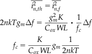
Flicker noise, also known as 1/f noise or pink noise, is also a significant noise source at low frequency. Random captures of carriers in traps near the Si/SiO2 interface and some other mechanisms are known to be a main source of 1/f noise [10,11], which is given by
(6)
where K is a process-dependent constant, W and L are width and length of the MOS transistor, and Cox is the gate oxide capacitance. PMOS transistors are known to have less 1/f noise than NMOS transistors, and therefore should be used in the input differential pair of a front-end amplifier for low-noise low-frequency applications in biosensing. Enlarging the MOS device size also decreases 1/f noise inversely proportional to area.
The 1/f noise corner frequency fc serves as an important indication for the proportion of 1/f noise relative to thermal noise over the spectrum. The 1/f noise corner fc is defined as the frequency at which 1/f noise and thermal noise are at equal magnitude, which in weak inversion is given by
(7)
 (7)
(7)
The 1/f noise corner can vary from a few 100 Hz to a few MHz depending on quality of process fabrication. Also, it depends on bias current: the lower the bias current, the lower the 1/f noise corner and hence the smaller the relative 1/f contribution to the overall noise.
For low-noise biomedical applications such as EEG acquisition, chopper stabilization techniques are widely used to reduce 1/f noise further. To be effective, the chopping frequency needs to be significantly higher than the 1/f noise corner frequency, typically ranging between 100 Hz and 10 kHz in these applications. Other techniques such as auto-zeroing and correlated double sampling can be used to reduce 1/f noise as well.
Three types of currents in MOS transistors need careful consideration in biomedical circuit design, below. These three are depicted in Figure 3(a) as subthreshold current Isub, gate leakage Ig, and pn-junction reverse-bias leakage Inp [12].
4.2 Requirements for Instrumentation Amplifiers
One of the most challenging parts in the design of wearable physiological monitoring systems is the implementation of instrumentation amplifiers (IAs), which acquire biopotentials from electrodes and perform analog signal processing and conditioning.
IAs are subject to almost all the challenging design specifications as discussed in the introductory section. As a point of reference, measured performances of some state-of-the-art IAs are shown in Table 1.
Table 1
Measured Performances of State-of-the-Art Instrumentation Amplifiers
| Harrison 2003 [13] | Yazicioglu 2008 [14] | Zou 2009 [15] | Verma 2010 [16] | |
| Application | Neural | EEG | Multimodal | EEG |
| VDD [V] | 5 | 3 | 1 | 1 |
| Power [μW] | 80 | 6.9 | 0.337 | 3.5 |
| Bandwidth [kHz] | 7.2 | N/A | 0.292 | N/A |
| Low-frequency Cut-off [Hz] | 0.025 | N/A | 0.005–3.6 | N/A |
| Input-Referred Noise [μVrms] | 1.6 | 0.59 | 2.5 | 1.3 |
| (0.025 Hz– 7.2 kHz) | (0.5–100 Hz) | (0.05–460 Hz) | (0.5–100 Hz) | |
| NEF | 4.0 | 4.3 | 3.26 | N/A |
| CMRR [dB] | ≥ 83 | > 120 | ≥ 71.2 | > 60 |
| PSRR [dB] | ≥ 85 | N/A | ≥ 84 | N/A |
| Input Impedance [MΩ] | N/A | > 1000 | N/A | >700 |
| (~ 20 pF) | (~ 8 pF) | |||
| Area [mm2] | 0.16 | 0.45 | < 0.5 | 0.3 |

4.3 Basic Instrumentation Amplifier
A classic three-opamp IA is adequate for achieving large input impedance, large CMRR, and sufficient gain. However, it consumes large power and area since it uses three amplifiers [17]. For a micropower biopotential acquisition front-end, the configurations shown in Figure 4(a) and (b) are widely used [13]. The AC-coupling input capacitors CC block electrode offset voltages. Owing to favorable matching performance of capacitors in integrated C.

In MOS processes, the gain can be precisely controlled. A large resistor Rf, typically substituted by a pseudoresistor or a switched-capacitor circuit (Figure 10), establishes DC biasing of the voltage at the input nodes of the amplifier and performs highpass filtering together with Cf. Mismatch in capacitor values results in degradation of CMRR. A practical CMRR that these architectures can achieve is about 60 to 70 dB. In addition, Cc dominates the input impedance. Therefore, the value of CC needs to be set by considering CMRR and the input impedance.
The transfer function of the IA is as follows [13]:
(8)
 (8)
(8)
where gm is transconductance of the OTA. Its passband gain is determined by the ratio of capacitors Cc to Cf. The high-pass cut-off frequency, fHP, is given by
(9)
The lowpass cut-off frequency, fLP, is controlled by the load capacitor CL and is approximately given by
(10)
when CL ![]() Cf and CC/Cf
Cf and CC/Cf ![]() 1. The right-half-plane zero at gm/2πCf can be canceled by inserting a 1/gm resistor in series with Cf. However, it can be ignored in many cases because it is located at much higher frequency than the frequency range of interest for biomedical applications.
1. The right-half-plane zero at gm/2πCf can be canceled by inserting a 1/gm resistor in series with Cf. However, it can be ignored in many cases because it is located at much higher frequency than the frequency range of interest for biomedical applications.
The main noise contributors of the single-stage IA are the OTA and the feedback resistor Rf. The input-referred noise due to these sources is
(11)
 (11)
(11)
where Cin refers to parasitic capacitance at the OTA input nodes VIN1 and VIN2 [17]. The noise from Rf can be dominant at low frequencies of interest. Thus, the following criteria needs to be met in order to reduce the contribution of the noise from Rf [18]:
(12)
In practical circuits, the noise from the OTA is typically dominant over the noise from Rf [18].
As a benchmark in the design of front-end IAs for low noise and low supply current, the noise efficiency factor (NEF) is used to compare the current-noise performance:
(13)
 (13)
(13)
where Vrms,in is the total input-referred noise, Itot is the total current drain in the system, Vt is the thermal voltage, and BW is the -3-dB bandwidth of the system [19]. NEF corresponds to the normalized supply current relative to that of a single BJT with ideal current load for the same noise level, defining the theoretical limit (NEF=1). In practice, differential IAs with input differential pairs incur twice the supply current for the same transconductance, with NEF values greater than 2. The state-of-the-art IAs typically have NEF of 2.5 to 10. It should be noted that NEF is a trade-off between bandwidth, noise, and current – not power.
4.4 Amplifier Design Techniques and Considerations
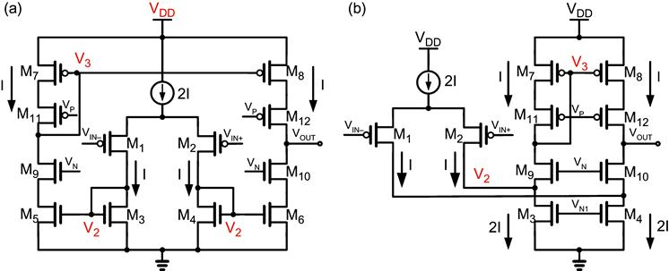
The operational transconductance amplifier (OTA) is the most important block in an IA, as shown centrally in Figure 4 (a) (single-ended) and (b) (fully differential). Among many kinds of amplifiers, the most popular two amplifiers, symmetrical OTA (or current mirror OTA) and folded cascode OTA, are shown in Figure 5 [13,16]. Both are one-stage amplifiers since both have only one high-impedance node at VOUT. The gain of both amplifiers is the product of the transconductance of the input pair and the output impedance. Fully differential amplifiers (not shown) add complexity in the design with the need for common-mode feedback, but offer superior CMRR and PSRR over single-ended solutions.
4.4.1 Noise and Power Perspective
Noise of the front-end amplifier for biomedical applications is critical. With given transconductances gm1 for M1-M2, gm3 for M3-M6 and gm7 for M7-M8, the input-referred thermal noise for the each amplifier in Figure 5 is as follows [13]:
(14)
(15)
where n is dependent on the capacitance ratio between depletion and oxide capacitance, which is generally between 1.2 and 1.8. In these equations, M1 and M2 are assumed in the weak inversion region while the others are in the strong inversion region. The effect from cascode MOSFETs are negligible in terms of noise. These equations clearly show that in order to obtain good noise performance, gm1 should be as large as possible. With a given bias current, the input pair transistors M1-M2 should operate in the weak inversion for higher gm/ID efficiency. In contrast, M3-M8 need to be in the strong inversion region in order to get lower gm. Due to the approximation that gm1 is much larger than gm3 and gm7, the input-referred noise is simplified by
(16)
With a proper sizing in the amplifier, there is only one factor that can be manipulated by circuit designers: current. Therefore, the trade-off between power consumption and noise is straightforward: the larger the current, the lower the noise.
For more stringent constraint in power consumption, the telescopic amplifier is superior to the other amplifiers because it has only two branches. However, output swing range is much narrower than the two amplifiers aforementioned.
The gm/ID Design Methodology
The gm/ID design methodology is very practical for low-power and low-noise design [20,21]. The transconductance efficiency gm/ID indicates the efficiency of a transistor in achieving higher gain with lower current. gm/ID is larger in the weak inversion than in the strong inversion, as shown in Figure 6(a). It means that a transistor operates more efficiently in weak inversion. As Figure 6(b) depicts, the operation region of a transistor with a given bias current can be manipulated by sizing for desired transconductance efficiency. However, it should be noted that larger device size for higher transconductance efficiency consumes larger area, inducing larger parasitic capacitances.

4.4.2 Stability Perspective
Negative feedback is utilized in almost all amplifiers to acquire a precise gain, set independent of the open-loop gain by a feedback ratio of linear passive components, along with widened bandwidth and increased noise suppression. However, feedback in high-gain systems may be subject to possible sources of instability, which requires careful design consideration. IAs for biomedical applications do not require wide bandwidth since the frequency range of interest is rather low, typically less than 1 kHz. However, due to low-power constraints, typical currents are a few tens to hundreds of nA, and transistors are typically sized large for better matching and low noise performance, resulting in low conductances over large parasitic capacitances, which may worsen the stability.
Figure 7 shows an open-loop Bode plot for the amplifiers. Since VOUT is the only high-impedance node (as mentioned above), the pole at VOUT is located at very low frequency. The feedback establishes the closed loop gain indicated by the dashed horizontal line in Figure 7. The intersection of the closed loop gain of the feedback and open loop gain of the amplifier determines the unity loop-gain frequency fK. The phase margin is given by
(17)
where fP2 is the second pole frequency. The position of the second pole is hence critical in the phase margin. If M3-M8 in Figure 5 (a) and (b) are assumed to have identical overdrive voltage, V3 node has larger gate capacitance due to the larger device size, and may generate the second pole. However, this pole is always followed by a zero due to double signal paths, so it does not affect the phase margin seriously. Furthermore, in a fully differential amplifier, the pole-zero pair at the V3 node is not induced. The pole at V2 may be lower than the pole-zero pair due to the large junction capacitances of M1 and M2, which are sized for large input-pair transconductance and low 1/f noise. In some cases, this may generate a doublet, causing relatively long settling time, although within acceptable range for biomedical applications.

4.5 Noise Across Sampling Capacitor
Thermal noise in a resistor can be modeled by the Nyquist-Johnson noise [22,23] as a series voltage source or a parallel current source as follows:
(18)
 (18)
(18)
Thermal noise, which is induced by random electron motions, is proportional to the absolute temperature.
An ideal capacitor induces no noise. However, due to ohmic coupling with nearby resistive elements such as switches in most practical settings, the integrated noise in a sampling capacitor is typically
(19)
It depends only on the capacitor size, other than absolute temperature. This also implies that the noise voltage is inversely proportional to root of capacitance. A 100-fold larger capacitor is required in order to decrease noise voltage 10-fold. Where kT/C noise limits the system’s performance, it is difficult to overcome noise just by enlarging the capacitor size.
Figure 8(a) depicts the main functional components of a typical biopotential sensor architecture. It consists of an amplification stage and an ADC with a sample-and-hold input. Figure 8(b) shows the input-referred noise due to the kT/C noise of the sample-and-hold circuit with respect to the capacitor size and the gain AV. The horizontal dashed lines refer to the required noise levels for sensing different types of biopotential signals. In order to avoid off-chip components, capacitor size is limited to be a few pF typically. Therefore, for the ADC with a sample-and-hold input, pre-amplification is required in order not to be affected by kT/C noise. Note though that for ADCs without sample-and-hold input such as a continuous ΔΣ ADC, pre-amplification may not be necessary.
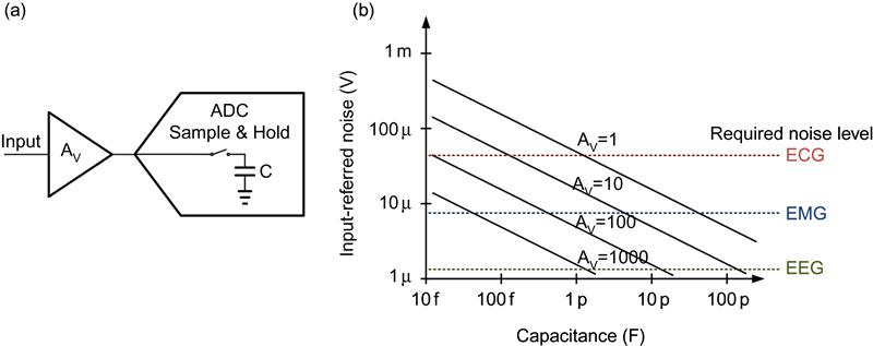
Autozeroing techniques to an AC-coupled front-end could in principle be used to bypass electrode offset voltage issues and cancel 1/f noise [24]. However, just kT/C noise for 1–10 pF sampling capacitance is about tens of μV as shown by the AV=1 curve in Figure 8 (b). Therefore other circuit techniques that do not rely on capacitive sampling, such as chopper stabilization, are typically used to mitigate low-frequency noise.
4.6 Chopper Stabilization Techniques
The chopper modulation technique is widespread and essential to mitigate 1/f noise and other low-frequency noise, such as popcorn noise, voltage offsets, and drifts. It is particularly used for sensitive acquisition of relatively weak biopotentials such as EEG, which requires very low input-referred noise, less than 1-2 μVrms.
The principles of the chopper modulation technique for amplifiers, which have been extensively studied [24–27], are illustrated in Figure 9. The low-frequency band-limited input signal Vin is modulated in front of the amplifier by a square-wave chopping signal. The resulting waveform is Va: now the signal is lifted to the chopping frequency fch, and the low-frequency aggressors do not fall within the signal band. After amplification and demodulation with the same chopping signal in Vb, the amplified input signal is shifted back to DC and the aggressors are now moved to fch. All the undesired aggressors and the harmonics are filtered out through the low-pass filter, and the desired input signal is restored at the output Vout.

There are mainly two challenges involved in the design of a chopper-stabilized amplifier: residual offset and output ripple [28].
The residual offset is mainly caused by non-idealities of the input chopper modulator. The mismatch of the clock-feedthrough and the charge injection in the input chopper generates spikes, which are demodulated at the output chopper into a residual output offset. In order to minimize the offset, at first, careful design and layout is required. A continuous [14,16,28,29] or digital [30] DC servo-loop can reduce the residual offset, and mitigate the signal distortion problem that is caused by the finite bandwidth of the amplifier. Also, filtering techniques [31–33] can be applied to resolve the issue.
Output ripple is induced by the input offset of the amplifier, and can saturate the output of the amplifier because the offset is also amplified. The ripple can be reduced by a continuous ripple-reduction loop [28] and a digital foreground calibration [30].
4.7 Pseudoresistors for Sub-Hz High-Pass Cut-Off
The high-pass cut-off frequency needs to be well below 1 Hz for typical biomedical signals, including ECG and EEG. The high-pass cut-off frequency of the typical IA in Figure 4 is determined by the time constant formed by its coupling capacitance Cc and feedback resistance Rf. Realizing sub-Hz time constants with on-chip capacitors and poly-resistors consumes an impractically large area for practical implementation in a chip. Using a 1–10 pF capacitor and a PMOS-based (MOS-bipolar) pseudoresistor is the dominant method. An alternative approach to implement high resistances is based on switched-capacitor logic.
The most prevalent solutions are PMOS-based MOS-bipolar pseudoresistors as shown in Figure 10(a–f). The most basic topology among these is a PMOS whose gate and body terminals are connected as in Figure 10(a) [34,13]. The gate-connected drain is recommended to be placed in a leakage-sensitive side such as the floating inputs of an OTA. The resistance between the two nodes VA and VB is at its maximum when they are equal. When VA>VB, the forward pn-junction current flows. When VA<VB, the through current is dominated by substrate leakage current. The two currents are unbalanced, and so is the resistance. The pseudoresistors of two PMOSs with different configurations are shown in Figure 10(b–d) [35,36]. A configuration with the PMOS gate connected to a bias voltage in Figure 10(e) results in a controllable resistance by gate voltage [36–38].

However, the resistance of the PMOS-based pseudoresistors in Figure 10(a–e) drops drastically when the voltage across moves away from zero, inducing signal-dependent distortion while limiting the voltage dynamic range [39]. The pseudoresistor in Figure 10 (f) has balanced resistance with wider linear range up to a few hundred mV. An even wider linear range can be achieved by using an auxiliary amplifier [40].
Switched-capacitors can be also used to implement high resistance on-chip as shown in Figure 10(g). In this topology, switching frequency fs controls the resistance precisely by
where C is capacitance of the capacitor in the middle. In order to obtain resistance as large as 1 TΩ, both fs and C should be made as small as C=1 fF and fS=1 kHz. However, a 1 fF is too small for manufacturability, and a 1-kHz clock is also not adequate for biomedical applications because of its close proximity to signal frequencies of interest. The switched-capacitor pseudoresistor in Figure 10(h) realizes a 10-fold resistance increase by charge sharing in the switched-capacitor circuits [16]. This topology mitigates the manufacturability and interference issues.
4.8 CMRR Enhancement Techniques
Common-mode interference is a difficult challenge for biomedical signal sensing systems. The major source of the interference comes from electric power lines, which are electrically coupled to the human body. High CMRR is required in the system to reject the common-mode interference in order to ensure high signal quality.
Accurate component matching between differential signal lines and between the channels is the most fundamental requirement to accomplish high CMRR. Good matching involves techniques from careful layout to smart architectural design choices. For example, the regulated cascode current mirror [41] in the current sources and the fixed-VDS input pair can enhance CMRR because the techniques decrease mismatch between the differential signals over wide dynamic range [33]. Furthermore, the mains interference can be rejected by a mixed-signal notch filter [42].
The most effective and popular techniques to enhance CMRR are active grounding by the driven right leg (DRL) technique and input impedance-boosting techniques.
4.8.1 DRL Technique
The DRL technique feeds the amplified input common-mode voltage into the body through an additional electrode, which has been placed on the right leg for ECG measurements. This negative feedback reduces the impedance in the feedback loop, attenuating the common-mode interference voltage at the sensor inputs [43,44] by factor of the feedback loop gain.
Figure 11 depicts an example implementation of a capacitive DRL circuit interfacing with a 3-OTA IA, requiring one additional OTA. VCM represents the common-mode voltage sensed as the average of the two electrode inputs. The DRL circuit drives this common-mode voltage to a virtual ground through high-gain feedback to the body. Ro is typically on the order of MΩ in order to limit current flowing to the body for safety.

From two electrode inputs, VIN+ and VIN-, to the DRL electrode VDRL, the gain of the negative feedback loop AV,DRL can be simplified by
20)
By the feedback, the electrode impedance and the common-mode voltage are reduced by factor 1+AV. In order to obtain large gain in the DRL circuit, an open-loop amplifier can be employed [45]. However, the feedback by the DRL circuit requires careful design for stability. Typically, large capacitance up to a few nF for Cf [46] is required to ensure stability due to variation in electrode impedances. A digitally assisted DRL circuit has the capability to have larger gain at the mains frequency for higher rejection and lower gain elsewhere for stability [47]. In dry electrode applications, common-mode feedback to one of the differential inputs in the front-end increases CMRR, and ensures its stability independent of electrode impedance variations [30].
4.8.2 Input Impedance-Boosting Techniques
Variations and mismatch in electrode impedances also degrade CMRR, reduce signal amplitude, and make the system more susceptible to movement artifacts. Thus, the input impedance of the biopotential sensor should be much higher than the impedance of the electrode and the interface between the body and the electrode. In many cases, the input impedance of biopotential sensors is limited by the parasitic switched-capacitor resistance of the input chopper [14,29,33] or by the AC-coupled input capacitors [13,15,16]. A positive feedback can bootstrap the AC-coupled input capacitors to boost the input impedance [30,48,49], achieving input impedance on the order of GΩ. In order to further boost the input impedance to TΩ levels, a unity-gain amplifier with active shielding can be used to bootstrap capacitance of the input transistor and all other parasitic capacitance [50].
5 Low-Power Design for ADCs
Digitization of recorded and processed analog signals is necessary for further digital signal processing and digital RF communication. The tight power and low noise constraints demand ultra-low power ADCs at low frequency range (1–10 kHz) without sacrificing noise performance, while requiring no or very little static current drain and scalable power consumption with respect to sampling rate for multi-modal recording applications. Both successive-approximation-register (SAR) ADC and oversampling ΔΣ ADC are superior architectures for achieving the specifications with the lowest power dissipation.
SAR ADC is the dominant architecture for low-power medium-resolution (8–10 bits) biomedical applications due to its simple architecture involving few analog circuits and its low power consumption at low frequency without static power consumption [16–17,45,51–56]. A typical SAR ADC consists of SAR logic, a clocked-comparator, and a capacitor input DAC as shown in Figure 12. It performs a binary-search-based successive approximation of the sampled input by controlling the switching logics of the input capacitor DAC while producing a one-bit quantization result per each clock from MSB to LSB [57–58].

There are many techniques and architectures to minimize the power consumption of an SAR ADC. Using main and sub binary weighted DAC arrays with a series attenuation capacitor can reduce the total size of the capacitor array; leading to reduced power consumption in the ADC driver and also in the capacitor DAC [59]. Also, the folded capacitor DAC architecture with divided reference voltages reduces the size of capacitor DAC, resulting in further power savings [52]. Using charge-recycling switching methods results in further saving of switching power consumption in the capacitor DAC [60].
SAR ADCs are generally considered to be most energy efficient for medium-precision low-sampling-rate digitization. However, most micropower SAR ADCs operate at signal levels substantially (3–4 orders of magnitude) greater than the typical signal level of physiological signals (Figure 1). They require a significant amplification before analog-to-digital conversion for sub-μV resolution. Furthermore, sampling at Nyquist frequency demands anti-aliasing filtering. The cost of amplification and anti-aliasing filtering are often not accounted for in ADC energy metrics. Most critically, sampling of biopotentials at μV resolution is problematic due to kT/C sampling noise on capacitors; several tens of μV for pF-range size limits on capacitors in integrated circuits.
ΔΣ ADCs are an alternative solution with the following strengths [61–65]:
• Resolution and sampling rate can be dynamically reconfigured, with sampling rate proportional to power consumption, so they are adequate for multimodal biopotential sensor applications.
• They include only a few simple analog components.
• They are suited for low-power and low-voltage operation.
• They can achieve high resolution such as 12–16 bits easily without complex circuit and layout techniques.
• For continuous-time ΔΣ topologies, there is no kT/C sampling noise.
A Gm-C incremental ΔΣ ADC with widely configurable resolution and sampling rate is shown in Figure 13 [61]. A transconductance (Gm) cell converts the differential input voltage signal to a current, approximately linear over the voltage range of typical biopotentials. The difference between this current and a feedback current is integrated and the resulting voltage is compared for three-level quantization of the feedback current, implementing a continuous-time first-order ΔΣ modulator. A continuous-time oversampling ADC avoids the need for anti-aliasing filter and sample-and-hold circuits preceding the ADC. In addition, its duty cycle control feature in the feedback offers precise digital gain programmability from 1 to 4,096.

Another example incremental ΔΣ ADC for non-invasive biopotential recording is given in Figure 14 [62]. It receives unbuffered biopotential signals and performs amplification, signal conditioning, and digitization using only a single OTA.

Another alternative solution for achieving high resolution for low-power biomedical applications is the hybrid architecture of SAR and ΔΣ conversions, as shown in Figure 15 [63]. It performs a successive approximation conversion in the first phase and ΔΣ conversion in the next phase with the residue from the previous phase. Thus, it can achieve more resolution than conventional SAR ADCs, and much shorter conversion time than typical ΔΣ ADCs.

In addition, there are other alternative ADC architectures such as an asynchronous level-crossing ADC [66] and a bio-inspired ADC with successive integrate-and-fire operation [67].
6 Low-Power Digital Circuit Design Techniques
Integration of digital circuits enables versatile programmable functionality in wireless sensor applications. Digital post-processing reduces the amount of data significantly, relaxing the power consumption in data communications. For example, digital pattern recognition embedded in wearable sensors is capable of detecting epileptic seizures without communicating all the data over a wireless link, leading to much power savings for the overall system [18,68]. In addition, various digital feedback and control signals may offer more adaptive functionality and better performance to the sensor operation.
Power dissipation in digital circuits is related to four factors – activity factor α relating the probability of a switching event, capacitance of the circuit C, clock frequency fCLK, and power supply voltage VDD:
(21)
The strategies to reduce power dissipation in digital circuits are simple: minimize each of the four factors.
6.1 Minimum Energy Design Methodology
Lowering power supply voltage VDD reduces the current drain in digital circuits drastically, and slows down the operation speed. To execute a given operation, operation of the digital circuit with lower VDD normally consumes less active energy, but drains larger leakage current due to longer operation time. Therefore, an optimized VDD, which is called the minimum energy point (MEP), exists where the power consumption for an operation is minimized considering both the active and leakage energy consumption [69–70]. The active energy consumption is as follows:
(22)
where Ceff is the average effective switched capacitance per the given operation. The leakage energy per the operation is given by
(23)
where β is a constant, and LDP is the logic depth of the critical path. The total energy consumption is the summation of the two energy components:
(24)
Figure 16 illustrates the location of the MEP as a balance between the active and leakage energies where the total energy is at the minimum. The MEP can vary by temperature and workload.

Several other techniques have been developed for optimizing the balance between high-performance and low-power digital circuits. We briefly outline a few of the prevailing techniques under continued development, each targeting one or more of the factors determining the power-performance trade-off:
• VDD: dynamic voltage scaling, voltage domain design, etc.
• Activity factor α: disabling of unused logics, clock gating, etc.
• Capacitance C: advances in CMOS technology, gate sizing, floorplanning for reducing wire lengths, etc.
• Clock frequency fCLK: dynamic frequency scaling, etc.
• Architectural methodologies: parallel processing, pipelining, retiming, unfolding/folding, etc.
• Leakage power: exploiting diversity in multiple threshold voltage devices, power gating, etc.
The details of these and other low-power digital circuit and architectural techniques are beyond the scope of this chapter and can be found in other books and papers, e.g., [68, 71–75].
7 Architectural Design for Low-Power Biopotential Acquisition
System-level architectural design may lead to significant advances in minimizing power consumption without compromising performance. Block-level design approaches should be considered before optimization within each block. This section reviews architectural design choices for low-power biopotential acquisition with some examples.
7.1 Architectural Design Strategies
An intelligent choice for functional block allocation in a system can result in significant improvements in power consumption and performance of the whole system. A typical architecture of wearable biopotential sensors comprises an analog front-end, a digital signal processor, an ADC between the two, an RF transmitter, and a power harvesting and management unit as shown in Figure 17.

Preprocessing inside of the sensor is more favorable than transmitting all raw data out, particularly in high-dimensional or high-bandwidth sensor applications where the amount of useful information may be significantly lower than the data rate requirements of the raw signals. Transmitting the processed data instead of all raw data reduces power consumption in the RF transmitter considerably. In the aforementioned example of seizure detection in EEG sensing, 18 electrodes produce 200-Hz 12-bit data resulting in a total data rate of 43.2 kbps. Employing digital processing for feature extraction and seizure detection reduces the data bandwidth to 2 kbps with a 10-fold reduction in power dissipation [18,68].
Equally importantly, energy-efficient analog preprocessing can lead to significant reduction of data bandwidth and power in the ADC and the digital block. A low-power ADC and digital blocks can substitute a high-performance ADC and digital signal processor. For example, typical EEG/ECoG-based brain-computer interface applications do not need raw data, but spectral characteristics of the recordings. Thus, extracting spectral power of the required frequency bands in analog front-end can reduce power dissipation and complexity in the other blocks [76]. There are many other kinds of analog preprocessing for low-power high-performance biosignal processing such as the QRS detection in ECG [77].
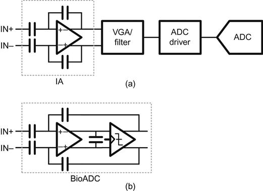
Manipulating functional positioning within the analog block is also very important to maximize the performance while minimizing the power consumption. There are various block-level designs in the analog domain for each application-specific requirement. Separating functions into each block can optimize each function respectively, and maximize programmability on gain and bandwidth [17]. Figure 18(a) shows such an architecture comprising an instrumentation amplifier, a variable-gain/bandwidth amplifier, and an ADC driver, which is connected to an ADC. In contrast to the separation of all functions into each block, the other extreme alternative is an architecture combining all of analog signal conditioning function and analog-to-digital conversion into one block, as shown in Figure 18(b). This architecture removes unnecessary power consumption in the VGA/filter stage and the ADC driver. In addition, it achieves digital controllability in gain and bandwidth by changing duty cycle of integration clock and over-sampling ratio [62].
7.2 Power Domain Design
How the power domains are designed in a system may contribute more to power savings in system performance than improvements by circuit techniques. In most wearable sensors, power is harvested in various ways or supplied from a battery. In any case, the amount of the power is very limited. Therefore, power should be managed wisely. The first step of power management is to design power domains in the system.
Having only one lowest possible power supply in the system is most preferable and does not involve complicated power management schemes and level shifts. However, having different kinds of power levels can be more beneficial in order to reduce the power consumption further. Each block may require different supply voltage, VDD. A block with narrower voltage dynamic range can operate with a lower VDD, resulting in lower power. Higher VDD is necessary for blocks requiring a wide dynamic range. In addition, higher VDD is favorable for better performance in some applications such as a switch, which requires lowest possible turn-on resistance. [78]. In a system with multi-power domains, more careful design is required at the interfaces where different power levels meet. Many techniques such as level shifting, AC-coupling, etc., can be utilized at the interface.
There are several ways to design multi-power domains. 1) A multiple of power levels can be generated directly from the power-harvesting circuit [79]. This method meets different VDD requirements of different blocks and optimizes the power consumptions. However, it requires more complex design in the energy-harvesting block. 2) Multiple power levels can be generated by regulators from a high VDD, which is scavenged or supplied from a battery. This approach can decrease current consumption in some blocks, but the headroom is still wasteful. 3) Contrary to method 2), some higher voltages can be generated from a lower voltage using a power management unit (PMU) such as a charge pump. It can be optimized in terms of power consumption. However, it may induce more complexity because of adding a PMU block [80].
8 Practical Considerations
Outside of controlled laboratory conditions, the largest noise sources will likely be electromagnetic interference (EMI) and movement artifacts. The most common symptom of EMI is seen as 50/60 Hz power line pickup. Triboelectric charging during subject movement is also a large, albeit less understood, source of interference. As a subject moves, the body to environment potential changes due to charge generation as the body strikes the ground. This can couple into the system just like EMI and is often mistaken for movement artifacts due to electrode-skin displacements.
EMI can be reduced or eliminated by a few simple techniques. Common-mode interference is easily attenuated through the use of a DRL. The technique is well understood and operates by actively biasing the body potential towards a fixed circuit reference potential through the use of negative feedback. This has the effect of reducing the magnitude of common mode interference seen by the amplifiers. Differential pickup of EMI is mitigated through the use of active electrodes where an amplifier is placed in close proximity to the electrode. Alternatively, the use of shielded lead wires is also high effective at accomplishing the same goal – minimizing the total area of high impedance traces that are susceptible to external electric fields.
Movement artifacts are a difficult challenge due to the lack of quantified metrics and clear design methodology. Any physical displacement between the electrode and the skin will necessarily generate noise, sometimes many orders of magnitude larger than the actual signal. Movement artifacts can be eliminated by increasing the physical coupling pressure between the electrode and skin, but may conflict with the need for subject comfort and wearability. Reducing movement artifacts highly relies on mechanical and industrial design, and solutions are dependent on the specific end application. In addition, electrode–tissue impedance measurement and signal processing techniques can be used to quantify and suppress movement artifacts [3, 48, 81–86].
9 Conclusion
This chapter reviewed principles of micropower mixed-signal analog and digital integrated circuit design for non-invasive biopotential sensing in wearable clinical and ambulatory physiological monitoring systems. A systematic approach to gm-C circuit design using MOS transistors operating in subthreshold and weak inversion offers high energy and noise efficiency where resolution and bandwidth scale approximately linearly with power consumption. The methodology was illustrated with practical examples of such high-efficiency gm-C MOS circuits for front-end amplification, bandpass filtering, and analog-to-digital conversion. A critical factor in the performance of wearable integrated bioinstrumentation is the electrode-body interface, and practical guidelines of front-end circuit design were given.
Glossary
EEG electroencephalography, electroencephalogram
ECG (EKG) electrocardiography, electrocardiogram
EMG electromyography, electromyogram
MOSFET metal–oxide–semiconductor field-effect transistor
CMOS complementary metal–oxide–semiconductor
BJT bipolar junction transistor
OTA operational transconductance amplifier
ADC analog-to-digital converter
DAC digital-to-analog converter