
Introduction to RF Energy Harvesting
W.A. Serdijn, A.L.R. Mansano and M. Stoopman, Delft University of Technology, Delft, The Netherlands
Radio frequency energy harvesting (RFEH) is an energy conversion technique employed for converting energy from the electromagnetic (EM) field into the electrical domain (i.e., into voltages and currents). In particular, RFEH is a very appealing solution for use in body area networks as it allows low-power sensors and systems to be wirelessly powered in various application scenarios. Extracting energy from RF sources sets a challenging task to designers and researchers as they find themselves at the interface between the electromagnetic fields and the electronic circuitry. Therefore, knowledge from both domains is required in order to design a high-performance RF energy harvester.
In this chapter, the fundamentals, limitations, trade-offs, and challenges of RF energy harvesting are introduced both on system and circuit levels. Several design techniques, such as passive voltage boosting and impedance matching, are presented. State-of-the-art solutions are presented, their advantages and limitations are described, and their figure-of-merit discussed. The rectifier non-linear impedance and performance with respect to frequency, aspect ratio, threshold voltage, loading conditions, and input power variations are discussed. Moreover, the impedance variation introduced by (flexible) antennas for wearable sensors is presented and a technique to overcome the effects of impedance changes is presented.
The choice of the antenna-rectifier interface impedance is discussed as it plays a crucial role in the harvester sensitivity and power conversion efficiency optimization. In the last subsection an example of an RFEH design is furnished, starting from the system level specification requirements of a wearable sensor. Finally, a co-design is described to optimize the antenna-rectifier interface.
Keywords
RF energy harvester; charge pump rectifier; CMOS; antenna; co-design; passive voltage boosting
The ever-decreasing power consumption of integrated circuits provides the opportunity to use an energy harvester to power a simple wireless sensor node. This makes the sensor node truly autonomous and can significantly extend lifetime. With a limited power budget, these sensors are designed to sense, process, and wirelessly transmit information such as temperature, humidity, location, and identification.
In many applications, this power can be supplied by an RF energy harvester when other energy sources such as light, vibrations, and thermal gradients are not available.
Far-field1 radio frequency energy harvesting (RFEH) is suitable for long-range wireless power transfer, i.e., cm range for high-frequency on-chip antennas to several meter range for off-chip antennas. This makes RFEH suitable for battery-less sensors in a WSN remotely powered by a hub (i.e., RF source). RFEH suits many applications, such as smart house, smart grid, Internet of things (IoT), and wireless body area networks (WBAN). Especially in the last few years, the WBAN application is gaining importance due to the growing importance of health care in society as health needs to be continuously monitored to identify chronic diseases or prevent illness. Examples of WBANs are a sensor array for monitoring ExG signals [1–2] and a disposable battery-less band-aid sensor [3].
In WBAN applications, sensors may require power on the order of micro-watts, depending on how they operate. For example, a temperature sensor is not required to update its momentary value very often as temperature is a slowly varying quantity in most applications. On the other hand, the peak power consumption of a duty-cycled sensor might be significantly larger than the harvested (average) power. In such a case, the energy provided by the RFEH can be stored in a capacitor or battery that periodically supplies energy to the sensor. Figure 1 presents the typical energy profile stored in the capacitor and the energy required by the sensor. In this example, the RFEH is periodically connected to a capacitive load, thus efficient energy transfer is required during capacitor charging to minimize losses and charging time. Obviously, the energy supplied by the RFEH over time should be greater than the energy consumed by the sensor.

In this chapter, first RF energy harvesting fundamentals and practical limitations are discussed. Subsequently, an overview is given of different rectifier topologies and circuit implementations with their advantages, disadvantages, and challenges. Then, a compensation scheme is introduced in order to improve the robustness of RF energy harvesters in a practical environment. Finally, an antenna-rectifier co-design example is given to realize a high-performance RF energy harvester. The design is verified by measurements in an anechoic chamber and with energy harvesting from an ambient RF source.
1 RF Energy Harvesting Fundamentals and Practical Limitations
An RF energy harvester designer finds himself at the interface between the electromagnetic radiating fields and the electronic circuitry. In order to optimize this interface for the best possible performance, the designer needs to be equipped with knowledge from both domains. In this section, the basic understanding of antenna fundamental properties and their relationship to power density, impedance, voltage, and current is introduced.
1.1 Wave Propagation, Antenna Effective Area, and Available Power
To understand how the terminal voltage and current of a receiving antenna relate to the radiated power from a transmitting antenna, we start by deriving Friis’ transmission equation. When a signal generator at the transmitter side forces a time-varying current through an antenna structure, electromagnetic radiation is produced as the radiation mechanism of any antenna is based on the acceleration of electric charge. The relative distribution of radiated power in space depends on the radiation pattern. A hypothetical isotropic radiator radiates equally well in all directions such that the power uniformly spreads out across the surface of an imaginary sphere. In reality, antennas radiate and/or receive more effectively in some directions than in others. The directivity ![]() is used to describe the radiation intensity in a given direction compared to the radiation intensity of an isotropic antenna. The power density S [W/m²] at a distance
is used to describe the radiation intensity in a given direction compared to the radiation intensity of an isotropic antenna. The power density S [W/m²] at a distance ![]() from the RF source therefore equals the total radiated power by the transmitter divided by the surface area of a sphere scaled with the directivity of the transmitting antenna [4]:
from the RF source therefore equals the total radiated power by the transmitter divided by the surface area of a sphere scaled with the directivity of the transmitting antenna [4]:
(1)
where ![]() is defined as the equivalent isotropic radiated power (EIRP).
is defined as the equivalent isotropic radiated power (EIRP).
The amount of power collected by a receiving antenna located in the far-field region of the transmitter can be found by using the concept of antenna effective area. The antenna effective area, ![]() , is defined as the ratio of the available power,
, is defined as the ratio of the available power, ![]() , to the power density of a plane wave incident on the antenna:
, to the power density of a plane wave incident on the antenna:
(2)
The available power is defined as the maximum power that can be extracted from an antenna and can be delivered to the load (i.e., power at the input of the RF energy harvester). The actual dissipated power in the antenna load only equals ![]() in case of a lossless and perfectly impedance-matched antenna-electronics interface. For any receiving antenna, it can be proven that the maximum effective antenna area is closely related to its maximum directivity
in case of a lossless and perfectly impedance-matched antenna-electronics interface. For any receiving antenna, it can be proven that the maximum effective antenna area is closely related to its maximum directivity ![]() [4]:
[4]:
(3)
The available power to an RF energy harvester in free space using a lossless and perfectly aligned receiving antenna is then given by
(4)
This equation, known as the Friis’ transmission equation, gives a fundamental limit to the available power as a function of distance, power, frequency, and antenna gain. The ![]() term is often referred to as “free space path loss.” This expression, however, suggests that free space somehow attenuates a propagating electromagnetic wave with decreasing wavelength and increasing distance. This is a misconception. Firstly, the radiated power is not lost over distance, but merely spreads out across the surface area. Secondly, the wavelength enters the equation because of the effective antenna area. A shorter wavelength corresponds to a smaller effective antenna area and therefore is less effective at capturing energy from the incoming wave. In order to capture the same power at a shorter wavelength, the physical area of the antenna needs to be increased.
term is often referred to as “free space path loss.” This expression, however, suggests that free space somehow attenuates a propagating electromagnetic wave with decreasing wavelength and increasing distance. This is a misconception. Firstly, the radiated power is not lost over distance, but merely spreads out across the surface area. Secondly, the wavelength enters the equation because of the effective antenna area. A shorter wavelength corresponds to a smaller effective antenna area and therefore is less effective at capturing energy from the incoming wave. In order to capture the same power at a shorter wavelength, the physical area of the antenna needs to be increased.
1.2 Antenna-Rectifier Interface Voltage
Not only the available power is of concern in the design of RF energy harvesters; the available voltage swing is equally important. This is due to the fact that practical electronic components used for rectification such as diodes and MOS transistors inherently are voltage-controlled devices. Therefore, the first concern in the design of a highly sensitive RF energy harvester is to activate the rectifier by generating a sufficiently large voltage swing at the input of the rectifier.
To link the antenna terminal voltage to the available power, we can use the antenna-rectifier equivalent circuit model as depicted in Figure 2. For now, the antenna impedance is assumed to be purely real for convenience. However, it is also valid to assume that the imaginary part of the antenna impedance is absorbed into the matching network; it does not make a difference for the following analysis.

The voltage and current ratio at the antenna terminals may be modeled by using a Thévenin or Norton equivalent circuit. Here, the voltage induced by the electric field is represented by a Thévenin equivalent voltage source, ![]() . The radiation resistance,
. The radiation resistance, ![]() , relates the voltage and current ratio to the available power. The conduction loss resistance,
, relates the voltage and current ratio to the available power. The conduction loss resistance, ![]() , is related to the antenna radiation efficiency
, is related to the antenna radiation efficiency ![]() by
by
(5)
The total antenna series resistance amounts to ![]() , which corresponds to the real part of the antenna input impedance. The input of the rectifier is modeled as a parallel combination of
, which corresponds to the real part of the antenna input impedance. The input of the rectifier is modeled as a parallel combination of ![]() and
and ![]() . In this model, the power dissipated in
. In this model, the power dissipated in ![]() is seen as the actual power transferred to the (ideal) rectifier DC output port. This resistance is also referred to as a loss-free resistor and becomes useful when modeling an ideal rectifier [5].
is seen as the actual power transferred to the (ideal) rectifier DC output port. This resistance is also referred to as a loss-free resistor and becomes useful when modeling an ideal rectifier [5].
To relate ![]() to
to ![]() , a loss-less and conjugate impedance-matched network is assumed. In this scenario, it follows that
, a loss-less and conjugate impedance-matched network is assumed. In this scenario, it follows that ![]() and
and ![]() . Hence, the power relation for a lossy antenna with conjugate impedance matched interface is written as
. Hence, the power relation for a lossy antenna with conjugate impedance matched interface is written as
(6)
Using (6) and ![]() we can deduce that
we can deduce that
(7)
Equation (7) quickly reveals the expected antenna voltage. As an example, a standard 50 Ω antenna with 90% radiation efficiency and Pav=−20 dBm (10 µW) has an open-circuit terminal voltage of only 60 mV. This is much too low to overcome the threshold voltage of a standard CMOS transistor, which lies around 450 mV in 90 nm IC technology.
The relationship between ![]() and the radiated power of the transmitter is found by substituting (4) into (7):
and the radiated power of the transmitter is found by substituting (4) into (7):
(8)
Note that this general equation holds for any type of antenna. The relations between the antenna equivalent circuit elements are summarized in Table 1.
Table 1
Antenna Equivalent Circuit Elements
| Thévenin equivalent voltage | |
| Radiation resistance | |
| Conduction loss resistance | |
| Antenna resistance | |
| Radiation efficiency |

In general, the antenna voltage ![]() is not the voltage swing at the input of the rectifier. Usually an impedance-matching network transforms the high rectifier input impedance to match with the antenna impedance. This interface impedance transformation can provide a significant passive voltage boost as it increases the voltage swing at the input of the rectifier for the same input power, hence, improving the sensitivity (i.e., power-up threshold) of the RF energy harvester.
is not the voltage swing at the input of the rectifier. Usually an impedance-matching network transforms the high rectifier input impedance to match with the antenna impedance. This interface impedance transformation can provide a significant passive voltage boost as it increases the voltage swing at the input of the rectifier for the same input power, hence, improving the sensitivity (i.e., power-up threshold) of the RF energy harvester.
To calculate the passive voltage boost for a given antenna-electronics interface, the equivalent circuit in Figure 2 again can be used. If the matching network is lossless and assures a conjugate matched interface, then the input power seen from ![]() must equal the power transferred to the rectifier:
must equal the power transferred to the rectifier:
(9)
As ![]() , the passive voltage gain,
, the passive voltage gain, ![]() , is calculated as
, is calculated as
(10)
 (10)
(10)
Note that ![]() is independent of the matching network implementation and only depends on the source and load conditions. Substitution of (10) into (7) leads to the available voltage swing at the rectifier input terminals:
is independent of the matching network implementation and only depends on the source and load conditions. Substitution of (10) into (7) leads to the available voltage swing at the rectifier input terminals:
(11)
Intuitively, this makes sense; for a given antenna radiation efficiency and available input power, the voltage swing can only be increased by increasing the antenna load ![]() . Hence, for an interface with a given source and load resistance, one cannot design for a desired voltage boost to increase wireless range if a conjugate match is required simultaneously. The designer therefore needs to design for the largest
. Hence, for an interface with a given source and load resistance, one cannot design for a desired voltage boost to increase wireless range if a conjugate match is required simultaneously. The designer therefore needs to design for the largest ![]() possible and subsequently co-design the antenna impedance for conjugate matching. This conclusion is a key point that needs to be considered during the design procedure. The rectifier input impedance needs to be designed in such a way that it maximizes the input voltage swing in order to improve the sensitivity.
possible and subsequently co-design the antenna impedance for conjugate matching. This conclusion is a key point that needs to be considered during the design procedure. The rectifier input impedance needs to be designed in such a way that it maximizes the input voltage swing in order to improve the sensitivity.
To elaborate further on the principle of passive voltage boosting, a detailed equivalent antenna-rectifier circuit is depicted in Figure 3. Here, an N-stage rectifier with capacitive load is directly connected to a loop antenna. The reactive element ![]() represents the energy stored in the near field and is inductive since a loop antenna below its first anti-resonance frequency is assumed. By using a loop antenna, the rectifier capacitance can be compensated for without using other external components. The rectifier output is modeled as a Thévenin equivalent circuit. The input impedance of the rectifier is mainly capacitive, where
represents the energy stored in the near field and is inductive since a loop antenna below its first anti-resonance frequency is assumed. By using a loop antenna, the rectifier capacitance can be compensated for without using other external components. The rectifier output is modeled as a Thévenin equivalent circuit. The input impedance of the rectifier is mainly capacitive, where ![]() is the real part of the impedance and
is the real part of the impedance and ![]() represents the imaginary part.
represents the imaginary part.
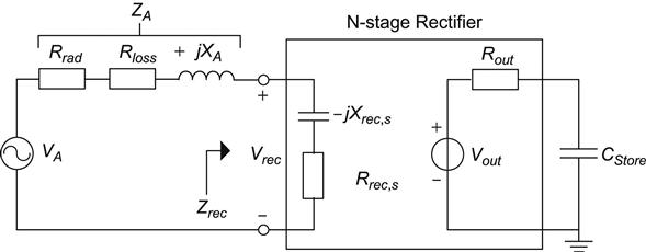
For an N-stage rectifier with a capacitive load, the output voltage in steady state can be written as
(12)
where ![]() is the passive voltage boost obtained from the LC resonating network and
is the passive voltage boost obtained from the LC resonating network and ![]() is the voltage efficiency of a single rectifying stage. When
is the voltage efficiency of a single rectifying stage. When ![]() and the interface is at resonance (
and the interface is at resonance (![]() ), it holds that
), it holds that
(13)
Note that this expression is in a different form compared to (10) and suggests that an increase of ![]() or decrease of
or decrease of ![]() results in a larger passive voltage boost. This indeed corresponds to an increased parallel resistance,
results in a larger passive voltage boost. This indeed corresponds to an increased parallel resistance, ![]() , when performing a series-to-parallel impedance transformation at the frequency of interest:
, when performing a series-to-parallel impedance transformation at the frequency of interest:
(14)
 (14)
(14)
Hence, increasing ![]() or decreasing
or decreasing ![]() (thereby increasing the Q factor and parallel load resistance (
(thereby increasing the Q factor and parallel load resistance (![]() ) results in a larger available voltage swing at the rectifier input terminal.
) results in a larger available voltage swing at the rectifier input terminal.
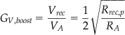
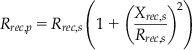
The improvement in sensitivity can be described in terms of the interface impedance, the rectifier properties, and the rectified output voltage. When combining (12) and (13) and using the antenna parameters as given in Table 1, the minimum required available power for a desired ![]() can be written as
can be written as
(15)
From (15), it is evident that the choice of the antenna-rectifier interface impedance plays a crucial role in the optimization of highly sensitive RF energy harvesters. The rectifier input resistance, ![]() , and reactance,
, and reactance, ![]() , depend on the rectifier implementation and decreases with the number of stages N. Increasing the number of stages also indirectly reduces the efficiency due to the body effect when using a standard technology. These issues will be discussed further in the rectifier topology section. If, for example, the design parameters are ηA=0.8, Xrec,s=400 Ω, N=3, and
, depend on the rectifier implementation and decreases with the number of stages N. Increasing the number of stages also indirectly reduces the efficiency due to the body effect when using a standard technology. These issues will be discussed further in the rectifier topology section. If, for example, the design parameters are ηA=0.8, Xrec,s=400 Ω, N=3, and ![]() =0.8, the curves in Figure 4 show the minimum required available power to generate a voltage of 1.5 V across a capacitive load for three different values of
=0.8, the curves in Figure 4 show the minimum required available power to generate a voltage of 1.5 V across a capacitive load for three different values of ![]() as a function of antenna resistance,
as a function of antenna resistance, ![]() .
.

 for ηA=0.8, Xrec,s=400Ω, N=3, and ηV=0.8.
A low resistive antenna-rectifier interface translates into a significant improvement in sensitivity due to the large passive voltage boost, with the minimum of each curve at ![]() . In this particular example, the minimum required available power to generate 1.5 V for a 50 Ω interface equals –11.2 dBm (76.29 µW), while only –19.9 dBm (10.17 µW) is required for a 10 Ω interface, resulting in an 8.7 dB sensitivity improvement.
. In this particular example, the minimum required available power to generate 1.5 V for a 50 Ω interface equals –11.2 dBm (76.29 µW), while only –19.9 dBm (10.17 µW) is required for a 10 Ω interface, resulting in an 8.7 dB sensitivity improvement.
1.3 Practical Limitations
There are several practical limitations that can strongly influence the available DC power for a sensor node during harvesting. The theoretical line-of-sight available power of Eq. (4) can be extended to a more practical form:
(16)
• gain ![]() is a function of the azimuth angle
is a function of the azimuth angle ![]() and the elevation angle
and the elevation angle ![]() and depends on the type of antenna being used;
and depends on the type of antenna being used;
• ![]() is the propagation exponent which can range between 0.8 to 1.8 in a (highly) reflective line-of-sight environment and can get as high as 8.6 for non-line-of-sight environments [6];
is the propagation exponent which can range between 0.8 to 1.8 in a (highly) reflective line-of-sight environment and can get as high as 8.6 for non-line-of-sight environments [6];
• ![]() is the interface impedance mismatch efficiency, where
is the interface impedance mismatch efficiency, where ![]() is the reflection coefficient;
is the reflection coefficient;
• ![]() is the polarization loss factor and depends on the angle
is the polarization loss factor and depends on the angle ![]() between the transmitting and receiving antenna and their polarization; and
between the transmitting and receiving antenna and their polarization; and
• ![]() is the RF-DC power conversion efficiency and highly depends on input power and frequency.
is the RF-DC power conversion efficiency and highly depends on input power and frequency.
2 Impedance Mismatch, Losses, and Efficiency
Impedance mismatch occurs when ![]() or
or ![]() . In such a scenario, the antenna is not able to deliver the full available power to the rectifier. This is a serious concern and requires the designer’s full attention as impedance variations introduced by on-body antennas can strongly degrade the power conversion efficiency. In high-Q interfaces, circuit techniques may be required to automatically tune the interface to minimize impedance mismatch.
. In such a scenario, the antenna is not able to deliver the full available power to the rectifier. This is a serious concern and requires the designer’s full attention as impedance variations introduced by on-body antennas can strongly degrade the power conversion efficiency. In high-Q interfaces, circuit techniques may be required to automatically tune the interface to minimize impedance mismatch.
Additional power loss is introduced by the losses that occur in a practical matching network, the antenna, and the rectifier implementation. The rectifier voltage efficiency, ![]() , can be optimized in an orthogonal way, and usually is on the order of 80% or higher. The power conversion efficiency, PCE, however, highly depends on the rectifier topology and the input power. The radiation efficiency,
, can be optimized in an orthogonal way, and usually is on the order of 80% or higher. The power conversion efficiency, PCE, however, highly depends on the rectifier topology and the input power. The radiation efficiency, ![]() , depends on the antenna size and becomes low when the area is scaled down too much. The (single-stage) rectifier efficiency,
, depends on the antenna size and becomes low when the area is scaled down too much. The (single-stage) rectifier efficiency, ![]() , depends on the components and topology being used.
, depends on the components and topology being used.
2.1 Available Components and Technology
Practical components used for rectification need a minimum voltage in order to conduct current. A typical Schottky diode has a threshold voltage of about 0.3 V, while the threshold voltage of an ordinary diode or a CMOS transistor is usually slightly higher, depending on the technology being used. The minimum required power to reach the rectifier threshold voltage with conjugate matching is given by
(17)
Note that ![]() does not neccesarily equal the diode or transistor threshold voltage, it is also a function of the number of rectifying stages and the circuit topology. For a single Schottky rectifier implementation with equivalent parallel input resistance,
does not neccesarily equal the diode or transistor threshold voltage, it is also a function of the number of rectifying stages and the circuit topology. For a single Schottky rectifier implementation with equivalent parallel input resistance, ![]() =1 kΩ and ηA=0.8, the minimum required power for rectification equals 56.25 µW (–12.5 dBm). The power conversion efficiency will likely be low around this power-up threshold as the diode is just barely forward biased. Typically, the rectifier becomes more efficient for larger input power levels.
=1 kΩ and ηA=0.8, the minimum required power for rectification equals 56.25 µW (–12.5 dBm). The power conversion efficiency will likely be low around this power-up threshold as the diode is just barely forward biased. Typically, the rectifier becomes more efficient for larger input power levels.
If ![]() , for example, can be reduced to 0.1 V, the power-up threshold is lowered to –22 dBm, giving a sensitivity improvement of 9.5 dB. This can be achieved by means of circuit techniques or using more advanced components/technology with low or zero threshold voltage transistors. The latter usually comes at higher costs, so in this case circuit techniques are favorable. Some of these circuit techniques will be discussed in the next section.
, for example, can be reduced to 0.1 V, the power-up threshold is lowered to –22 dBm, giving a sensitivity improvement of 9.5 dB. This can be achieved by means of circuit techniques or using more advanced components/technology with low or zero threshold voltage transistors. The latter usually comes at higher costs, so in this case circuit techniques are favorable. Some of these circuit techniques will be discussed in the next section.
2.2 Regulations and Maximum Achievable Distance
The distance an RF energy harvester can operate from a dedicated RF source is practically determined by the maximum allowed radiated power. The license-free industrial, scientific, and medical (ISM) frequency bands are often used for RF harvesting applications since they allow for high equivalent isotropic radiated power with small antenna areas. Although national restrictions may also apply, the European Radio communications Commission (ERC) limits the maximum ![]() at 868 MHz to 3.28 W and to 4 W at 2.45 GHz [7]. The U.S. Federal Communications Commission (FCC) limits the power levels at the 915 MHz and 2.45 GHz bands to 4 W EIRP [8].
at 868 MHz to 3.28 W and to 4 W at 2.45 GHz [7]. The U.S. Federal Communications Commission (FCC) limits the power levels at the 915 MHz and 2.45 GHz bands to 4 W EIRP [8].
As a practical example, Figure 5 shows the available DC power versus distance when transmitting the maximum allowed power in the European 868 MHz band. A line-of-sight scenario is assumed where PEIRP=3.28 W, λ=0.345 m, GA=1.25, ![]() =0.9, and
=0.9, and ![]() =0.8. The available power is shown for both a power conversion efficiency (PCE) of 50% and 100%. The power-up threshold creates an upper limit to the maximum achievable range. In this scenario, a reduction in rectifier threshold voltage from 0.3 V to 0.1 V increases the maximum achievable distance from 5 meters to 14.7 meters for ηPCE=50%. This indicates the importance of minimizing
=0.8. The available power is shown for both a power conversion efficiency (PCE) of 50% and 100%. The power-up threshold creates an upper limit to the maximum achievable range. In this scenario, a reduction in rectifier threshold voltage from 0.3 V to 0.1 V increases the maximum achievable distance from 5 meters to 14.7 meters for ηPCE=50%. This indicates the importance of minimizing ![]() in case the regulations do not allow increasing the radiated power.
in case the regulations do not allow increasing the radiated power.

3 Distribution of Harvested Power in a Realistic Environment
The harvested power can vary significantly in a realistic environment due to the many unknown variables in the propagation channel. Figure 6 shows the measured harvested power in an office room (~24 m²) for three different scenarios using a Powercast P2110-EVAL-02 RF energy harvesting development kit at a 3.5 meter distance from the 3 W EIRP dedicated RF source. In each scenario, 1,000 samples are taken over a period of 30 minutes.

The first figure shows a static office environment with line-of-sight and aligned antenna. The mean value is –11.26 dBm with a standard deviation of 0.57 dBm. A scenario shown in Figure 6(b) demonstrates harvested power in a case with random line-of-sight angular and lateral misalignment. Here, a mean value of –13.7 dBm was measured with a standard deviation of 3.86 dBm. The last scenario is non-line-of-sight with random misaligned antennas in a highly dynamic office room with people walking in between the transmitter and RF harvester. The mean value is –17.86 dBm with a standard deviation of 4.67 dBm. Although these measurements strongly depend on the environment and the RFEH, they demonstrate that the available power can vary significantly. These fluctuations need to be considered at system level. Moreover, these measurements also demonstrate the need for an intelligent RF source that tracks the sensor node and steers the highly directive beam towards the sensor to always provide sufficient available power to the RF harvester in any given scenario.
3.1 Ambient RF Power
Harvesting RF energy from ambient sources such as TV, GSM, and WLAN base stations sounds very promising as these signals are omnipresent in urban environments and open the possibility to realize truly autonomous wireless sensors. Unfortunately, this is only feasible for a limited number of applications as the available power generally is very low and unreliable. In [9], an experiment was conducted to measure the received signal strength and probability in an urban and suburban area between 800 and 900 MHz. In an urban area, the received signal strength was most likely around –20 to –40 dBm with a peak probability of 31% around –33 dBm. In a less densely populated environment, this peak was around –37 dBm with a probability of 27%. Similar results have been found in [10], where the ambient RF energy available from a GSM-900 cell was found to be on the order of –30 dBm at 200 m distance. These power levels are generally considered to be too low to be used for RF harvesting as they are around or below the power-up threshold.
4 Charge Pump Rectifier Topologies
Rectifiers are very well known as power conversion devices that convert alternating current (AC) to direct current (DC). In the beginning of the twentieth century, rectifiers were usually applied to high-voltage and high-power applications. The same principal of rectifying current and voltage can be applied to RF energy harvesting, where rectifiers convert AC power, captured by an antenna, to DC power that is subsequently delivered to a load. Generally, the rectified voltage is also boosted to achieve higher levels. Thus, the rectifier also operates as a charge pump, and for this reason, the term charge pump rectifier (CPR) is commonly found in RFEH literature.
An example of a CPR is presented in Figure 7. This is one of the simplest CPR topologies, and comprises only diodes and capacitors. In the positive half-period of a sinusoidal voltage applied across the anode-cathode junction, the diode conducts current and thus transfers charge to the capacitor connected at the cathode terminal, which stores this charge, thereby producing or increasing its DC voltage. Since the circuit has two diodes, the voltage is rectified in both semi-cycles. The diode can be seen as a switch with a voltage source (VD) in series. The equivalent circuits in both half-periods are represented in Figure 8 (a) and (b). The diodes have losses, represented by VD, that limit the CPR output voltage and, consequently, the power conversion efficiency (PCE). The steady-state output voltage of this topology is described by (18), where VIN is the input peak voltage:
(18)


As can be noticed (18), VD is an undesired factor and has to be minimized for better power conversion.
Various techniques and topologies that have been developed to reduce VD, and increase PCE and the sensitivity of CPRs, will be briefly discussed here. A Schottky diode is a special type of diode built on a metal-semiconductor substrate which has low VD (0.15 V – 0.4 V) [11,12]. One approach is the replacement of conventional diodes, in the circuit of Figure 7, by Schottky diodes. The circuit topology is not different from Figure 7; the significant change is in the reduction of diode voltage drop.
The advantage of diodes is that they conduct current in one direction only, thus, no flow-back current losses are associated with the use of diodes in case the CPR receives high voltage levels. The main drawback of Schottky diodes is their manufacturing cost. Therefore, these diodes are not always available in CMOS technologies because their use adds to the costs considerably.
Due to the costs and processing disadvantages of Schottky diodes, many research groups have been looking into solutions to reduce CPR losses using standard CMOS processes. An integrated CMOS rectifier has a clear advantage over discrete Schottky diodes as MOS transistors can easily be scaled and have four terminals compared to two terminal diodes. This allows for a much more versatile design approach with many different topology and circuit techniques to design for the optimum rectifier input impedance.
The CPR in Figure 9(a) replaces diodes by MOS transistors connected as diodes. However, MOS transistors also present a voltage drop, which depends on the threshold voltage (VTH) of the MOS transistor. For this reason, techniques to reduce the threshold voltage have been developed. A known technique is the floating gate threshold voltage compensation [13]. This technique consists of MOS transistors connected as diodes with a capacitor connected between the drain and gate terminals. Assuming the initial voltages on these capacitors are zero, before operation, the capacitors must be charged with a voltage close to VTH. After that, the diode-connected transistors will have their conduction losses reduced since the capacitors work as series voltage sources, as shown in Figure 9(b), and thus drive the gates with higher voltages. The extra voltage allows the transistor channel to be inverted with lower gate-source voltages, thereby minimizing VTH effects.

The advantages of this topology are good VTH compensation and simple circuit implementation. On the other hand, the pre-charging of the capacitors needs to be accurate in order to avoid excessive extra potential, which can lead to negative turn-on voltages. As a consequence, losses due to flow-back current become very significant. Moreover, pre-charging requires a battery, thus, making this technique unattractive to truly autonomous solutions.
Other techniques for VTH compensation are presented in Figure 10 (a)–(c)[14–16]. In Figure 10 (a) the compensation relies on the output voltages of the succeeding stages that are fed back to the compensated stage. This method does not require pre-charging of the gates, and the circuit implementation has moderate complexity. However, it requires a large amount of stages to provide enough voltage for compensation. In the technique presented in Figure 10(b) the threshold voltage of MN1 is reduced by a biasing circuit. MN2 conducts current that is limited by R1, and a gate-source voltage is produced across MN2. The gate-source voltage of MN2 sets a lower threshold voltage to MN1. For MP2 the threshold compensation is similar to MN1. This technique also requires a large amount of stages and it needs extra components, such as resistors and capacitors, to build the compensation scheme. In both approaches, flow-back current may also increase losses at high input power. Figure 10(c) shows a technique that employs an auxiliary CPR chain for VTH compensation. The compensation is very effective, but chip area is significantly increased and the received power is divided between the main and auxiliary chain.

Another technique found in the literature comprises dynamic VTH compensation and voltage boosting to assist the MOS transistors switching on/off [17]. Figure 11 shows the principle diagram consisting of a boosting network and a charge pump rectifier. The CPR is connected to four branches provided by a boosting network. The signals Vb+ and Vb– are the switching signals, and Vr+ and Vr– are connected to the input of the rectifier. Figure 12 (a) and (b) present the details of the boosting network and one stage of the rectifier circuit. Note that the PMOS transistors in Figure 12(b) are set to operate as voltage-controlled switches to reduce voltage drops. In each stage, the output voltage is fed back to the transistor gate through RDC and CDC. Capacitor CC couples the AC voltage from the boosting network to the gate of the PMOS. As a result, the PMOS gate voltage has two components, one DC component for threshold compensation, and one AC component to turn on/off the transistors in the positive/negative half-periods. The advantages of this topology are reduced number of stages, no pre-charging, and reduced flow-back losses. On the other hand, the circuit implementation is more complex and its efficiency depends on the boosting network quality factor. Considering that the other techniques require a matching network as well, the quality factor will also affect their efficiency. A comparison among the various approaches can be found in [17].


5 Effect of Load and Source Variations
In the previous section, CPR topologies and techniques to improve efficiency/sensitivity were presented. This section discusses how CPR efficiency (PCE) and impedance (ZIN) are affected by load variations and input power deviations.
Let us assume that a resistive load is connected to the output of the CPR. As the input power increases, the input voltage is expected to increase, thus the output voltage also increases. Since the load is a constant resistance, the output current also increases. The output current is reflected to the input as more charge needs to be transferred to the capacitors of the rectifier and, as a result, the input current increases. Despite an input voltage and current increase, it is hard to affirm whether the rectifier input impedance increases or decreases since the voltage-to-current ratio is highly nonlinear. Thus, ZIN tendency should be determined by transient simulations or measurements in order to reach a more accurate estimation. Analytical analysis can also be performed. However, it is less accurate as mathematical reduction is usually applied to simplify the analysis.
Besides input power deviation, load deviation also affects input impedance and efficiency. The PCE and ZIN as a function of load impedance are nonlinear and change with topology and VTH compensation. In Figure 13 efficiency vs input power (PIN) for a constant resistive load is depicted. Most of the topologies presented in this section have similar behavior to the plot of Figure 13. As PIN increases, PCE increases until a maximum point, and drops as PIN further increases. Changes in ZIN, voltage drop losses, and flow-back losses are the factors that cause the PCE to drop. In addition, the differences among technologies, topologies, and compensation schemes cause differences in peak efficiency, minimum PCE, and sensitivity.

5.1 Optimum Power Transfer Techniques
The concept of high-Q passive voltage boosting to improve sensitivity has the disadvantage that the antenna-rectifier interface becomes very sensitive to small impedance variations. These variations can be the result of process mismatch, variation in input power level, or environment changes caused by on-body antennas. This is extensively reported in various articles on printed flexible antennas [18–20]. Also, the rectifier nonlinearity presents a challenging task to the designer. A robust RF energy harvester therefore requires a mechanism that compensates for these effects. A well-known compensation method used in various applications is maximum power point tracking (MPPT), as proposed in [21,22]. MPPT optimizes the DC-DC energy transfer after the rectification is performed. Another possible solution to this problem is to adjust the antenna-rectifier interface impedance using a resonance control loop as shown in Figure 14 [23,24].

The principle of the control loop is the following: after the harvester initially charges the storage capacitor, CSTORE, to the turn-on voltage of the loop, the slope information of ![]() is obtained using a differentiating network. Subsequently, a sample and comparator stage compares the slope information of
is obtained using a differentiating network. Subsequently, a sample and comparator stage compares the slope information of ![]() with the previous sample and determines if the slope has increased or decreased. This information is fed to a finite-state machine that determines if the up-down counter should keep counting or change count direction. The output of the n-bit up-down counter is used to control an n-bit binary weighted capacitor bank at the interface. This way, the control loop continuously maximizes the slope of
with the previous sample and determines if the slope has increased or decreased. This information is fed to a finite-state machine that determines if the up-down counter should keep counting or change count direction. The output of the n-bit up-down counter is used to control an n-bit binary weighted capacitor bank at the interface. This way, the control loop continuously maximizes the slope of ![]() , corresponding to maximum energy transfer with minimum charging time. Once the loop is calibrated, it can be turned off so that it is not loading the rectifier for very low power levels.
, corresponding to maximum energy transfer with minimum charging time. Once the loop is calibrated, it can be turned off so that it is not loading the rectifier for very low power levels.
The core of the harvester consists of a conventional n-stage cross-connected bridge rectifier. In this structure, the output voltage and common-mode gate voltage generated during rectification provide additional biasing and effectively reduce the required turn-on voltage. Due to this VTH self-cancellation, the rectifier can be activated at lower input power levels than other similar topologies. Another benefit is its symmetry, as this circuit cancels all even order harmonic currents that can be re-radiated, and therefore improves power efficiency. The required transistor width is determined by analyzing the charging time and input impedance for different input voltages when changing the transistor width. Then, a trade-off is made between minimum charging time, maximum voltage boost, and output voltage (i.e., number of stages).
The capacitor bank consists of ![]() unit capacitor switches, where each unit consists of a main switching transistor, two small biasing transistors to enhance the Q-factor, and two custom-designed metal-metal capacitors. The desired tuning range and accuracy can be set with the number of bits. A low-dropout regulator (LDO) offers a stable supply voltage for the control loop. The required bandwidth of the loop is on the order of kHz as the charging time is relatively slow. Because of this, the average power consumption of the mainly digital loop can be designed with negligible power consumption.
unit capacitor switches, where each unit consists of a main switching transistor, two small biasing transistors to enhance the Q-factor, and two custom-designed metal-metal capacitors. The desired tuning range and accuracy can be set with the number of bits. A low-dropout regulator (LDO) offers a stable supply voltage for the control loop. The required bandwidth of the loop is on the order of kHz as the charging time is relatively slow. Because of this, the average power consumption of the mainly digital loop can be designed with negligible power consumption.
The resonance control loop optimization is verified with simulations and shown in Figure 15(a) for Pav=−20 dBm using a relatively small load capacitance of 10 pF in order to reduce simulation time. The binary “CountDirection” is the output signal of the finite-state machine that controls the up-down count direction. The control loop keeps counting up or down (depending on the initial direction) as long as the slope of ![]() keeps increasing. The slope decreases when the capacitor bank has passed the optimum capacitance. In this case, “CountDirection” turns from “1” to “0” and the loop inverts the counting direction. At the optimum capacitance code, “CountDirection” oscillates between “1” and “0” at the clock frequency.
keeps increasing. The slope decreases when the capacitor bank has passed the optimum capacitance. In this case, “CountDirection” turns from “1” to “0” and the loop inverts the counting direction. At the optimum capacitance code, “CountDirection” oscillates between “1” and “0” at the clock frequency.

This scheme ensures that small impedance variations, which may occur in a realistic environment, will be compensated for by the control loop, making the RF energy harvester very robust while it benefits from the passive voltage boost obtained from the high-Q antenna. This is demonstrated in Figure 15(b), where the antenna inductance is varied between 80 nH ![]() 160 nH to mimic antenna environment changes. The control loop is able to cope with these large variations despite the high-Q antenna network and maximizes
160 nH to mimic antenna environment changes. The control loop is able to cope with these large variations despite the high-Q antenna network and maximizes ![]() in each scenario.
in each scenario.
6 Antenna-Rectifier Co-Design
Co-designing the antenna with the rectifier allows optimization of the performance as the interface is no longer constrained by the traditional 50 Ω characteristic. The design methodology described in this section requires a highly inductive antenna that is conjugate matched to the rectifier input impedance. This antenna impedance can be realized using a modified folded dipole antenna as depicted in Figure 16. This compact loop antenna has additional short-circuited arms in order to fine-tune the antenna impedance.

A prototype antenna is designed and fabricated on 1.6 mm FR4 substrate. The antenna impedance is simulated in CST Microwave Studio using frequency, transient, and transmission line solvers, and all converge to approximately 11+j398.8 Ω at 868 MHz, thereby ensuring a high degree of confidence in the simulation procedure and accuracy. The radiation efficiency and maximum directivity of this prototype antenna is 46.5% and 1.55 dBi, respectively. This corresponds to a maximum antenna gain of –1.78 dBi.
The rectifier chip is integrated on the back side of the antenna to minimize its effect on the antenna performance. The RF inputs are bond wired to vias (2 mm in diameter) that connect to the antenna feed point. The other control signals are connected to a control logic and measurement board to evaluate the performance. All off-chip connections (vias, bondwires, PCB traces, connector) are included in the antenna simulations to accurately determine the input impedance at the antenna feedpoint (Figure 17).

6.1 Measurements and Verification
At the end of the design and fabrication phase, the performance needs to be evaluated by verifiable measurements. This way, the performance can be compared properly to the state of the art. For this reason, the RF harvester first is measured in an anechoic chamber to mimic a free-space condition. The setup (Figure 18) is calibrated at 868 MHz using two identical broadband log periodic antennas (HG824–11LP-NF) separated by 3.6 meters to ensure far-field conditions. Since the harvesting antenna dimensions (a=λ/11.3 and c=λ/9.8) are much smaller than the wavelength, the antenna performance is included in the measurements by defining the available input power as the maximum power available from an isotropic antenna (GA=0 dBi). Using this definition, the RF-DC power conversion efficiency is defined as
(19)

This isotropic available power is determined by measuring the received power using the reference antenna at the harvester position and subsequently adding the reference antenna gain to obtain ![]() . The measured power is within ±0.5 dB agreement with the theoretical available power calculated from (4). As the control loop is off-chip, its power consumption during calibration is not included in the measurements.
. The measured power is within ±0.5 dB agreement with the theoretical available power calculated from (4). As the control loop is off-chip, its power consumption during calibration is not included in the measurements.
To demonstrate the adaptability of the resonance control loop, the measured output voltage for closed and open-loop scenarios is shown in Figure 19(a), where Rload=1 MΩ and Pin=−20 dBm. During a capacitance sweep (open loop), the control loop is continuously counting from the minimum to the maximum capacitance value. Clearly, an optimum capacitance exists that corresponds to maximum power. In the closed-loop scenario, the loop optimization is activated at 0.5 seconds and maximizes the power dissipation in the load. The charging time vs. PIN for a 450 nF load capacitance is shown in Figure 19(b).


The measured ![]() vs. input power is depicted in Figure 20(a) and shows an excellent sensitivity for low power levels. A capacitor can be charged to 1 V with only –26.3 dBm input power and takes approximately 2 seconds for a 450 nF capacitor. As the charging time scales linearly with the capacitor size, these graphs give a good indication of the available energy as a function of input power and time.
vs. input power is depicted in Figure 20(a) and shows an excellent sensitivity for low power levels. A capacitor can be charged to 1 V with only –26.3 dBm input power and takes approximately 2 seconds for a 450 nF capacitor. As the charging time scales linearly with the capacitor size, these graphs give a good indication of the available energy as a function of input power and time.


Figure 20 (b) shows that the power efficiency peaks around –15 dBm with a maximum of 31.5%. This includes all losses of the antenna, interface, and rectifier.
To verify the performance in a realistic environment, the RF harvester is tested for both a dedicated and ambient RF source. First, a dedicated 1.78 W EIRP RF source was used to measure the line-of-sight distance in an office corridor. In this experiment, 1 V could be generated from a 25-meter distance, corresponding well with –26.3 dBm sensitivity. The energy harvesting from ambient RF sources is demonstrated by measuring the output voltage when using a GSM-900 mobile phone from a 2-meter distance (Figure 21). Although the frequency and power levels varied greatly during a call (peak power levels of –4.6 dBm were measured between 886 MHz and 907 MHz), the RF harvester was able to charge a capacitor to 2.2 V. Both experiments demonstrate the feasibility of RF energy harvesting for a wide range of applications.

7 Conclusion
RF energy harvesting is an increasingly popular research topic that has gained a lot of attention since the introduction of RFID, autonomous wireless sensors, and wearable devices. RF energy harvesting fundamentals such as wave propagation, antenna efficiency, and antenna-rectifier interface have been presented. It has been shown that the choice of antenna-rectifier interface impedance plays a crucial role in the optimization of highly sensitive RF energy harvesters.
Practical limitations, which include impedance mismatch, losses, government regulations, and harvested-power distribution in realistic environments, affect RF energy-harvesting performance and must be taken into account in the design during the specification phase. Rectifier topologies and techniques for reducing losses have been presented. One simple scheme is a rectifier consisting of Schottky diodes and capacitors. Despite great reduction of power losses, Schottky diodes are expensive and are not available in most IC technologies. Therefore, CMOS-based solutions have been developed by many research groups to align low process cost with good performance.
Besides rectifier topologies, optimum power transfer techniques were introduced to increase sensitivity and efficiently transfer energy from antenna to rectifier. An example of an RFEH employing antenna-rectifier co-design has been shown and measurement results have been presented. A peak efficiency of 31.5% has been achieved at –15 dBm, showing state-of-the-art performance of the RF energy harvesting by employing a resonance control loop.
The fundamental RF energy harvesting properties, challenges, techniques, and design procedures covered in this section give the designer the essential knowledge to optimize and realize high-performance RF energy harvesters for wearable device applications.
Acknowledgement
The authors gratefully acknowledge the technical and financial support provided by IMEC-NL/Holst centre at Eindhoven, the Netherlands and Conselho Nacional de Desenvolvimento Científico e Tecnológico (CNPq), Brazil.