
Chapter 4. Motherboards and Buses
Motherboard Form Factors
Without a doubt, the most important component in a PC system is the main board or motherboard. Virtually every internal component in a PC connects to the motherboard, and its features largely determine what your computer is capable of, not to mention its overall performance. Although I prefer the term motherboard, other terms such as main board, system board, and planar are interchangeable. This chapter examines the various types of motherboards available and those components typically contained on the motherboard and motherboard interface connectors.
Several common form factors are used for PC motherboards. The form factor refers to the physical dimensions (size and shape) as well as certain connector, screw hole, and other positions that dictate into which type of case the board will fit. Some are true standards (meaning that all boards with that form factor are interchangeable), whereas others are not standardized enough to allow for interchangeability. Unfortunately, these nonstandard form factors preclude any easy upgrade or inexpensive replacement, which generally means they should be avoided. The more commonly known PC motherboard form factors include the following:
Obsolete Form Factors
• Baby-AT (PC and XT)
• Full-size AT
• LPX (semiproprietary)
• NLX
• WTX
• BTX, microBTX, picoBTX
Modern Form Factors
• ATX and variants; microATX, FlexATX, DTX/Mini-DTX, and ITX/Mini-ITX
PC motherboard form factors have evolved over the years from the Baby-AT form factor boards based on the original IBM PC and XT, to the current ATX form factor (and variants) used in most desktop and tower systems. ATX has a growing number of variants, mostly in smaller sizes designed to fit different market segments and applications. The short-lived BTX form factors relocated major components to improve system cooling and incorporate a thermal module.
Anything that does not fit into one of the industry-standard form factors should be considered proprietary. Unless there are special circumstances, I do not recommend purchasing systems based on proprietary board designs because they are difficult to upgrade and expensive to repair because components such as the motherboard, case, and power supply are not interchangeable with other systems. I often call proprietary form factor systems “disposable” PCs because that’s what you must normally do with them when they are too slow or need repair out of warranty.
Obsolete Form Factors
The following sections examine industry-standard motherboard form factors no longer in use, but which can be commonly found on older systems.
PC and XT
The first popular PC motherboard was, of course, the original IBM PC released in August 1981. Figure 4.1 shows how this board looked. IBM followed the PC with the XT motherboard in March 1983, which had the same size and shape as the PC board but had eight slots instead of five. Both the IBM PC and XT motherboards were 9″×13″ in size. Also, the slots were spaced 0.8″ apart in the XT instead of 1″ apart as in the PC (see Figure 4.2). The XT also eliminated the little-used cassette port in the back, which was supposed to be used to save BASIC programs on cassette tape instead of the much more expensive (at the time) floppy drive.
Figure 4.1 IBM PC motherboard (circa 1981).
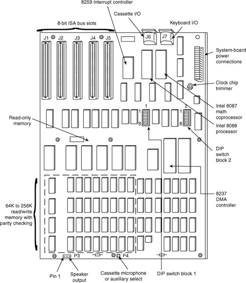
Figure 4.2 IBM PC-XT motherboard (circa 1983).

Note
The Technical Reference section of the disc accompanying this book contains detailed information on the PC (5150) and XT (5160). All the information there is printable.
The minor differences in the slot positions and the deleted cassette connector on the back required a minor redesign of the case. In essence, the XT was a mildly enhanced PC, with a motherboard that was the same overall size and shape, used the same processor, and came in a case that was identical except for slot bracketry and the lack of a hole for the cassette port. Eventually, the XT motherboard design became very popular, and many other PC motherboard manufacturers of the day copied IBM’s XT design and produced similar boards.
Full-Size AT
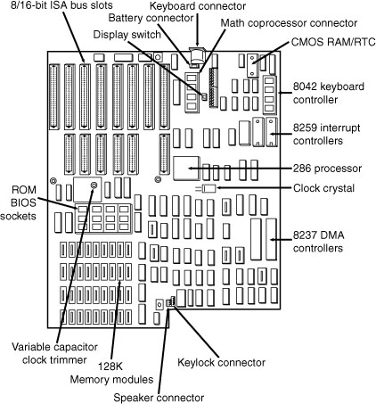
The full-size AT motherboard form factor matches the original IBM AT motherboard design. This allows for a very large board of up to 12″ wide by 13.8″ deep. The full-size AT board first debuted in August 1984, when IBM introduced the Personal Computer AT (advanced technology). To accommodate the 16-bit 286 processor and all the necessary support components at the time, IBM needed more room than the original PC/XT-sized boards could provide. So for the AT, IBM increased the size of the motherboard but retained the same screw hole and connector positions of the XT design. To accomplish this, IBM essentially started with a PC/XT-sized board and extended it in two directions (see Figure 4.3).
Figure 4.3 IBM AT motherboard (circa 1984).
Note
The Technical Reference section of the disc enclosed with this book contains detailed coverage of the AT and the XT Model 286.
A little more than a year after being introduced, the appearance of chipsets and other circuit consolidation allowed the same motherboard functionality to be built using fewer chips, so the board was redesigned to make it slightly smaller. Then, it was redesigned again as IBM shrank the board down to XT-size in a system it called the XT-286 (introduced in September 1986). The XT-286 board was virtually identical in size and shape to the original XT, a form factor which would later be known as Baby-AT.
The keyboard connector and slot connectors in the full-size AT boards still conformed to the same specific placement requirements to fit the holes in the XT cases already in use, but a larger case was still required to fit the larger board. Because of the larger size of the board, a full-size AT motherboard only fits into full-size AT desktop or tower cases. Because these motherboards do not fit into the smaller Baby-AT or mini-tower cases, and because of advances in component miniaturization, they are no longer being produced by most motherboard manufacturers—except in some cases for dual processor server applications.
The important thing to note about the full-size AT systems is that you can always replace a full-size AT motherboard with a Baby-AT (or XT-size) board, but the opposite is not true unless the case is large enough to accommodate the full-size AT design.
Baby-AT
After IBM released the AT in August 1984, component consolidation allowed subsequent systems to be designed using far fewer chips and requiring much less in the way of motherboard real estate. Therefore, all the additional circuits on the 16-bit AT motherboard could fit into boards using the smaller XT form factor.
The Baby-AT form factor is essentially the same form factor as the original IBM XT motherboard. The only difference is a slight modification in one of the screw hole positions to fit into an AT-style case. These motherboards also have specific placement of the keyboard and slot connectors to match the holes in the case. Note that virtually all full-size AT and Baby-AT motherboards use the standard 5-pin DIN type connector for the keyboard. Baby-AT motherboards can be used to replace full-size AT motherboards and will fit into several case designs. Because of its flexibility, from 1983 into early 1996, the Baby-AT form factor was the most popular motherboard type. Starting in mid-1996, Baby-AT was replaced by the superior ATX motherboard design, which is not directly interchangeable. Figure 4.4 shows the onboard features and layout of a late-model Baby-AT motherboard.
Figure 4.4 A late-model Baby-AT motherboard, the Tyan Trinity 100AT (S1590). Photo courtesy of Tyan Computer Corporation.

The easiest way to identify a Baby-AT form factor system without opening it is to look at the rear of the case. In a Baby-AT motherboard, the cards plug directly into the board at a 90° angle; in other words, the slots in the case for the cards are perpendicular to the motherboard. Also, the Baby-AT motherboard has only one visible connector directly attached to the board, which is the keyboard connector. Typically, this connector is the full-size 5-pin DIN type connector, although some Baby-AT systems use the smaller 6-pin mini-DIN connector (sometimes called a PS/2-type connector) and might even have a mouse connector. All other connectors are mounted on the case or on card edge brackets and are attached to the motherboard via cables. The keyboard connector is visible through an appropriately placed hole in the case.
![]() See “Keyboard/Mouse Interface Connectors,” p. 814 (Chapter 15, “Input Devices”).
See “Keyboard/Mouse Interface Connectors,” p. 814 (Chapter 15, “Input Devices”).
Baby-AT boards all conform to specific widths and screw hole, slot, and keyboard connector locations, but one thing that can vary is the length of the board. Versions have been built that are smaller than the full 9″×13″ size; these are often called mini-AT, micro-AT, or even things such as 2/3-Baby or 1/2-Baby. Even though they might not be the full size, they still bolt directly into the same case as a standard Baby-AT board and can be used as a direct replacement for one.
LPX
The LPX and mini-LPX form factor boards were a semiproprietary design that Western Digital originally developed in 1987 for some of its motherboards. The LP in LPX stands for Low Profile, which is so named because these boards incorporate slots that are parallel to the main board, enabling the expansion cards to install sideways. This allows for a slim or low-profile case design and overall a smaller system than the Baby-AT.
Although Western Digital no longer produces PC motherboards, the form factor lives on, and many other motherboard manufacturers have duplicated the general design. Unfortunately, because the specifications were never laid out in exact detail—especially with regard to the bus riser card portion of the design—these boards are termed semiproprietary and are not interchangeable between manufacturers. Some vendors, such as IBM and HP, for example, have built LPX systems that use a T-shaped riser card that allows expansion cards to be mounted at the normal 90° angle to the motherboard but still above the motherboard. This lack of standardization means that if you have a system with an LPX board, in most cases you can’t replace the motherboard with a different LPX board later. You essentially have a system you can’t upgrade or repair by replacing the motherboard with something better. In other words, you have what I call a “disposable PC,” something I would not normally recommend that anybody purchase.
Most people were not aware of the semiproprietary nature of the design of these boards, and they were extremely popular in what I call “retail store” PCs from the late 1980s through the late 1990s. This would include primarily Compaq and Packard Bell systems, as well as many others who used this form factor in their lower-cost systems. These boards were most often used in low-profile or Slimline case systems, but were found in tower cases too. These were often lower-cost systems such as those sold at retail electronics superstores. LPX is considered obsolete today.
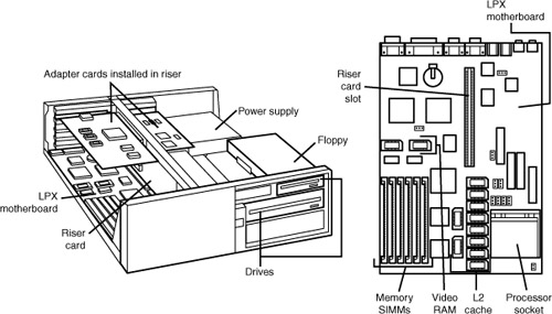
LPX boards are characterized by several distinctive features (see Figure 4.5). The most noticeable is that the expansion slots are mounted on a bus riser card that plugs into the motherboard. In most designs, expansion cards plug sideways into the riser card. This sideways placement allows for the low-profile case design. Slots are located on one or both sides of the riser card depending on the system and case design. Vendors who use LPX-type motherboards in tower cases sometimes use a T-shaped riser card instead, which puts the expansion slots at the normal right angle to the motherboard but on a raised shelf above the motherboard itself.
Figure 4.5 Typical LPX system chassis and motherboard.
Another distinguishing feature of the LPX design is the standard placement of connectors on the back of the board. An LPX board has a row of connectors for video (VGA 15-pin), parallel (25-pin), two serial ports (9-pin each), and mini-DIN PS/2-style mouse and keyboard connectors. All these connectors are mounted across the rear of the motherboard and protrude through a slot in the case. Some LPX motherboards might have additional connectors for other internal ports, such as network or SCSI adapters. Because LPX systems use a high degree of motherboard port integration, many vendors of LPX motherboards, cases, and systems often refer to LPX products as having an “all-in-one” design.
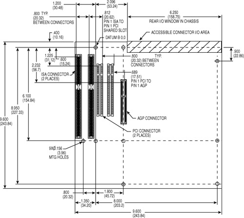
The standard form factor used for LPX and mini-LPX motherboards in many typical low-cost systems is shown in Figure 4.6.
Figure 4.6 LPX motherboard dimensions.

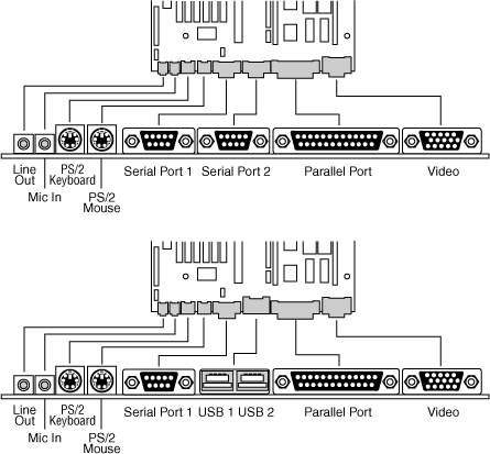
I am often asked, “How can I tell whether a system has an LPX board without opening the cover?” Because of the many variations in riser card design, and because newer motherboards such as NLX also use riser cards, the most reliable way to distinguish an LPX motherboard from other systems is to look at the connector signature (the layout and pattern of connectors on the back of the board). As you can see in Figure 4.7, all LPX motherboards—regardless of variations in riser card shape, size, or location—place all external ports along the rear of the motherboard. By contrast, Baby-AT motherboards use case-mounted or expansion slot-mounted connectors for serial, parallel, PS/2 mouse, and USB ports, whereas ATX-family and BTX-family motherboards group all external ports together to the left side of the expansion slots.
Figure 4.7 LPX motherboard back panel connectors.
On an LPX board, the riser is placed in the middle of the motherboard, whereas NLX boards have the riser to the side (the motherboard actually plugs into the riser in NLX).
Figure 4.7 shows two typical examples of the connectors on the back of LPX boards. Note that not all LPX boards have the built-in audio, so those connectors might be missing. Other ports (such as USB) might be missing from what is shown in these diagrams, depending on exactly which options are included on a specific board; however, the general layout will be the same.
The connectors along the rear of the board would interfere with locating bus slots directly on the motherboard, which accounts for why riser cards are used for adding expansion boards.
NLX
NLX is a low-profile form factor designed to replace the nonstandard LPX design used in previous low-profile systems. First introduced in November 1996 by Intel, NLX was a popular form factor in the late 1990s for Slimline corporate desktop systems from vendors such as Compaq, HP, Toshiba, and others. Since 2000, many Slimline systems have used variations on the FlexATX motherboard instead.
NLX is similar in initial appearance to LPX, but with numerous improvements designed to enable full integration of the latest technologies. NLX is basically an improved version of the proprietary LPX design, but, unlike LPX, NLX is fully standardized, which means you should be able to replace one NLX board with another from a different manufacturer—something that was not possible with LPX.
Another limitation of LPX boards is the difficulty in handling the larger physical size of the newer processors and their larger heatsinks, as well as newer bus structures such as AGP for video. The NLX form factor has been designed specifically to address these problems (see Figure 4.8). In fact, NLX provides enough room for some vendors to support dual Slot 1 Pentium III processors in this form factor.
Figure 4.8 NLX motherboard and riser combination.

The main characteristic of an NLX system is that the motherboard plugs into the riser, unlike LPX where the riser plugs into the motherboard. Therefore, the motherboard can be removed from the system without disturbing the riser or any of the expansion cards plugged into it. In addition, the motherboard in a typical NLX system literally has no internal cables or connectors attached to it! All devices that normally plug into the motherboard—such as drive cables, the power supply, the front panel light, switch connectors, and so on—plug into the riser instead (see Figure 4.8). By using the riser card as a connector concentration point, you can remove the lid on an NLX system and literally slide the motherboard out the left side of the system without unplugging a single cable or connector on the inside. This allows for unbelievably quick motherboard changes; in fact, I have swapped motherboards in less than 30 seconds on NLX systems!
Such a design was a boon for the corporate market, where ease and swiftness of servicing is a major feature.
Specific advantages of the NLX form factor include support for all desktop system processor technologies of the time as well as flexibility in adopting new processor technology, support for newer technologies than LPX, and ease and speed of servicing repair.
As with most of the form factors, you can identify NLX via the unique I/O shield or connector area at the back of the board (see Figure 4.9). You only need a quick look at the rear of any given system to determine which type of board is contained within. Figure 4.9 shows the unique stepped design of the NLX I/O connector area. This allows for a row of connectors all along the bottom and has room for double-stacked connectors on one side.
Figure 4.9 Typical NLX motherboard rear connector layout.

Although NLX is a standard form factor—just as the ATX family is—most NLX products have been sold as part of complete systems aimed at the corporate market. Very few aftermarket motherboards have been developed in this form factor. The microATX and FlexATX form factors have largely superseded NLX in the markets formerly dominated by LPX.
WTX
WTX was a board and system form factor developed for the mid-range workstation market; however, most vendors making workstations and servers have used the ATX form factor. WTX went beyond ATX and defined the size and shape of the board and the interface between the board and chassis, as well as required chassis features.
WTX was first released in September 1998 (1.0) and updated in February 1999 (1.1). Since then, however, WTX has been officially discontinued and there will be no further updates.
WTX motherboards have a maximum width of 14″ (356mm) and a maximum length of 16.75″ (425mm), which is significantly larger than ATX. There are no minimum dimensions, so board designers are free to design smaller boards as long as they meet the mounting criteria. The additional space provided by the WTX form factor provides room for two or more processors and other onboard equipment needed in a workstation or server design.
BTX
Balanced Technology Extended (BTX) is a motherboard form factor specification Intel originally released in September 2003, with 1.0a and 1.0b updates released in February 2004 and July 2005, respectively. BTX was designed to address the ever-increasing component power and cooling requirements, as well as enabling improved circuit routing and more flexible chassis designs. However, the recent trend toward more power efficient dual-core processor designs has slowed the need for the benefits inherent in the BTX standard, which has in turn slowed the adoption of BTX, causing Intel to announce in late 2006 that it was abandoning future BTX development. BTX was popular in many mass-produced retail branded PCs sold between 2005 and 2007, such as those by Dell, Gateway, and others.
BTX is not backward-compatible with ATX or other designs. A full-size BTX board is 17% larger than ATX, allowing room for more integrated components onboard. The I/O connectors, slots, and mounting holes are in different locations than with ATX, requiring new chassis designs. However, the power supply interface connectors are the same as in the latest ATX12V specifications, and newer ATX, TFX, SFX, CFX, and LFX power supplies can be used. The latter two power supply form factors were specifically created to support compact and low-profile BTX systems.
The primary advantages to BTX include optimized inline component layout and routing, optimized airflow path, a support and retention module (SRM) for heavy heatsinks, scalable board dimensions, low-profile options, and flexible power supply designs with connector types that are compatible with ATX designs.
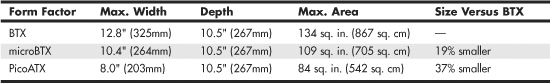
BTX includes three definitions of motherboard size, as shown in Table 4.1.
Table 4.1 BTX Motherboard Form Factors
Each board has the same basic screw hole and connector placement requirements. So, if you have a case that fits a full-size BTX board, you can also mount a microBTX or picoBTX board in that same case (see Figure 4.10). Obviously, if you have a smaller case designed for MicroBTX or picoBTX, you won’t be able to put the larger microBTX or BTX boards in that case.
Figure 4.10 BTX specification 1.0a motherboard dimensions.

BTX requires up to 10 mounting holes and supports up to seven slots, depending on the size, as shown in Table 4.2.
Table 4.2 BTX Motherboard Mounting Holes

BTX also clearly specifies volumetric zones around the motherboard to prevent any interference from the chassis or internal components such as drives, which allows for maximum interchangeability without physical interference or fit problems.
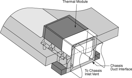
With processors exceeding 100W in thermal output, as well as voltage regulators, motherboard chipsets, and video cards adding to the thermal load in a system, BTX was designed to allow all the high-heat-producing core components to be mounted inline from front to back, so that a single high-efficiency thermal module (heatsink) can cool the system. This eliminates the need for an excessive number of fans. The thermal module includes a heatsink for the processor, a high-efficiency fan, and a duct to direct airflow through the system. Extra support for the thermal module is provided under the board via a support and retention module (SRM), which provides structural support for heatsinks that are much heavier than allowed in ATX designs (see Figure 4.11).
Figure 4.11 BTX thermal module containing a processor heatsink and fan.
BTX uses the same power connectors as in the latest power supply form factor specifications, including a 24-pin main connector for the board and a 4-pin ATX12V connector for the CPU voltage regulator module. The particular power supply form factor used depends mostly on the chassis selected.
A typical tower system has components arranged as shown in Figure 4.12.
Figure 4.12 BTX tower chassis layout.
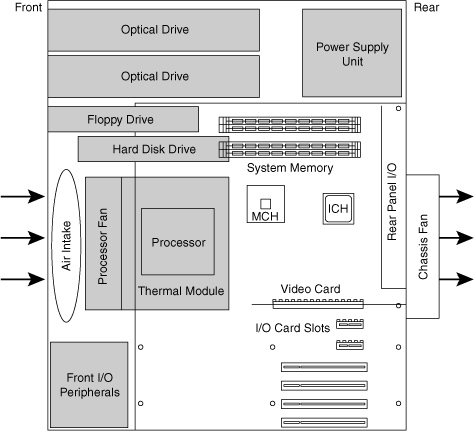
From Figure 4.12, you can see that the main heat-producing core components are centrally located inline from front to rear, allowing the most efficient thermal design. Air flows from front to rear through the center, cooling the processor, motherboard chipset, memory, and video card.
To support the heavy processor heatsink and thermal module assembly, an SRM is mounted under the board. The SRM is essentially a metal plate affixed to the chassis under the board, and the thermal module is bolted directly to the SRM instead of to the motherboard. This helps carry the weight of the module and prevents excessive loads from being applied to the processor and motherboard, especially during the shipping and handling of the system.
The BTX I/O connector area is similar to ATX, except that it is at the opposite side of the rear of the board. The size of the area is slightly shorter but wider than ATX, allowing a large number of interfaces and connectors to be built into the motherboard.
Systems using BTX were produced primarily from 2005 through 2007 by companies such as Dell, Gateway, and others. After that, a lack of new BTX motherboards and cases forced most system manufacturers and builders to revert back to the more popular ATX-based form factors. Other large manufacturers such as HP never jumped on the BTX bandwagon, instead staying with ATX-based systems. Because of the lack of BTX component popularity and other problems, I recommend avoiding BTX systems and components such as motherboards and chassis because they will be difficult to upgrade or replace in the future. ATX remains by far the most popular and recommended form factor for system builders and upgraders.
ATX and Other Modern Form Factors
The following sections cover the industry-standard form factors, including ATX, that are popular on modern systems.
ATX
The ATX form factor was the first of a dramatic evolution in motherboard form factors. ATX is a combination of the best features of the Baby-AT and LPX motherboard designs, with many new enhancements and features thrown in. The ATX form factor is essentially a Baby-AT motherboard turned sideways in the chassis, along with a modified power supply location and connector. The most important thing to know initially about the ATX form factor is that it is physically incompatible with either the previous Baby-AT or LPX design. In other words, a different case and power supply are required to match the ATX motherboard. These case and power supply designs have become common and are found in most new systems.
Intel initially released the official ATX specification in July 1995. It was written as an open specification for the industry. ATX boards didn’t hit the market in force until mid-1996, when they rapidly began replacing Baby-AT boards in new systems. The ATX specification was updated to version 2.01 in February 1997, 2.03 in May 2000, 2.1 in June 2002, and 2.2 in February 2004. Intel publishes these detailed specifications so other manufacturers can use the interchangeable ATX design in their systems. The current specifications for ATX and other current motherboard types are available online from the Desktop Form Factors site: www.formfactors.org. ATX is the most popular motherboard form factor for new systems through 2007 and will continue to be popular in the future. An ATX system will be upgradeable for many years to come, exactly like Baby-AT was in the past.
ATX improved on the Baby-AT and LPX motherboard designs in several major areas:
• Built-in double high external I/O connector panel—The rear portion of the motherboard includes a stacked I/O connector area that is 6 1/4″ wide by 1 3/4″ tall. This enables external I/O connectors to be located directly on the board and minimizes the need for cables running from internal connectors to the back of the case as with Baby-AT designs.
• Single main keyed internal power supply connector—The ATX specification includes a keyed and shrouded main power connector that is easy to plug in and which can’t easily be installed incorrectly. This connector also features pins for supplying 3.3V to the motherboard, helping to minimize the use of built-in voltage regulators that are susceptible to failure.
![]() See “Motherboard Power Connectors,” p. 937 (Chapter 18, “Power Supplies”).
See “Motherboard Power Connectors,” p. 937 (Chapter 18, “Power Supplies”).
• Relocated CPU and memory—The CPU and memory modules are relocated so they can’t interfere with any bus expansion cards and can easily be accessed for upgrade without removing any of the installed bus adapters.
• Relocated internal I/O connectors—The internal I/O connectors for the floppy and hard disk drives are relocated to be near the drive bays and out from under the expansion board slot and drive bay areas.
• Improved cooling—The CPU and main memory are designed and positioned to improve overall system cooling.
• Lower cost to manufacture—The ATX specification eliminates the need for the rat’s nest of cables to external I/O port connectors found on Baby-AT motherboards.
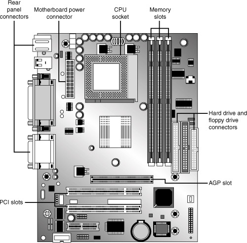
Figure 4.13 shows the typical ATX system layout and chassis features, as you would see them looking in with the lid off on a desktop, or sideways in a tower with the side panel removed. Notice how virtually the entire motherboard is clear of the drive bays and how the devices such as CPU, memory, and internal drive connectors are easy to access and do not interfere with the bus slots.
Figure 4.13 Typical ATX system layout.

Note
Although most ATX systems mount the power supply near the processor (on top in most tower arrangements), this is not a requirement of the standard. Some systems mount the power supply in other locations (such as on the bottom).
The ATX motherboard shape is basically a Baby-AT design rotated sideways 90°. The expansion slots are now parallel to the shorter side dimension and do not interfere with the CPU, memory, or I/O connector sockets (see Figure 4.14). In addition to a full-size ATX layout, Intel originally specified a Mini-ATX design, which is a fully compatible subset of ATX that fits into the same case:
• A full-size ATX board is 12″ wide × 9.6″ deep (305mm×244mm).
• The Mini-ATX board is 11.2″×8.2″ (284mm×208mm).
Figure 4.14 ATX specification 2.2 motherboard dimensions. Most recent ATX motherboards no longer use ISA expansion slots.

Mini-ATX is not an official standard; instead it is simply referenced as a slightly smaller version of ATX. In fact, all references to Mini-ATX were removed from the ATX 2.1 and later specifications. Two smaller official versions of ATX exist, called microATX and FlexATX. They are discussed in the following sections.
Although the case holes are similar to the Baby-AT case, cases for Baby-AT and ATX are generally incompatible. The ATX power supply design is identical in physical size to the standard Slimline power supply used with Baby-AT systems; however, they also use different connectors and supply different voltages.
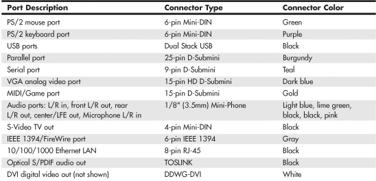
The best way to tell whether your system has an ATX-family motherboard design without removing the lid is to look at the back of the system. Two distinguishing features identify ATX. One is that the expansion boards plug directly into the motherboard. There is usually no riser card as with LPX and NLX (except for certain Slimline systems, such as rack-mounted servers), so the slots are usually perpendicular to the plane of the motherboard. Also, ATX boards have a unique double-high connector area for all the built-in connectors on the motherboard (see Figure 4.15 and Table 4.3). This is found just to the side of the bus slot area and can be used to easily identify an ATX board.
Figure 4.15 ATX motherboard and rear panel connections from systems with onboard sound and video (top and middle), networking and IEEE 1394/FireWire (middle and bottom), and a “legacy-free” system (bottom).

Table 4.3 Built-in Ports Usually Found on ATX Motherboards

Note
Most ATX motherboards feature connectors with industry-standardized color codes (shown in the previous table). This makes plugging in devices much easier and more foolproof: You merely match up the colors. For example, most keyboards have a cable with a purple plug, whereas most mice have a cable with a green plug. Even though the keyboard and mouse connectors on the motherboard appear the same (both are 6-pin Mini-DIN types), their color-coding matches the plugs on the respective devices. Therefore, to plug them in properly, you merely insert the purple plug into the purple connector and the green plug into the green connector. This saves you from having to bend down to try to decipher small labels on the connectors to ensure you get them right.
The specifications and related information covering the ATX and related form factors are available from the Form Factors website at www.formfactors.org. The Form Factors site provides form factor specifications and design guides, as well as design considerations for new technologies, information on initiative supporters, vendor products, and a form factor discussion forum.
Note
Some motherboards, especially those used in server systems, come in nonstandard ATX variations collectively called extended ATX. This is a term applied to boards that are compatible with ATX but that are deeper. Standard ATX is 12″×9.6″ (305mm×244mm), whereas extended ATX boards are up to 12″×13″ (305mm×330mm). Because technically no official “extended ATX” standard exists, compatibility problems can exist with boards and chassis claiming to support extended ATX. When purchasing an extended ATX board, be sure it will fit in the chassis you intend to use. Dual Xeon processors fit in a standard ATX-size board, so choose a standard ATX-size board for maximum compatibility with the existing ATX chassis.
microATX
microATX is a motherboard form factor Intel originally introduced in December 1997, as an evolution of the ATX form factor for smaller and lower-cost systems. The reduced size as compared to standard ATX allows for a smaller chassis, motherboard, and power supply, thereby reducing the cost of the entire system. The microATX form factor is also backward-compatible with the ATX form factor and can be used in full-size ATX cases. Of course, a microATX case doesn’t take a full-size ATX board. This form factor has become popular in the low-cost PC market. Currently, mini-tower chassis systems dominate the low-cost PC market, although their small sizes and cramped interiors severely limit future upgradeability.
The main differences between microATX and standard or Mini-ATX are as follows:
• Reduced width motherboard (9.6″ [244mm] instead of 12″ [305mm] or 11.2″ [284mm])
• Fewer I/O bus expansion slots (four maximum, although most boards feature only three)
• Smaller power supply optional (SFX/TFX form factors)
The microATX motherboard maximum size is only 9.6″×9.6″ (244mm×244mm) as compared to the full-size ATX size of 12″×9.6″ (305mm×244mm) or the Mini-ATX size of 11.2″×8.2″ (284mm×208mm). Even smaller boards can be designed as long as they conform to the location of the mounting holes, connector positions, and so on, as defined by the standard. Fewer slots aren’t a problem for typical home or small-business PC users because more components such as sound and video are usually integrated on the motherboard and therefore don’t require separate slots. This higher integration reduces motherboard and system costs. External buses, such as USB, 10/100/1000 Ethernet, and optionally 1394 (FireWire), can provide additional expansion out of the box. The specifications for microATX motherboard dimensions are shown in Figure 4.16.
Figure 4.16 microATX specification 1.2 motherboard dimensions.
Smaller form factor (called SFX or TFX) power supplies have been defined for optional use with microATX systems, although the standard ATX supply also works fine because the connectors are the same. The smaller size SFX/TFX power supplies encourage flexibility in choosing mounting locations within the chassis and allow for smaller systems that consume less power overall. Although the smaller supplies can be used, they may lack sufficient power output for faster or more fully configured systems. Because of the high power demands of most modern systems, most third-party microATX chassis are designed to accept standard ATX power supplies, although microATX systems sold by vendors such as Compaq, HP, and eMachines typically use some type of SFX or TFX power supply to reduce costs.
![]() See “Power Supply Form Factors,” p. 917 (Chapter 18).
See “Power Supply Form Factors,” p. 917 (Chapter 18).
The microATX form factor is similar to ATX for compatibility. The similarities include the following:
• Standard ATX power connectors.
• Standard ATX I/O panel.
• Mounting holes and dimensions are a subset of ATX.
These similarities ensure that a microATX motherboard can easily work in a standard ATX chassis with a standard ATX power supply, as well as the smaller microATX chassis and SFX/TFX power supply.
The overall system size for a microATX is very small. A typical case is only 12″–14″ tall, about 7″ wide, and 12″ deep. This results in a kind of micro-tower or desktop size. A typical microATX motherboard is shown in Figure 4.17.
Figure 4.17 A typical microATX motherboard’s dimensions are 9.6″×9.6″.
As with ATX, Intel released microATX to the public domain to facilitate adoption as a de facto standard. The specification and related information on microATX are available through the Desktop Form Factors site (www.formfactors.org).
FlexATX
In March 1999, Intel released the FlexATX addendum to the microATX specification. This added a new and even smaller variation of the ATX form factor to the motherboard scene. FlexATX’s smaller design is intended to allow a variety of new PC designs, especially extremely inexpensive, smaller, consumer-oriented, appliance-type systems. Some of these designs might not even have expansion slots, allowing expansion only through USB or IEEE 1394/FireWire ports.
FlexATX defines a board that is up to 9″×7.5″ (229mm×191mm) in size, which is the smallest of the ATX family boards. In all other ways, FlexATX is the same as ATX and microATX, making FlexATX fully backward compatible with ATX or microATX by using a subset of the mounting holes and the same I/O and power supply connector specifications (see Figure 4.18).
Figure 4.18 Size and mounting hole comparison between ATX, microATX, and FlexATX motherboards.

Most FlexATX systems likely use SFX/TFX (small or thin form factor) type power supplies (introduced in the microATX specification), although if the chassis allows it, a standard ATX power supply can also be used.
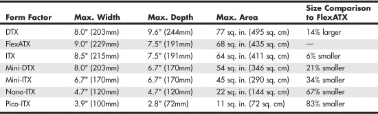
The addition of FlexATX gave the family of ATX boards four definitions of size (three are the official standards), as shown in Table 4.4.
Table 4.4 ATX Motherboard Form Factors

Note that these dimensions are the maximums allowed. Making a board smaller in any given dimension is always possible as long as it conforms to the mounting hole and connector placement requirements detailed in the respective specifications. Each board has the same basic screw hole and connector placement requirements, so if you have a case that fits a full-size ATX board, you could also mount a microATX or FlexATX board in that same case. Obviously, if you have a smaller case designed for microATX or FlexATX, you won’t be able to put the larger Mini-ATX or full-size ATX boards in that case.
DTX and Mini-DTX
The DTX (and Mini-DTX) specification was released in February 2007 by AMD, and is available for download from www.dtxpc.org. DTX and Mini-DTX are smaller variations of the microATX and FlexATX specifications, respectively. DTX boards are up to 8″×9.6″ in size, whereas Mini-DTX boards are a shorter version at only 8″×6.7″ in size. Mini-DTX boards incorporate only four mounting holes (C, F, H, and J), whereas DTX boards add two more for a total of six (C, F, H, J, L, and M). Refer to Figure 4.19 for the respective hole locations. The size of the DTX and Mini-DTX boards as they relate to FlexATX are shown in Table 4.5. The narrow 8″ width for both DTX and Mini-DTX boards allows for only two expansion slots.
Figure 4.19 Top and rear views of the VIA EPIA-V motherboard, a typical Mini-ITX motherboard. Photo courtesy VIA Technologies, Inc.

Table 4.5 Comparing the FlexATX, ITX, and Mini-ITX Form Factors
ITX and Mini-ITX
FlexATX defines a board that is up to 9″×7.5″ in size. Note the up to part of the dimensions, which means that, even though those dimensions are the maximums, less is also allowed. Therefore, a FlexATX board can be smaller than that, but how much smaller? By analyzing the FlexATX specification—and, in particular, studying the required mounting screw locations—you can see that a FlexATX board could be made small enough to use only four mounting holes (C, F, H, and J). Refer to Figure 4.16 for the respective hole locations.
According to the FlexATX standard, the distance between holes H and J is 6.2″, and the distance between hole J and the right edge of the board is 0.25″. By leaving the same margin from hole H to the left edge, you could make a board with a minimum width of 6.7″ (0.25″ + 6.2″ + 0.25″) that would conform to the FlexATX specification. Similarly, the distance between holes C and H is 6.1″, and the distance between hole C and the back edge of the board is 0.4″. By leaving a minimum 0.2″ margin from hole H to the front edge, you could make a board with a minimum depth of 6.7″ (0.4″ + 6.1″ + 0.2″) that would conform to the FlexATX specification. By combining the minimum width and depth, you can see that the minimum board size that would conform to the FlexATX specification is 6.7″×6.7″ (170mm×170mm).
VIA Technologies Platform Solutions Division wanted to create a motherboard as small as possible, yet not define a completely new and incompatible form factor. To accomplish this, in March 2001 VIA created a board that was slightly narrower in width (8.5″ instead of 9″) but still the same depth as FlexATX, resulting in a board that was 6% smaller and yet still conformed to the FlexATX specification. VIA called this ITX but then realized that the size savings were simply too small to justify developing it further, so it was discontinued before any products were released.
In April 2002, VIA created an even smaller board that featured the absolute minimum width and depth dimensions allowed by FlexATX. The company called it Mini-ITX. In essence, all Mini-ITX boards are simply FlexATX boards that are limited to the minimum allowable dimensions. All other aspects, including the I/O aperture size and location, screw hole locations, and power supply connections, are pure FlexATX. A Mini-ITX board fits in any chassis that accepts a FlexATX board; however, larger boards will not fit into a Mini-ITX chassis.
The Mini-ITX form factor was designed by VIA especially to support VIA’s low-power embedded Eden ESP and C3 E-Series processors. Only a very small number of motherboards is available in this form factor, and only from VIA and one or two other manufacturers. Because the processors used on these boards are substantially less powerful than even the old Intel Celeron 4 and AMD Duron entry-level processors, the Mini-ITX form factor is intended for use mainly in nontraditional settings such as set-top boxes and computing appliances. The size of the ITX and Mini-ITX boards as they relate to FlexATX is shown in Table 4.5.
Whereas the still-born ITX format was virtually the same as FlexATX in size (which is probably why it was discontinued before any were sold), Mini-ITX motherboards are 170mm×170mm (6.7″×6.7″), which is 34% smaller than the maximum allowed by FlexATX.
To take advantage of the smaller Mini-ITX format, several chassis makers have produced very small chassis to fit these boards. Most are the shape of a small cube, with one floppy and one optical drive bay visible from the front. The layout of a typical Mini-ITX motherboard, the VIA EPIA-V, is shown in Figure 4.19.
Mini-ITX motherboards can offer a full range of input-output ports. However, several differences exist between the Mini-ITX motherboards and other ATX designs:
• The processor on a Mini-ITX motherboard is usually permanently soldered to the board, making future processor upgrades or replacements impossible.
• Most Mini-ITX chassis use TFX power supplies, for which there are currently only a few suppliers. Consequently, replacements for them are more expensive and more difficult to find.
• The available TFX power supplies are rated for less output than larger supplies, typically up to 240 watts maximum.
• There is no provision for replacing onboard video with an AGP video card.
Because Mini-ITX boards and chassis are made by only a small number of suppliers, future upgrades or parts replacements are limited. However, Mini-ITX boards are actually considered FlexATX boards as well, so they can be installed in any standard FlexATX, microATX, or full-size ATX chassis and use the corresponding power supplies. The only caveats are that the smaller Mini-ITX chassis will not accept larger FlexATX, microATX, or full-size ATX boards and most Mini-ITX chassis accept only TFX power supplies. When you select a Mini-ITX system, you must be sure to select the appropriate processor type and speed necessary for the task you need it to perform because processor replacements or upgrades almost always require changing the entire motherboard.
Note
The official site for ITX information is www.viaembedded.com. The site www.mini-itx.com is often mistaken for an official site, but it is actually a vendor that specializes in ITX systems and component sales.
The latest developments in the ITX family are the Nano-ITX and Pico-ITX form factors, ultra-compact (120mm×120mm and 100mm×72mm) platforms that are designed for extreme low-power embedded applications.
Proprietary Designs
Motherboards that are not one of the industry standard form factors, such as any of the ATX formats, are deemed proprietary or semiproprietary. Most people purchasing PCs should avoid proprietary designs because they do not allow for a future motherboard, power supply, or case upgrade, which limits future use and serviceability of the system. To me, proprietary systems are disposable PCs because you can neither upgrade them nor easily repair them. The problem is that the proprietary parts often come only from the original system manufacturer, and they usually cost much more than industry standard parts. Therefore, after your proprietary system goes out of warranty, it is essentially no longer worth upgrading or repairing. If the motherboard or any component on it goes bad, you will be better off purchasing a completely new standard system than paying many times the normal price for a new proprietary motherboard. In addition, a new industry standard motherboard would be newer and faster than the one you would be replacing. In a proprietary system, the replacement board would not only cost way too much, but it would be the same as the one that failed.
Processor Sockets/Slots
The CPU is installed in either a socket or a slot, depending on the type of chip.
Starting with the 486 processors, Intel designed the processor to be a user-installable and replaceable part and developed standards for CPU sockets and slots that would allow different models of the same basic processor to plug in. One key innovation was to use a zero insertion force (ZIF) socket design, which meant that the processor could be easily installed or removed with no tools. ZIF sockets use a lever to engage or release the grip on the chip, and with the lever released, the chip can be easily inserted or removed. The ZIF sockets were given a designation that was usually imprinted or embossed on the socket indicating what type it was. Different socket types accepted different families of processors. If you know the type of socket or slot on your motherboard, you essentially know which types of processors are designed to plug in.
![]() See “Processor Socket and Slot Types,” p. 86 (Chapter 3, “Processor Types and Specifications”).
See “Processor Socket and Slot Types,” p. 86 (Chapter 3, “Processor Types and Specifications”).
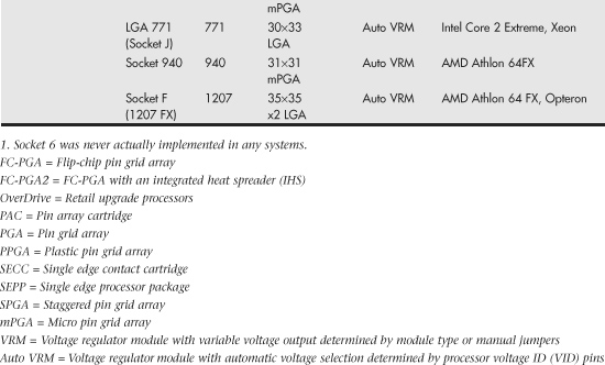
Table 4.6 shows the designations for the various industry-standard processor sockets/slots and lists the chips designed to plug into them.
Table 4.6 CPU Socket Specifications


Originally, all processors were mounted in sockets (or soldered directly to the motherboard). Whereas most processors plug into sockets, both Intel and AMD temporarily shifted to a slot-based approach for their processors in the late 1990s because the processors began incorporating built-in L2 cache, purchased as separate chips from third-party Static RAM (SRAM) memory chip manufacturers. Therefore, the processor then consisted not of one but of several chips, all mounted on a daughterboard that was then plugged into a slot in the motherboard. This worked well, but there were additional expenses in the extra cache chips, the daughterboard itself, the slot, optional casings or packaging, and the support mechanisms and physical stands and latches for the processor and heatsink. All in all, slot-based processors were expensive to produce compared to the previous socketed versions.
With the advent of the second-generation Celeron, Intel began integrating the L2 cache directly into the processor die, meaning no extra chips were required. The second-generation (code-named Coppermine) Pentium III also received on-die L2 cache, as did the second-generation Athlon (code-named Thunderbird) processor from AMD. With on-die L2 cache, the processor was back to being a single chip again, which also meant that mounting it on a separate board plugged into a slot was unnecessary. All modern processors now have integrated L2 cache (some also have integrated L3 cache) and use the socket form. As a bonus, on-die cache runs at full processor speed, instead of the one-half or one-third speed of the cache in slot-based processors.
Chipsets
We can’t talk about modern motherboards without discussing chipsets. The chipset is the motherboard; therefore, any two boards with the same chipsets will offer essentially the same level of performance and features.
Depending on the model, the chipset usually contains the processor bus interface (called front-side bus, or FSB), memory controllers, bus controllers, I/O controllers, and more. All the primary circuits of the motherboard are contained within the chipset. If the processor in your PC is like the engine in your car, the chipset represents the drivetrain and chassis. It is the framework in which the engine rests and is its connection to the outside world. The chipset is the frame, suspension, steering, wheels and tires, transmission, drive shaft, differential, and brakes. The chassis in your car is what gets the power to the ground, allowing the vehicle to start, stop, and corner. In the PC, the chipset represents the connection between the processor and everything else. The processor can’t talk to the adapter boards, devices, memory (in some models), and so on without going through the chipset. If you think of the processor as the brain, the chipset is the spine and central nervous system.
Because the chipset controls the interface or connections between the processor and just about everything else, the chipset ends up dictating which type of processor you have; how fast the buses will run; and in some cases the speed, type, and amount of memory you can use. In fact, the chipset might be the single most important component in your system, possibly even more important than the processor. I’ve seen systems with a faster processor be outperformed by systems with a slower processor but a better chipset, much like how a car with less power might win a race through better cornering and braking. When deciding on a system, I start by choosing the chipset because the chipset decision dictates the processor, I/O, and expansion capabilities.
Chipset Evolution
When IBM created the first PC motherboards, it used several discrete (separate) chips to complete the design. Besides the processor and optional math coprocessor, many other components were required to complete the system. These other components included items such as the clock generator, bus controller, system timer, interrupt and DMA controllers, CMOS RAM and clock, and keyboard controller. Additionally, many other simple logic chips were used to complete the entire motherboard circuit, plus, of course, things such as the actual processor, math coprocessor (floating-point unit), memory, and other parts. Table 4.7 lists all the primary chip components used on the original PC/XT and AT motherboards.
Table 4.7 Primary Chip Components on PC/XT and AT Motherboards

In addition to the processor/coprocessor, a six-chip set was used to implement the primary motherboard circuit in the original PC and XT systems. IBM later upgraded this to a nine-chip design in the AT and later systems, mainly by adding more interrupt and DMA controller chips and the nonvolatile CMOS RAM/real-time clock chip. All these motherboard chip components came from Intel or an Intel-licensed manufacturer, except the CMOS/clock chip, which came from Motorola. To build a clone or copy of one of these IBM systems required all these chips plus many smaller discrete logic chips to glue the design together, totaling 100 or more individual chips. This kept the price of a motherboard high and left little room on the board to integrate other functions.
In 1986, a company called Chips and Technologies introduced a revolutionary component called the 82C206—the main part of the first PC motherboard chipset. This was a single chip that integrated into it all the functions of the main motherboard chips in an AT-compatible system. This chip included the functions of the 82284 clock generator, 82288 bus controller, 8254 system timer, dual 8259 interrupt controllers, dual 8237 DMA controllers, and even the MC146818 CMOS/clock chip. Besides the processor, virtually all the major chip components on a PC motherboard could now be replaced by a single chip. Four other chips augmented the 82C206 acting as buffers and memory controllers, thus completing virtually the entire motherboard circuit with five total chips. This first chipset was called the CS8220 chipset by Chips and Technologies. Needless to say, this was a revolutionary concept in PC motherboard manufacturing. Not only did it greatly reduce the cost of building a PC motherboard, but it also made designing a motherboard much easier. The reduced component count meant the boards had more room for integrating other items formerly found on expansion cards. Later, the four chips augmenting the 82C206 were replaced by a new set of only three chips, and the entire set was called the New Enhanced AT (NEAT) CS8221 chipset. This was later followed by the 82C836 Single Chip AT (SCAT) chipset, which finally condensed all the chips in the set down to a single chip.
The chipset idea was rapidly copied by other chip manufacturers. Companies such as Acer, Erso, Opti, Suntac, Symphony, UMC, and VLSI each gained an important share of this market. Unfortunately for many of them, the chipset market has been a volatile one, and many of them have long since gone out of business. In 1993, VLSI had become the dominant force in the chipset market and had the vast majority of the market share; by the next year, VLSI (which later was merged into Philips Semiconductors), along with virtually everybody else in the chipset market, was fighting to stay alive. This is because a new chipset manufacturer had come on the scene, and within a year or so of getting serious, it was totally dominating the chipset market. That company was Intel, and after 1994, it had a virtual lock on the chipset market. If you have a motherboard built since 1994 that uses or accepts an Intel processor, chances are good that it has an Intel chipset on it as well.
Today, Intel is not alone in the chipset business: ATI (now part of AMD), NVIDIA, VIA Technologies, and Silicon Integrated Systems (SiS) all make or have made chipsets for Intel-based systems as well.
Although AMD (and ATI which is now a part of AMD) has developed its own chipsets, NVIDIA and SIS also produce chipsets for AMD-based systems.
It is interesting to note that the original PC chipset maker, Chips and Technologies, survived by changing course to design and manufacture video chips and found a niche in that market specifically for laptop and notebook video chipsets. Chips and Technologies was subsequently purchased by Intel in 1998 as a part of Intel’s video strategy.
Intel Chipsets
You can’t talk about chipsets today without discussing Intel because it currently owns the vast majority of the chipset market. It is interesting to note that we probably have Compaq to thank for forcing Intel into the chipset business in the first place!
The thing that really started it all was the introduction of the EISA bus designed by Compaq in 1989. At that time, Compaq had shared the bus with other manufacturers in an attempt to make it a market standard. However, Compaq refused to share its EISA bus chipset—a set of custom chips necessary to implement this bus on a motherboard.
Enter Intel, who decided to fill the chipset void for the rest of the PC manufacturers wanting to build EISA bus motherboards. As is well known today, the EISA bus failed to become a market success, except for a short-term niche server business, but Intel now had a taste of the chipset business—and this it apparently wouldn’t forget. With the introduction of the 286 and 386 processors, Intel became impatient with how long it took the other chipset companies to create chipsets around its new processor designs; this delayed the introduction of motherboards that supported the new processors. For example, it took more than 2 years after the 286 processor was introduced for the first 286 motherboards to appear and just over a year for the first 386 motherboards to appear after the 386 had been introduced. Intel couldn’t sell its processors in volume until other manufacturers made motherboards that would support them, so it thought that by developing motherboard chipsets for a new processor in parallel with the new processor, it could jumpstart the motherboard business by providing ready-made chipsets for the motherboard manufacturers to use.
Intel tested this by introducing the 420 series chipsets along with its 486 processor in April 1989. This enabled the motherboard companies to get busy right away, and in only a few months the first 486 motherboards appeared. Of course, the other chipset manufacturers weren’t happy; now they had Intel as a competitor, and Intel would always have chipsets for new processors on the market first!
Intel then realized that it made both processors and chipsets, which were 90% of the components on a typical motherboard. What better way to ensure that motherboards were available for its Pentium processor when it was introduced than by making its own motherboards as well and having these boards ready on the new processor’s introduction date. When the first Pentium processor debuted in 1993, Intel also debuted the 430LX chipset as well as a fully finished motherboard. Now, besides the chipset companies being upset, the motherboard companies weren’t too happy, either. Intel was not only the major supplier of parts needed to build finished boards (processors and chipsets), but was now building and selling the finished boards as well. By 1994, Intel dominated the processor and chipset markets and had cornered the motherboard market as well.
Now as Intel develops new processors, it develops chipsets and motherboards simultaneously, which means they can be announced and shipped in unison. This eliminates the delay between introducing new processors and waiting for motherboards and systems capable of using them, which was common in the industry’s early days. For the consumer, this means no waiting for new systems. Since the original Pentium processor in 1993, we have been able to purchase ready-made systems on the same day a new processor is released.
Intel Chipset Model Numbers
Starting with the 486 in 1989, Intel began a pattern of numbering its chipsets as shown in Table 4.8.
Table 4.8 Intel Chipset Model Numbers

The chipset numbers listed here are abbreviations of the actual chipset numbers stamped on the individual chips. For example, one of the popular Pentium II/III chipsets was the Intel 440BX chipset, which consisted of two components: the 82443BX North Bridge and the 82371EB South Bridge. Likewise, the 865G chipset supports the Pentium 4 and consists of two main parts: the 82865G graphics memory controller hub (GMCH; replaces the North Bridge and includes integrated video) and an 82801EB or 82801EBR I/O controller hub (ICH5 or ICH5R; replaces the South Bridge). Finally, the X58 chipset supports Socket LGA1366 versions of the Core i Series processors, and normally consists of the 82X58 IOH (I/O Hub) and either an 82801JIB or 82801JIR I/O controller hub (ICH10 or ICH10R). By reading the logo (Intel or others) as well as the part number and letter combinations on the larger chips on your motherboard, you can identify the chipset your motherboard uses.
Intel has used two distinct chipset architectures: a North/South Bridge architecture and a newer hub architecture. All chipsets introduced from the 800 series on use the hub architecture.
Tip
In many cases, the North Bridge/GMCH/MCH/IOH chip on recent motherboards is covered up with a passive or active heatsink, and some motherboards also use a heatsink on the South Bridge or ICH chip. To determine the chipset used in these systems, I recommend software such as the Intel Chipset Identification Utility (http://developer.intel.com/support/chipsets/inf/sb/CS-009266.htm) or CPU-Z (http://cpuid.com).
Intel Integrated Graphics Architecture
Intel began producing motherboard chipsets with integrated video starting with the 810 chipset in April 1999. By building the graphics directly into the motherboard chipset, no other graphics chip or video memory was required, meaning that video could be essentially included in a PC for “free.” Many of the chipsets including integrated graphics also support either AGP or PCI Express video slots for upgrades, meaning that the integrated graphics could easily be upgraded by adding a discrete graphics card.
See Table 12.2 in Chapter 12, “Video Hardware,” for the types and features for the integrated graphics available in Intel motherboard chipsets over the years.
While not designed to challenge discrete graphics chips on dedicated graphics cards, integrated video can offer reasonable graphics performance for virtually no cost. I often recommend using motherboards that feature integrated graphics as well as a slot for adding a video card later; that way you can start off by saving money using the integrated graphics, and later upgrade to a higher performance video solution by merely adding a card.
![]() See “Integrated Video/Motherboard Chipsets,” p. 673 (Chapter 12).
See “Integrated Video/Motherboard Chipsets,” p. 673 (Chapter 12).
AMD Chipsets
AMD took a gamble with its Athlon family of processors. With these processors, AMD decided for the first time to create a chip that was Intel compatible with regard to software but not directly hardware or pin compatible. Whereas the K6 series would plug into the same Socket 7 that Intel designed for the Pentium processor line, the AMD Athlon and Duron would not be pin compatible with the Pentium II/III and Celeron chips. This also meant that AMD could not take advantage of the previously existing chipsets and motherboards when the Athlon and Duron were introduced; instead, AMD would have to either create its own chipsets and motherboards or find other companies who would.
The gamble has paid off. AMD bootstrapped the market by introducing its own chipset, referred to as the AMD-750 chipset (code-named Irongate). The AMD 750 chipset consists of the 751 system controller (North Bridge) and the 756 peripheral bus controller (South Bridge). AMD followed with the AMD-760 chipset for the Athlon/Duron processors, which was the first major chipset on the market supporting DDR SDRAM for memory. It consists of two chips—the AMD-761 system bus controller (North Bridge) and the AMD-766 peripheral bus controller (South Bridge). Similarly, AMD established a new standard chipset architecture for its line of 64-bit processors—the Athlon 64 and Opteron—by developing the AMD-8000 chipset. AMD’s pioneering efforts have inspired other companies, such as VIA Technologies, NVIDIA, SiS, and ATI to develop chipsets specifically designed to interface with AMD processors. In 2007, AMD purchased ATI, essentially bringing both motherboard chipsets and video processors in-house. This puts AMD on a level more equal to Intel because it gives the company the capability to produce most of the chips necessary to build a system around its processors. Since then AMD and NVIDIA have produced the majority of chipsets for AMD-based systems.
Traditional North/South Bridge Architecture
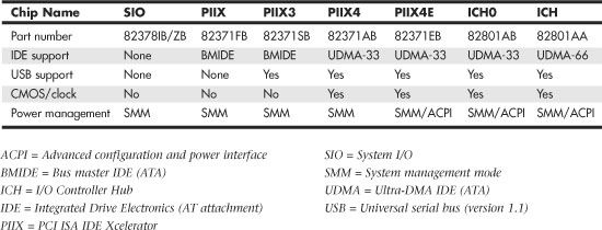
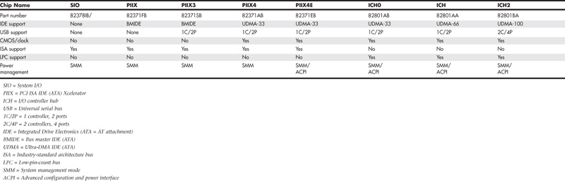
Most of Intel’s earlier chipsets (and, until a few years ago, virtually all non-Intel chipsets) are broken into a multitiered architecture incorporating what are referred to as North and South Bridge components, as well as a Super I/O chip:
• The North Bridge—So named because it is the connection between the high-speed processor bus and the slower AGP and PCI buses. The North Bridge is what the chipset is named after, meaning that, for example, what we call the 440BX chipset is derived from the fact that the actual North Bridge chip part number for that set is 82443BX.
• The South Bridge—So named because it is the bridge between the PCI bus (66/33MHz) and the even slower ISA bus (8MHz).
• The Super I/O chip—It’s a separate chip attached to the ISA bus that is not really considered part of the chipset and often comes from a third party, such as National Semiconductor or Standard MicroSystems Corp. (SMSC). The Super I/O chip contains commonly used peripheral items all combined into a single chip. Note that most recent South Bridge chips now include Super I/O functions (such chips are known as Super-South Bridge chips), so that most recent motherboards no longer include a separate Super I/O chip.
![]() See “Super I/O Chips,” p. 258 (this chapter).
See “Super I/O Chips,” p. 258 (this chapter).
Figure 4.20 shows a typical AMD Socket A motherboard using North/South Bridge architecture with the locations of all chips and components.
Figure 4.20 A typical Socket A (AMD Athlon/Duron) motherboard showing component locations.

The North Bridge is sometimes referred to as the PAC (PCI/AGP Controller). It is essentially the main component of the motherboard and is the only motherboard circuit besides the processor that normally runs at full motherboard (processor bus) speed. Most modern chipsets use a single-chip North Bridge; however, some of the older ones actually consisted of up to three individual chips to make up the complete North Bridge circuit.
The South Bridge is the lower-speed component in the chipset and has always been a single individual chip. The South Bridge is a somewhat interchangeable component in that different chipsets (North Bridge chips) often are designed to use the same South Bridge component. This modular design of the chipset allows for lower cost and greater flexibility for motherboard manufacturers. Similarly, many vendors produce several versions of pin-compatible South Bridge chips with different features to enable more flexible and lower-cost manufacturing and design. The South Bridge connects to the 33MHz PCI bus and contains the interface or bridge to the 8MHz ISA bus (if present). It also typically contains dual ATA/IDE hard disk controller interfaces, one or more USB interfaces, and in later designs even the CMOS RAM and real-time clock functions. In older designs, the South Bridge contained all the components that make up the ISA bus, including the interrupt and DMA controllers. The third motherboard component, the Super I/O chip, is connected to the 8MHz ISA bus or the low pin count (LPC) bus and contains all the standard peripherals that are built into a motherboard. For example, most Super I/O chips contain the serial ports, parallel port, floppy controller, and keyboard/mouse interface. Optionally, they might contain the CMOS RAM/clock, IDE controllers, and game port interface as well. Systems that integrate IEEE 1394 and SCSI ports use separate chips for these port types.
Most recent motherboards that use North/South Bridge chipset designs incorporate a Super-South Bridge, which incorporates the South Bridge and Super I/O functions into a single chip.
Hub Architecture
Beginning in 1999, chipsets from Intel began using hub architectures in which the former North Bridge chip is now called a Memory Controller Hub (MCH) or an I/O Hub (IOH) and the former South Bridge is called an I/O Controller Hub (ICH). Systems that include integrated graphics use a Graphics Memory Controller Hub (GMCH) in place of the standard MCH. Rather than being connected through the PCI bus as in a standard North/South Bridge design, they are connected via a dedicated hub interface that is at least twice as fast as PCI. The hub design offers several advantages over the conventional North/South Bridge design:
• It’s faster—The Accelerated Hub Architecture (AHA) interface used by the 8xx series has twice the throughput of PCI. The 9xx and newer series chipsets use an even faster version called DMI (Direct Media Interface), which is 7.5 to 14 times faster than PCI.
• Reduced PCI loading—The hub interface is independent of PCI and doesn’t share or steal PCI bus bandwidth for chipset or Super I/O traffic. This improves performance of all other PCI bus–connected devices because the PCI bus is not involved in these transactions.
• Reduced board wiring—The AHA interface is only 8 bits wide and requires only 15 signals to be routed on the motherboard, whereas the Direct Media Interface (DMI) is only 4 bits wide and requires only eight differential pairs of signals. By comparison, PCI requires no less than 64 signals be routed on the board, causing increased electromagnetic interference (EMI) generation, greater susceptibility to signal degradation and noise, and increased board manufacturing costs.
This hub interface design allows for a much greater throughput for PCI devices because there is no South Bridge chip (also carrying traffic from the Super I/O chip) hogging the PCI bus. Due to bypassing PCI, the hub interface also enables greater throughput for devices directly connected to the I/O controller hub (formerly the South Bridge), such as the higher-speed ATA-100/133, Serial ATA 3Gbps, and USB interfaces.
There are two main variations on the hub interface:
• AHA (Accelerated Hub Architecture)—Used by the 8xx series of chipsets. AHA is a 4X (quad-clocked) 66MHz 8-bit (4 × 66MHz×1 byte = 266MBps) interface, which has twice the throughput of PCI (33MHz × 32 bits = 133MBps).
• DMI (Direct Media Interface)—Used by the 9xx and later series chipsets. DMI is basically a dedicated four-lane (4-bit-wide) PCI Express connection allowing for 1GBps (250GHz × 4 bits) in each direction simultaneously, which is 7.5 to 14 times faster than PCI.
These hub interface designs are also very economical, being only 4 or 8 bits wide. Although this seems too narrow to be useful, there is a reason for the design. The lower pin count used by the AHA or DMI hub connections means less circuit routing exists on the board, less signal noise and jitter occur, and the chips themselves have many fewer pins, making them smaller and more economical to produce. So, by virtue of a very narrow—but very fast—design, the hub interface achieves high performance with less cost and more signal integrity than with the previous North/South Bridge design.
The ICH also includes a new low-pin-count (LPC) bus, consisting basically of a stripped 4-bit-wide version of PCI designed primarily to support the motherboard ROM BIOS and Super I/O chips. Because the same four signals for data, address, and command functions are used, only nine other signals are necessary to implement the bus, for a total of only 13 signals. This dramatically reduces the number of traces connecting the ROM BIOS chip and Super I/O chips in a system as compared to the 98 ISA bus signals necessary for older North/South Bridge chipsets that used ISA as the interface to those devices. The LPC bus has a maximum bandwidth of 16.67MBps, which is much faster than ISA and more than enough to support devices such as ROM BIOS and Super I/O chips.
Figure 4.21 shows a typical Intel chipset–based motherboard that uses hub architecture.
Figure 4.21 Typical motherboard showing chipset and other component locations. Illustration courtesy of Intel Corporation.

High-speed North-South Bridge Connections
Intel is not alone in replacing the slow PCI bus connection between North and South Bridge–type chips with a faster architecture that bypasses the PCI bus. Other companies that have introduced high-speed chipset interconnects include the following:
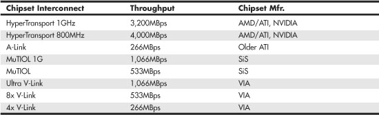
• VIA—VIA created the V-Link architecture to connect its North and South Bridge chips at speeds matching or exceeding Intel hub architecture. V-Link uses a dedicated 8-bit data bus and is currently implemented in three versions: 4x V-Link, 8x V-Link, and Ultra V-Link. 4x V-Link transfers data at 266MBps (4×66MHz), which is twice the speed of PCI and matches the speed of Intel’s AHA and HI 1.5 hub architectures. 8x V-Link transfers data at 533MBps (4×133MHz), which is twice the speed of Intel’s AHA interface. Ultra V-Link transfers data at 1GBps, which is four times the speed of Intel’s AHA interface and equals the speed of Intel’s current DMI hub architecture.
• SiS—SiS’s MuTIOL architecture (also called HyperStreaming) provides performance comparable to VIA’s 4x V-Link; the second-generation MuTIOL 1G used in SiS’s chipsets provides performance comparable to VIA’s Ultra V-Link and Intel’s DMI architectures. Chipsets that support MuTIOL use separate address, DMA, input data, and output data buses for each I/O bus master. MuTIOL buffers and manages multiple upstream and downstream data transfers over a bidirectional 16-bit data bus.
• ATI—ATI (now owned by AMD) used a high-speed interconnect called A-Link in its 9100-series IGP integrated chipsets. A-Link runs at 266MBps, matching Intel’s AHA interface as well as first-generation V-Link and MuTIOL designs. However, ATI now uses the HyperTransport bus for its current chipsets.
• NVIDIA—NVIDIA’s nForce chipsets use the HyperTransport bus originally developed by AMD.
Table 4.9 compares the performance features and chipset support of major non-Intel high-speed chipset architectures.
Table 4.9 Non-Intel High-speed Chipset Interconnect Architectures
Let’s examine the popular chipsets used from the 486 to the present.
Intel’s Early 386/486 Chipsets
Intel’s first real PC motherboard chipset was the 82350 chipset for the 386DX and 486 processors. This chipset was not very successful, mainly because the EISA bus was not very popular and many other manufacturers were making standard 386 and 486 motherboard chipsets at the time. The market changed very quickly, and Intel dropped the EISA bus support and introduced follow-up 486 chipsets that were much more successful.
Table 4.10 shows the Intel 486 chipsets.
Table 4.10 Intel 486 Motherboard Chipsets

The 420 series chipsets were the first to introduce the North/South Bridge design that is still used in many chipsets today.
Fifth-Generation (P5 Pentium Class) Chipsets
With the advent of the Pentium processor in March 1993, Intel also introduced its first Pentium chipset: the 430LX chipset (code-named Mercury). This was the first Pentium chipset on the market and set the stage as Intel took this lead and ran with it. Other manufacturers took months to a year or more to get their Pentium chipsets out the door. Since the debut of its Pentium chipsets, Intel has dominated the chipset market for Intel processors. Table 4.11 shows the Intel Pentium motherboard chipsets. Note that none of these chipsets support AGP; Intel first added support for AGP in its chipsets for the Pentium II/Celeron processors.
Table 4.11 Intel Pentium Motherboard Chipsets (North Bridge)

Note
PCI 2.1 and later supports concurrent PCI operations, enabling multiple PCI cards to perform transactions at the same time for greater speed.
Table 4.12 shows the Intel South Bridge chips used with Intel chipsets for Pentium processors. South Bridge chips are the second part of the modern Intel motherboard chipsets.
Table 4.12 Intel South Bridge Chips
The Pentium chipsets listed in Tables 4.11 and 4.12 have been out of production for several years, and most computers that use these chipsets have been retired.
Sixth-Generation (P6 Pentium Pro/II/III Class) Chipsets
Because the Pentium Pro, Celeron, and Pentium II/III were essentially the same processor with different cache designs and minor internal revisions, the same chipset can be used for Socket 8 (Pentium Pro), Socket 370 (Celeron/Pentium III), and Slot 1 (Celeron/Pentium II/III) designs.
Table 4.13 shows the chipsets used on Pentium Pro motherboards.
Table 4.13 Pentium Pro Motherboard Chipsets (North Bridge)

Note
PCI 2.1 supports concurrent PCI operations.
For the Celeron and Pentium II/III motherboards, Intel offered the chipsets in Table 4.14. 4xx series chipsets incorporate a North/South Bridge architecture, whereas 8xx series chipsets support the newer and faster hub architecture. P6/P7 (Pentium III/Celeron, Pentium 4, and Xeon) processor chipsets using hub architecture are shown in Table 4.15.
Table 4.14 P6 Processor Chipsets Using North/South Bridge Architecture
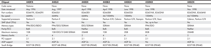
Table 4.15 P6 (Pentium III/Celeron) Processor Chipsets Using Hub Architecture

Note
Pentium Pro, Celeron, and Pentium II/III CPUs have their secondary caches integrated into the CPU package. Therefore, cache characteristics for these machines are not dependent on the chipset but are quite dependent on the processor instead.
Most Intel chipsets are designed as a two-part system, using a North Bridge (MCH or GMCH in hub-based designs) and a South Bridge (ICH in hub-based designs) component. Often the same South Bridge or ICH component can be used with several different North Bridge (MCH or GMCH) chipsets. Table 4.16 shows a list of all the Intel South Bridge components used with P6-class processors and their capabilities. The ICH2 is also used as part of some of the first seventh-generation (Pentium 4/Celeron 4) Intel chipsets.
Table 4.16 Intel South Bridge-I/O Controller Hub Chips for P6
Several third-party companies also produced chipsets designed to support P6-class processors, including ALi Corporation (formerly known as Acer Laboratories), VIA Technologies, and SiS. ALi (Acer Labs, Inc.) spun off its chipset division in 2003 as ULi Electronics; then ULi was acquired by NVIDIA in 2006. ALi manufactured a variety of chipsets for the P6-class processors. Most of these were similar in form and function to the Intel offerings.
Seventh/Eighth-Generation (Pentium 4/D, Core 2, and Core i) Chipsets
The Pentium 4 and Celeron processors using Socket 423 and those made for Socket 478 are essentially the same processors with different cache designs and minor internal revisions, so the same chipset can be used for both processors. The Pentium 4 processor in Socket 775 is very different from its predecessors; consequently, most 9xx-series chipsets support only the Socket 775 version of the Pentium 4, as well as the newer Core 2 series of processors.
Tables 4.17 and 18 show the 8xx-series chipsets made by Intel for Pentium 4 and Celeron 4 processors. These chipsets use Intel’s hub architecture, providing an interconnect speed of 266MBps between the MCH/GMCH and the ICH chips.
Table 4.17 Pentium 4 8xx-Series Chipsets from Intel Introduced 2000–2002

Table 4.18 Intel 8xx-Series Chipsets Introduced in 2003 for Pentium 4

Table 4.19 lists the ICH chips used by 8xx-series Pentium 4/Celeron 4 chipsets made by Intel.
Table 4.19 I/O Controller Hub Chips for Pentium 4 8xx-Series Chipsets

In mid-2004, Intel introduced the 915/925 series of chipset for the Pentium 4 and Celeron 4. These chipsets, code-named Grantsdale and Alderwood before their introduction, are the first Intel chipsets to support several Socket 775 processors, DDR2 memory and PCI Express for both video and other high-speed I/O uses (such as Gigabit Ethernet).
In 2005, Intel introduced its first dual-core chip for desktop processors (the Pentium D) as well as a processor designed for maximum single-core performance (the Pentium Extreme Edition). To support these new processors as well as Socket 775 Pentium 4 processors with HT Technology, Intel released the 945, 955, and 975 chipsets.
Because of the greater performance needed to support these high-speed technologies, the 9xx-series chipsets use a faster hub architecture than what was used by the 8xx-series chipsets. The new interconnect design, known as Direct Media Interface (DMI), runs at 1GBps in each direction. Table 4.20 lists the 9xx-series chipsets for the Pentium 4; Table 4.21 lists the 9xx-series chipsets for the Core 2, Pentium D, and Pentium Extreme Edition (they also support the Pentium 4); and Table 4.22 lists the ICH6 and ICH7 families of I/O controller hub chips used with 9xx-series chipsets.
Table 4.20 Intel 9xx-Series Chipsets for Pentium 4

Table 4.21 Intel 9xx-Series Chipsets for Core 2, Pentium D, Pentium Extreme Edition, and Pentium 4

Table 4.22 Intel 9xx Chipset I/O Controller Hub (ICH) Specifications (aka South Bridge)

Intel 915 Family
The Intel 915 chipset family, code-named Grantsdale during its development, was introduced in 2004. The Grantsdale family comprises six members (910GL, 915PL, 915P, 915G, 915GV, and 915GL), all of which support the 90nm Pentium 4 Prescott core. These chipsets are the first to support the Socket 775 processor interface outlined in Chapter 3. These chipsets are intended to replace the 865 Springdale family of chipsets.
The 915P, 915G, 915GV, 915GL, and 915PL models are all designed to support the HT Technology feature built into most recent Pentium 4 processors and to support bus speeds up to 800MHz. All five chipsets support dual-channel DDR memory up to 400MHz and PCI Express x1 and as well as PCI version 2.3 expansion slots. The 915P, 915G, and 915GV chipsets also support the new DDR2 memory standard at speeds up to 533MHz.
The 915P and 915PL use a PCI Express x16 slot for high-speed graphics, whereas the 915G has a PCI Express x16 slot as well as integrated Intel Graphics Media Accelerator 900 (originally known as Extreme Graphics 3). The 915GV, 915GL, and 910GL use Intel Graphics Media Accelerator 900 but do not include a PCI Express x16 slot. Graphics Media Accelerator 900 is a partial implementation of DirectX 9, but it lacks the vertex shaders found on fully compatible DirectX 9 GPUs from ATI and NVIDIA.
The 910GL is the low-end member of the family, lacking support for DDR2 RAM, 800MHz bus speeds, and PCI Express x16 video. The 910GL is designed to be matched with Intel Celeron or the Celeron D processors to produce a low-cost system.
All 915-series MCH/GMCH chips use the new ICH6 family of South Bridge (I/O Controller Hub or ICH) replacements detailed in Table 4.22.
Intel 925X Family
The Intel 925 chipset family includes two members: the 925X and the 925XE. The Intel 925X chipset, code-named Alderwood, was released in 2004. It was designed to replace the 875P Canterwood chipset. Unlike the 915 series of chipsets, which continue to support older DDR memory, the 925X supports only DDR2 memory. The 925X also supports ECC memory, providing a fast and accurate platform for mission-critical applications. To further improve performance, it uses an optimized memory controller design.
The 925X supports the Pentium 4 Extreme Edition and the Pentium 4 in Socket 775 form factors. It also includes PCI Express x1, PCI Express x16 (video), and PCI version 2.3 expansion slots. The I/O controller hub uses the ICH6 family of South Bridge replacements detailed in Table 4.22.
The 925XE is an updated version of the 925X, adding support for 1,066MHz FSB speeds; however, it dropped support for the Pentium 4 Extreme Edition processor and for ECC memory.
Intel 945 Express Family
The Intel 945 Express chipset family (code-named Lakeport) was released in 2005 and includes three members: the 945G, 945P, and 945PL. These chipsets, along with the 955X and 975X, are the first to support Intel’s new dual-core Pentium D processors, but they also support Pentium 4 HT Technology processors using Socket 775.
The 945G and 945P are aimed at what Intel refers to as the “performance PC” market segment. They offer FSB speeds up to 1,066MHz and up to 4GB of dual-channel DDR2 memory (two pairs) running at up to 667MHz. Both feature PCI Express x16 support, but the 945G also incorporates Intel Graphics Media Accelerator 950 integrated graphics.
The 945PL—aimed at what Intel refers to as the “mainstream PC” segment—supports only two memory modules (one pair of dual-channel modules) running at up to 533MHz and a maximum memory size of 2GB. It also supports PCI Express x16.
All members of the 945 family support the ICH7 family of I/O controller hub chips listed in Table 4.22. The ICH7 family differs from ICH6 in the following ways:
• It has support for 300MBps Serial ATA.
• It has support for SATA RAID 5 and Matrix RAID (ICH7R only).
• It has support for two additional PCI Express x1 ports (ICH7R only).
Figure 4.22 compares the features of the 945G and 915G chipsets.
Figure 4.22 The 915G chipset (left) was the first Intel chipset to support both PCI Express x16 and integrated graphics. The 945G chipset (right) offers similar features but supports faster integrated graphics, faster SATA hard disks, and more PCI Express x1 slots than the 915G.
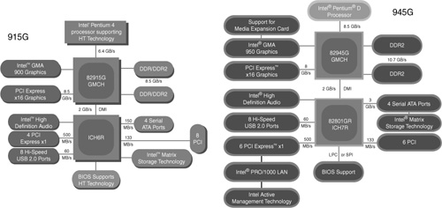
Intel 955X and 975X Family
The Intel Glenwood chipset family was released in 2005 and includes two members: the 955X and 975X. These chipsets, along with the 945 family, are the first to support Intel’s new dual-core Pentium D processors, but they also support the new high-performance single-core Pentium Extreme Edition processors as well as existing Pentium 4 HT Technology processors using Socket 775. Intel categorizes these chipsets as entry-level workstation and performance PC chipsets.
Although these chipsets are numbered in different series, most of their features are identical. Both support FSB speeds of 800MHz and 1,066MHz and support up to four DDR2 667/533MHz memory modules (two pairs of dual-channel modules) for a maximum 8GB of system memory. Both support ECC memory—a must for workstation operation—and both use the ICH7 family of I/O controller hub chips listed in Table 4.22.
The 955X and 975X differ from each other in their video support. The 955X supports a single PCI Express x16 video card, whereas the 975X supports two PCI Express video cards in CrossFire dual-slot operation.
Intel 96x Series
The 96x series (code-named Broadwater) was introduced in June 2006 and is designed to support the Core 2 processors, including dual- and quad-core versions. There are several models in the series, each with slightly different features. The Q963 and Q965 are the most basic versions. Both feature integrated GMA 3000 video; however, the Q965 includes support for a PCIe x16 slot (allowing for a video card upgrade). It also supports faster 800MHz DDR2 memory. The P965 deletes the integrated video for those only wanting to use PCIe x16 cards. Finally, the G965 includes all the features of the other chipsets while adding even better integrated GMA X3000 video, along with support for a PCIe x16 upgrade slot. Table 4.23 shows the major features of these chipsets.
Table 4.23 Intel 96x Chipsets for Core 2

Intel 3x and 4x Series Chipsets
First introduced in June 2007, the 3x series chipset family (code-named Bearlake) is designed to support the Core 2 processors in both dual- and quad-core versions. The 4x series followed in March 2008, and basically added DDR3 memory support, plus faster PCIe 2.x slots and improved integrated graphics.
Some of the 3x and 4x series chipsets also include integrated GMA (Graphics Memory Accelerator) graphics, and some of those include Clear Video Technology, which can enhance video playback and support the High Definition Media Interface (HDMI).
The 3x and 4x series are available in a number of versions, including some with integrated video, support for faster CPU and memory speeds, as well as more memory and slots. Table 4.24 and 4.25 show the different 3x and 4x series chipsets.
Table 4.24 Intel 3x Chipset Specifications
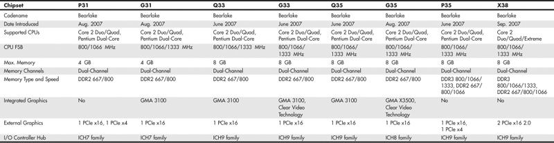
Table 4.25 Intel 4x Chipset Specifications
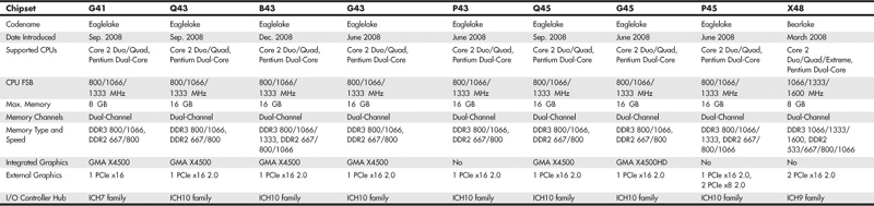
The 3x and 4x series chipsets are designed as a two-chip set solution, and must be combined with a corresponding ICH (I/O Controller Hub) chip. The ICH contains interfaces for the SATA ports (some with RAID capability), non-video PCIe slots, USB ports and integrated HD audio and LAN connections. Table 4.26 shows the specific ICH chips that are used with 3x and 4x series chipsets.
Table 4.26 Intel 3x/4x/5x Chipset I/O Controller Hub (ICH) Specifications (aka South Bridge)

Intel 5x Series Chipsets
The Intel 5x series of chipsets are designed to support the Core i Series processors. These processors and chipsets have a distinctly different design from previous Intel chipsets, and represent a new level of system integration. In fact the 5x series actually has two completely different sub-series, with the first two examples being the X58 IOH (I/O Hub) introduced in November 2008, and the P55 PCH (Platform Controller Hub) introduced in September 2009.
Perhaps the biggest difference between the 5x series chipsets and its predecessors is that the memory controller is no longer part of the chipset, having been moved directly into the Core i Series processors instead. Placing the memory controller in the processor means that the memory modules are directly connected to the processor instead of the North Bridge chipset component, allowing for a dedicated connection between the processor and memory. While this sounds like (and is) a good idea, it’s not a new idea. This is something that AMD first introduced in the Athlon 64 as far back as 2003.
With the memory controller integrated into the processor, the only function left for the north bridge is to act as an interface to the PCIe video card slots. Because the North Bridge no longer controls memory, Intel changed the name from MCH (Memory Controller Hub) to IOH (I/O Hub) in the 5x series chipsets that support socket LGA1366 processors. Figure 4.23 shows the block diagram of a system with a socket LGA1366 Core i Series processor on a motherboard with an X58 Express chipset. In the diagram you can also see the use of the traditional ICH (I/O Controller Hub), which supports interfacing to SATA, USB, and other components in the system.
Figure 4.23 Block diagram of a system with a socket LGA1366 Core i Series processor and an X58 Express chipset.
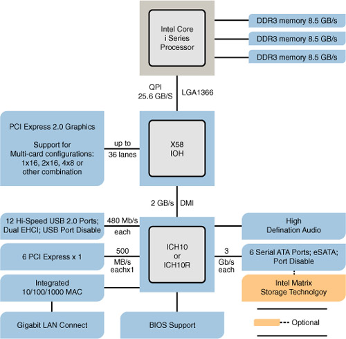
Currently the only 5x series chipset for socket LGA1366 processors is the X58 Express, for which Table 4.27 lists the features.
Table 4.27 Intel 5x Chipset for Socket LGA1366 Processors

In systems using socket LGA1156 Core i Series processors, Intel has taken this component consolidation even further by incorporating not only the memory controller, but also the PCI Express video interface directly into the processor. In effect this means that Intel has built the entire north bridge part of the chipset right into the processor, reducing the motherboard chipset from two chips down to one. The remaining south bridge chip has the same functions as what Intel previously called the ICH (I/O Controller Hub), but to differentiate it from previous designs, they have changed the designation to PCH (Platform Controller Hub) instead.
Figure 4.24 shows the block diagram of a system with a socket LGA1156 Core i Series processor on a motherboard with an P55 chipset. In the diagram you can see that the functionality of the north bridge is now part of the CPU, reducing the chipset to a single south bridge (now called PCH) component.
Figure 4.24 Block diagram of a system with a socket LGA1156 Core i Series processor and a P55 chipset.

By building the external video interface directly into the processor, Intel is also able to produce processors with integrated graphics processing. Several of the new 5x series chipsets (such as the H55, H57, and Q57) support the FDI (Flexible Display Interface), which requires a Core i Series processor with integrated graphics. Using FDI, video signals are sent from the GPU in the processor to the PCH, which then implements the physical interface to the display (i.e. DisplayPort, HDMI, DVI, and/or VGA). Table 4.28 shows the 5x series chipsets for socket LGA1156 Core i Series processors.
Table 4.28 Intel 5x Chipsets for Socket LGA1156 Core i Series Processors
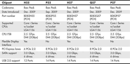
Third-party Chipsets for Intel Processors
SiS, ULi (now NVIDIA), ATI, and VIA have all produced chipsets for the Intel Pentium 4/D and Core 2 processors.
Although Intel’s chipsets have dominated the market up to this point, many of these chipsets offer unique features that are worth considering. The following sections discuss the more popular versions of these chipsets by vendor.
SiS Chipsets
SiS offers several chipsets for Intel processors, including integrated chipsets, chipsets for use with discrete video accelerator cards, and some that support Rambus RDRAM. Details of SiS’s chipsets for the Pentium 4 are available in Tables 4.29–4.32; chipsets for the Pentium D are listed in Tables 4.31 and 4.32. Unlike most of the chipsets SiS has created for the Pentium II/III/Celeron, the SiS chipsets for the Pentium 4 and Pentium D use one of several high-speed South Bridge equivalents (SiS 96x series Media I/O chips) instead of integrating North and South Bridge functions into a single chip. SiS North and South Bridge chips for the Pentium 4 and Pentium D use a high-speed 16-bit connection known as MuTIOL (Multi-Threaded I/O Link) instead of the slow PCI bus as with older chipsets.
Table 4.29 SiS North Bridge Chips for Pentium 4 Socket 478 (Up to 533MHz Processor Bus Speed)

Table 4.30 SiS North Bridge Chips for Pentium 4 (800MHz Processor Bus Speed)
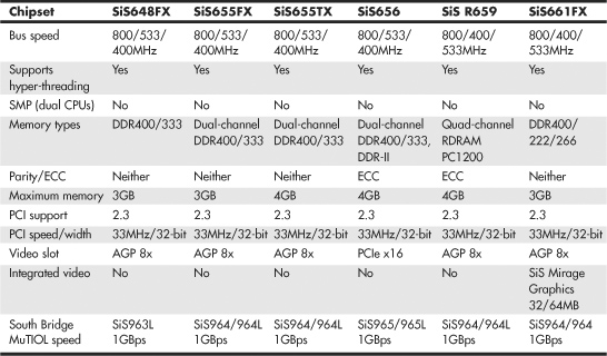
Table 4.31 SiS North Bridge Chips for Pentium D and Pentium 4 (Socket 775)

Table 4.32 SiS Media I/O (South Bridge) Chips for Intel and AMD Processors
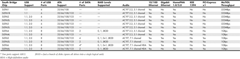
ULi Electronics Chipsets
ULi Electronics (formerly known as ALi Corporation and Acer Laboratories, and later acquired by NVIDIA) has produced several chipsets for the Pentium 4 and Celeron 4 processors. Tables 4.33 and 4.34 provide an overview of these chipsets.
Table 4.33 ULi Chipsets for Pentium 4

Table 4.34 ULi South Bridge Chips for Pentium 4, Athlon XP, and Athlon 64
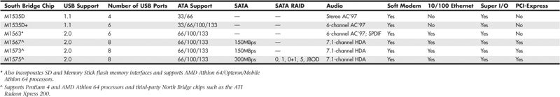
Table 4.34 provides an overview of the ULi South Bridge chips used in ULi’s chipsets for the Pentium 4; some of these South Bridge chips also support the Athlon XP and Athlon 64 processors from AMD.
ATI Chipsets
ATI’s original line of chipsets for the Pentium 4 integrate Radeon VE-level 3D graphics, DVD playback, and dual-display features with high-performance North Bridge and South Bridge designs. ATI uses its high-speed A-Link bus to connect its North and South Bridge chips.
The Radeon IGP North Bridge chips for Pentium 4 include the ATI A4 family, composed of the IGP 330 and IGP 340.
The Radeon 9x00 IGP family is ATI’s second generation of chipsets for the Pentium 4. The 9x00 IGP North Bridge chips feature Radeon 9200-level graphics with DirectX 8.1 hardware support and support for multiple monitors. On the other hand, the companion IXP 300 South Bridge supports Serial ATA and USB 2.0 as well as six-channel audio. The Radeon 9x00 IGP family includes the 9100 IGP, 9100 Pro IGP, and 9000 Pro IGP.
ATI’s current line of Pentium 4–compatible chipsets includes the RC410 (integrates Radeon X300 3D graphics) and the RS400 (integrates Radeon X300 3D graphics and includes support for PCI Express x16 video). Both are sold under the Radeon Xpress 200 brand name. Although ATI has made South Bridge chips in the past, its current Radeon Xpress 200 North Bridge chips can be paired with either ATI’s own IXP 450 or ULi’s M157x South Bridge chips. ATI’s South Bridge chips include the IXP 150, 200, 250, 300, 400, and 450.
Table 4.35 summarizes the major features of the North Bridge chips, and Table 4.36 summarizes the major features of the South Bridge chips used in ATI’s integrated chipsets for the Pentium 4. The Radeon IGP 330 and 340 chipsets were not widely used in desktop computers and have now been discontinued.
Table 4.35 Radeon IGP (North Bridge) Chips for Pentium 4

Table 4.36 ATI South Bridge Chips for Pentium 4
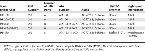
VIA Chipsets
Although VIA Technologies produces a line of chipsets for the Core 2 and Pentium 4, it initially lacked a license from Intel for the processor interface. This slowed acceptance of VIA’s chipsets by motherboard makers until VIA and Intel reached an agreement in April 2003. With the agreement between VIA and Intel, VIA’s chipsets for the Core 2 and Pentium 4 are now being used by several motherboard manufacturers.
Tables 4.37 and 4.38 provide an overview of VIA’s chipsets for the Pentium 4, including ProSavage chipsets with integrated graphics.
Table 4.37 VIA Chipsets for Pentium 4 (Up to 533MHz System Bus)

Table 4.38 VIA Chipsets for Core 2/Pentium 4 (800MHz+ System Bus)

Table 4.39 lists the major features of the VIA South Bridge chips used in VIA’s chipsets. Note that these same chips are also used by VIA chipsets for the AMD Athlon family of processors. All chipsets that use these South Bridge chips use VIA’s high-speed V-Link interface between North and South Bridge chips. These chipsets connect to the VT1211 LPC (low pin count) or equivalent Super I/O chip for support of legacy devices such as serial, IR, and parallel ports and the floppy drive.
Table 4.39 VIA South Bridge Chips

VIA’s North and South Bridge chips for the Pentium 4 support VIA’s Modular Architecture Platforms (V-MAP) designs, which enable motherboard designers to convert quickly to more advanced versions of a chipset because of a common pinout. Therefore, motherboards using these chipsets can be built in a variety of configurations. All these chipsets also support VIA’s V-Link high-speed connection between the North and South Bridge chips.
AMD Athlon Chipsets
The original AMD Athlon was a Slot A processor chip, but subsequent versions used Socket A—as do the Athlon XP, Duron, and some versions of the Sempron. Although similar in some ways to the Pentium III and Celeron, the AMD chips use a different interface and require different chipsets. AMD was originally the only supplier for Athlon chipsets, but VIA Technology, ULi Electronics, SiS, and NVIDIA produced a large number of chipsets with a wide range of features. These chipsets are covered in the following sections.
AMD Chipsets
AMD makes four chipsets for Athlon and Duron processors: the AMD-750 and AMD-760/MP/MPX. The major features of these chipsets are compared in Table 4.40 and described in greater detail in the following sections.
Table 4.40 AMD Athlon/Duron Processor Chipsets Using North/South Bridge Architecture

VIA Chipsets for AMD
VIA Technologies, Inc., is the largest chipset and processor supplier outside of Intel and AMD. Originally founded in 1987, VIA is based in Taipei, Taiwan, and is the largest integrated circuit design firm on the island. VIA is a fabless company, which means it farms out the manufacturing to other companies with chip foundry capability. Although it is best known for its chipsets, in 1999 VIA purchased the Cyrix processor division from National Semiconductor and the Centaur processor division from IDT, respectively, thereby becoming a supplier of processors in addition to chipsets. VIA has also formed a joint venture with SONICblue (formerly S3) as a means of integrating graphics capabilities into various chipset products. This joint venture is known as S3 Graphics Co., Ltd.
VIA makes chipsets for Intel, AMD, and Cyrix (VIA) processors. Table 4.41 provides an overview of VIA’s Athlon/Duron chipsets that use the traditional North/South Bridge architecture.
Table 4.41 VIA Athlon/Duron/Athlon XP Processor Chipsets Using North/South Bridge Architecture

VIA eventually converted to an architecture called V-Link, which uses a fast dedicated connection between the North Bridge and South Bridge. V-Link is similar to Intel’s hub architecture, as well as HyperTransport (used by ALi, NVIDIA, and ATI), MuTIOL (used by SiS) and A-Link (used by ATI). V-Link is also used by VIA’s Pentium 4 chipsets. Table 4.42 provides an overview of V-Link chipsets, which also support the VIA Modular Architecture Platform (V-MAP) design. As with VIA’s chipsets for the Pentium 4, V-MAP uses identical pinouts for several ranges of V-Link North and South Bridge chips so vendors can reuse a motherboard design with more advanced chipsets as they are developed. Details regarding VIA’s South Bridge chips for Athlon processors are summarized in Table 4.43.
Table 4.42 VIA Athlon XP/Duron Processor Chipsets Using V-Link Architecture

Table 4.43 VIA South Bridge Chips for Athlon/Duron/Athlon XP

SiS Chipsets for AMD
SiS has a variety of chipsets for the Athlon, Duron, and Athlon XP processors. Tables 4.44 and 4.45 provide an overview of these chipsets, some of which use a single-chip design and others of which use a high-speed two-chip design similar to other vendors’ chipsets.
Table 4.44 SiS Chipsets for Athlon/Duron/Athlon XP Processors


Table 4.45 SiS MuTIOL South Bridge Chips for Athlon XP

The SiS96x-series South Bridge chips use a high-speed bus called MuTIOL to connect with compatible North Bridge chips. The original version of MuTIOL (supported by the SiS961- and 962-series chips) is a 16-bit-wide 266MHz connection that provides 533MBps bandwidth, twice the speed of the Intel hub architecture used by Intel’s 800-series chipsets.
The SiS963, 964, and 965 series and matching North Bridge chips use a second generation of MuTIOL called MuTIOL 1G, which supports a 16-bit-wide 533MHz connection to achieve bandwidths exceeding 1GBps.
When connected to the SiS746FX, SiS741GX, SiS748, or SiS741 North Bridge chip and newer models, the SiS963/964 series chips use a further development of MuTIOL called HyperStreaming, which integrates the following four technologies to further improve the speed of data transfer:
• Single Stream with Low Latency Technology—Improves performance by 5%–43%, depending on the activity.
• Multiple Stream with Pipelining and Concurrent Execution Technology—Uses concurrent parallel data pipelines and simultaneous processing of nonsequential data. In file-copy operations, for example, performance increases as data file size increases.
• Specific Stream with Prioritized Channel Technology—Improves playback of Internet music, video, and applications such as IP telephony and videoconferencing.
• Smart Stream Flow Control Technology—Analyzes characteristics of different interfaces and improves performance.
NVIDIA nForce Chipsets for AMD
NVIDIA, although best known for its popular GeForce line of graphics chipsets, also became a popular vendor of chipsets for the AMD Athlon/Duron/Athlon XP processor family thanks to its nForce and nForce2 product families.
Table 4.46 provides an overview of the North Bridge chips in the nForce and nForce2 families, and Table 4.47 provides an overview of the nForce/nForce2 South Bridge chips. The nForce is a descendant of the custom chipset NVIDIA created for the Microsoft Xbox console game system.
Table 4.46 nForce/nForce2 IGP/SPP (North Bridge) Chips

Table 4.47 nForce/nForce2 MCP (South Bridge) Chips

nForce North Bridge chips with integrated graphics are known as integrated graphics processors (IGPs), whereas those that require separate AGP video are known as system platform processors (SPPs). All South Bridge chips are known as media and communications processors (MCPs). IGP/SPP and MCP chips communicate over an 800MBps HyperTransport connection.
The combination of advanced memory controllers, prefetch design, HyperTransport high-speed connection, and hardware audio processing in MCP-D and MCP-T chips makes the second-generation nForce2 chipsets among the fastest chipsets available for Athlon XP processors. The new Gigabit MCP and RAID MCP chips bring eight-port USB 2.0 and Serial ATA/ATA RAID support to nForce2-based systems. The Gigabit MCP is the first nForce2 MCP chip to offer integrated Gigabit Ethernet.
Figure 4.25 shows the architecture of the nForce2 IGP and MCP-T combination, which provides the greatest versatility. If the SPP North Bridge is used instead of the IGP, integrated video is not present. If the MCP South Bridge is used instead of the MCP-T, then IEEE 1394a, hardware 5.1 Dolby Digital audio, and dual network ports are not available.
Figure 4.25 NVIDIA nForce2 IGP/MCP2 chipset architecture.
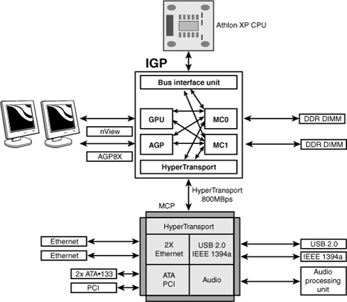
ATI Radeon IGP Chipsets
Before AMD’s acquisition of the company, ATI made a series of chipsets for the Athlon series of processors that integrated Radeon VE-level 3D graphics, DVD playback, and dual-display features with high-performance North Bridge and South Bridge designs. These chipsets use ATI’s high-speed A-Link bus to connect its North and South Bridge chips, but they also support connections to third-party South Bridge chips via the PCI bus. This has enabled system designers to create an all-ATI or a mix-and-match solution. Many of the first Radeon IGP-based systems on the market used ALi (now ULi) or VIA South Bridge chips. The Radeon IGP 320 North Bridge chip can be matched with either of ATI’s South Bridge chips: the IXP 200 or IXP 250. Both of these chips support six USB 2.0 ports and ATA33/66/100. The Radeon 320 IGP is now discontinued. Table 4.48 summarizes the major features of the IGP 320, and Table 4.49 summarizes the major features of the IXP 200 and 250.
Table 4.48 Radeon IGP (North Bridge) Chip for Athlon

Table 4.49 ATI South Bridge Chips for Athlon

AMD Athlon 64 Chipsets
The Athlon 64 processor requires a new generation of chipsets, both to support its 64-bit processor architecture and to allow for integration of the memory controller into the processor (the memory controller has traditionally been located in the North Bridge chip or equivalent). As a consequence, some vendors do not use the term North Bridge to refer to the chipset component that connects the processor to AGP video.
AMD (ATI), VIA Technologies, NVIDIA (ULi/ALi) and SiS have developed chipsets for the Athlon 64.
AMD 8000 (8151) Chipset
The AMD 8000 is AMD’s first chipset designed for the Athlon 64 and Opteron families. Its architecture is substantially different from the North Bridge/South Bridge or hub-based architectures we are familiar with from the chipsets designed to support Pentium II/III/4/Celeron and AMD Athlon/Athlon XP/Duron processors.
The AMD-8000 chipset is often referred to as the AMD-8151 because the AMD-8151 provides the connection between the Athlon 64 or Opteron processor and the AGP video slot—the task usually performed by the North Bridge or MCH hub in other chipsets. The name of the North Bridge or MCH hub chip is usually applied to the chipset. However, AMD refers to the AMD-8151 chip as the AGP Graphics Tunnel chip because its only task is to provide a high-speed connection to the AGP slot on the motherboard. The other components of the AMD-8000 chipset include the AMD-8111 HyperTransport I/O hub (South Bridge) and the AMD-8131 PCI-X Tunnel chip.
Due to delays in the development of the AMD-8151 AGP Graphics Tunnel chip, most vendors through late 2003 used the AMD-8111 HyperTransport I/O hub alone or along with the AMD-8131 PCI-X Tunnel chip to provide a mixture of PCI and PCI-X slots on motherboards optimized as servers. Some recent systems have incorporated the AMD-8151 chip to provide AGP video, but the AMD-8000 chipset continues to be used primarily as a workstation/server chipset instead of as a desktop chipset.
The AMD-8151 AGP Graphics tunnel has the following major features:
• Supports AGP 2.0/3.0 (AGP 1x–8x) graphics cards
• 16-bit up/down HyperTransport connection to the processor
• 8-bit up/down HyperTransport connection to downstream chips
The AMD-8111 HyperTransport I/O hub (South Bridge) chip’s major features include
• PCI 2.2-compliant PCI bus (32-bit, 33MHz) for up to eight devices
• AC’97 2.2 audio (six-channel)
• Six USB 1.1/2.0 ports (three controllers)
• Two ATA/IDE host adapters supporting up to ATA-133 speeds
• RTC
• Low-pin-count (LPC) bus
• Integrated 10/100 Ethernet
• Eight-bit up/down HyperTransport connection to upstream chips
The AMD-8131 HyperTransport PCI-X tunnel chip’s major features include
• Two PCI-X bridges (A and B) supporting up to five PCI bus masters each
• PCI-X transfer rates up to 133MHz
• PCI 2.2 33MHz and 66MHz transfer rates
• Independent operational modes and transfer rates for each bridge
• Eight-bit up/down HyperTransport connection to upstream and downstream chips
Figure 4.26 shows the architecture of the AMD-8151 chipset for Athlon 64.
Figure 4.26 Block diagram of the AMD 8000 chipset for Athlon 64.

ATI (AMD)
One of the expectations of AMD’s acquisition of ATI in 2006 was the release of AMD/ATI chipsets for AMD processors. Since then, several chipsets have been released to support the Athlon 64, Sempron and Phenom processors. Table 4.50 summarizes the major features of these chipsets, while Table 4.51 covers the corresponding south bridge components
Table 4.50 AMD/ATI Chipsets for Phenom, Athlon 64, and Sempron Processors

Table 4.51 AMD/ATI Chipset South Bridge Components

VIA Chipsets for Athlon 64
VIA has long been one of the leading developers of chipsets for AMD processors, and this pattern continues with the Athlon 64 and Opteron. VIA offers five chipsets for these processors: K8T800 Pro, K8T800, K8M800, K8T890, and K8M890.
The following sections cover these chipsets in more detail.
K8T800, K8T800 Pro, and K8M800
The K8T800 (originally known as the K8T400) was VIA’s first chipset for the Athlon 64 and Opteron processors. It departs somewhat from the pattern established by AMD’s and ALi’s chipsets by using VIA’s own 8x V-Link (533MBps) interconnect between the North and South Bridge chips instead of HyperTransport (although HyperTransport is used, of course, to connect to the processor). The K8T800 uses the VT8237 South Bridge chip.
The K8M800 is based on the K8T800 but adds S3 UniChrome Pro integrated graphics. UniChrome Pro offers a 128-bit 2D/3D engine, dual pixel pipelines, hardware acceleration for MPEG-2 and MPEG-4 video, and support for HDTV (up to 1080p) and standard TV as well as LCD and CRT displays.
K8T890, K8M890, and K8T900
The VIA K8T890 and K8M890 are VIA’s first PCI Express chipsets for the Athlon 64 and Opteron. These chipsets use the 1GHz HyperTransport processor/NB connection and Ultra V-Link NB/SB connections. These North Bridge chips actually have a 20-lane-wide PCI Express interface, leaving four lanes available for PCI Express x1 cards.
These chipsets are also designed to use the new VT8251 South Bridge, which includes several features that once required add-on chips:
• Four Serial ATA host adapters are included to support SATA RAID 0, 1, and 0+1.
• Support for Intel’s High-Definition Audio (HDA, formerly code-named Azalia) standard. HDA provides Dolby Digital IIfx–compatible (7.1) surround sound and 24-bit/192KHz sampling rates for CE-quality sound.
• Two PCI Express x1 slots, for a total of six possible (four connected to North Bridge and two to South Bridge).
Because of delays in production, some systems using the K8T890 and K8M890 used the earlier VT8237R South Bridge instead of the VT8251. Be sure to check specifications for a particular motherboard to determine which South Bridge chip was used.
The K8M890 adds integrated S3 Graphics DeltaChrome 2D/3D graphics with DirectX 9 graphics support to the features of the K8T890.
The K8T900 is based on the K8T890 but adds support for PCI Express 2 x8 video to support two PCI Express graphics cards.
NVIDIA Chipsets for Athlon 64
NVIDIA offers more than 14 chipset variations that support a range of Athlon 64, Sempron, and Opteron processors.
NVIDIA refers to these chips as media and communications processors (MCPs) because a single chip combines the functions of typical North and South Bridge chips. The following sections cover these chips in more detail.
nForce3 150 and nForce3 Pro 150
The NVIDIA nForce3 150 MCP was one of the first chipsets available for the Athlon 64 processor. Although it departs from the two-chip chipset standard used by most Athlon 64 chipsets by combining North Bridge and South Bridge functions, the nForce3 150 has a limited feature set. The short list of features reflects both this chipset’s early development and its positioning as an entry-level chipset.
The nForce3 Pro 150 is similar but is designed for use with the Opteron processor and NVIDIA’s Quadro workstation graphics processor.
nForce3 250, 250Gb, and 250 Ultra and nForce3 Professional 250
The nForce3 250 family of MCPs includes four members, all of which include several enhanced features over the original nForce3 150 and 150 Pro.
The 250Gb model has the 250’s features and adds support for 10/100/1000 Ethernet with integrated hardware firewall. The 250 Pro has the feature set of the 250 Gb but supports the Opteron workstation processor, and the Athlon 64FX and is optimized to work with NVIDIA’s Quadro workstation graphics processor.
The 250 Ultra model has the 250’s features and adds support for both 10/100/1000 Ethernet with integrated hardware firewall and an Advanced 16-bit/1GHz HyperTransport upstream/downstream processor/MCP connection.
nForce4 Series and nForce Professional Series
NVIDIA’s nForce4 series combines PCI Express support with the successful single-chip design used by the nForce3. The nForce4 series includes four models: the nForce4, nForce Ultra, nForce4 SLI, and nForce4 SI x16.
The base model, nForce4, has the following major features:
• HyperTransport 16-bit/800MHz upstream/downstream connections between the processor and the MCP
• PCI Express x16 graphics support
• Dual independent ATA-133 ATA/IDE host adapters with RAID 0, 1, and 0+1
• SATA and SATA RAID 0, 1, and 0+1
• Ten USB 1.1/2.0 ports
• 10/100/1000 Ethernet with integrated hardware firewall
• AC’97 2.1 audio (six-channel) with 20-bit output and SPDIF support
nForce4 Ultra adds support for 3Gbps SATA drives and the ActiveArmor secure networking edition.
nForce4 SLI supports a flexible PCI Express design that can use either a single x16 or two x8 NVIDIA PCI Express graphics cards. It also adds support for bootable RAID 5 to the features of nForce4 Ultra.
nForce4 SLI x16 supports one or two NVIDIA PCI Express x16 cards running at full speed and supports up to 38 total PCI Express lanes. Its other features are the same as the nForce4 SLI.
nForce4 Professional chipsets for the Opteron processors are based on the nForce4 series, but with the following differences:
• nForce Professional 2050 has x16 and four x1 PCI Express lanes; Gigabit Ethernet; and four SATA 3GBps ports with RAID 0,1 and 0+1 support. However, it offers no support for PATA drives, 32-bit PCI, audio, or the low-pin-count (LPC) bus used for legacy devices.
• nForce Professional 2200 has a flexible 20-lane PCI Express implementation; Gigabit Ethernet; and SATA 3GBps with RAID 0,1, and 0+1. However, it also supports 32-bit PCI, 10 USB 2.0 ports, the LPC bus, AC’97 2.3 audio, and four PATA drives. The 2200 is designed as a workstation processor. Both chipsets support multiple Opteron processors.
nForce 410 and 430 Series
The nForce 410 and 430 are the first NVIDIA chipsets with integrated video for the AMD Sempron, a 32-bit version of the Athlon 64. The nForce 410 and 430 use the GeForce 6100 GPU for integrated video, whereas the 430 can also use the GeForce 6150 GPU.
Table 4.52 lists the major features of each nForce 4xx-series integrated chipset.
Table 4.52 nForce 4xx Integrated Chipsets for AMD Sempron

SiS Chipsets for Athlon 64
SiS offers eight chipsets for 64-bit AMD processors. Of these, the 755, 755FX, and 756 require discrete graphics. SiS also offers the following chipsets with integrated graphics: 760, 760GX, 761, 761GX, and 761GL.
The following sections cover these chipsets in greater detail.
SiS755 and SiS755FX
The SiS 755 is the first SiS chipset to support the AMD Athlon 64, Opteron, and Athlon 64FX chipsets. It is a two-piece chipset that uses the SiS964 as its South Bridge component.
The 755FX North Bridge chip is pin-compatible with the 755; however, the preferred South Bridge chip for the 755FX—the SiS965—uses a larger 588-pin socket over the 505-pin socket used by the 964 family. The 755FX/965 chipset has the following major improvements over the 755/964 chipset:
• HyperTransport 16-bit/1GHz connection between the processor and North Bridge with HyperStreaming
• Support for two PCI Express x1 slots
• Four Serial ATA ports with SATA RAID 0, 1, and 0+1 and JBOD (disk spanning)
• 10/100/1000 Ethernet
SiS756
The SiS756 chipset is designed specifically for use with the high-performance Athlon 64FX desktop processor. It is the first SiS chipset to support the PCI Express x16 graphics interface. The SiS756 is usually paired with the SiS965 South Bridge.
PCI Express x16 replaces the AGP 8x video support found in earlier SiS chipsets.
Figure 4.27 shows the architecture of the SiS756 chipset with the SiS965 South Bridge.
Figure 4.27 As with most Athlon 64 chipsets, the SiS756’s North Bridge is used only for connection to discrete graphics (PCI Express in this case), while a vast majority of the work is performed by the South Bridge.
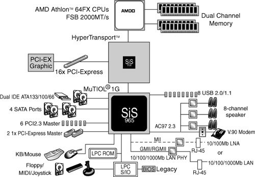
SiS760 and Sis760GX
The SiS760 is the first SiS chipset with integrated graphics for the Athlon 64 and Opteron processors. Otherwise, its major features are similar to those of the SiS755. Both use the SiS964 South Bridge chip.
The integrated SiS Mirage 2 (Ultra256) graphics features of the SiS760 include
• DirectX 8.1–compatible 3D graphics
• Dual-channel 256-bit 3D interface
• Optional support for TV-out and a secondary CRT or LCD display
• Shared memory up to 128MB
The SiS760GX instead uses Mirage 1 single-channel (128-bit) graphics.
The SiS966 South Bridge is the preferred South Bridge for the SiS760GX, adding the following features:
• Four PCI Express x1 slots
• SATA, SATA RAID 0, 1, and 0+1
• Ten USB 1.1/2.0 ports
• AC’97 2.3 audio with support for Intel’s new High Definition Audio 7.1-channel audio
• 10/100/1000 Ethernet
SiS761GL and SiS761GX
The SiS761GL and SiS761GX integrated graphics chipsets are based on the SiS760 and support all Athlon 64 processors, the Opteron, and the Sempron 32-bit version of the Athlon 64. Both chipsets use the SiS966 as their preferred South Bridge.
The SiS761GX North Bridge chip has the following major features:
• HyperTransport 16-bit/1GHz connection between the processor and North Bridge with HyperStreaming
• Support for PCI Express x16 graphics
• MuTIOL 1G connection between the North and South Bridge chips with HyperStreaming
• Integrated Mirage DirectX 7.0 graphics using up to 128MB of video memory
The SiS761GL differs from its sibling in these ways:
• HyperTransport 16-bit/800MHz
• No PCI Express x16 slot
• Integrated Mirage 1 DirectX 7.0 graphics using up to 128MB of video memory
When the SiS966 South Bridge chip is used, both chipsets also feature the following:
• Four PCI Express x1 slots
• SATA, SATA RAID 0, 1, and 0+1
• Ten USB 1.1/2.0 ports
• AC’97 2.3 six-channel audio with support for Intel’s High Definition Audio standard
Note
HDA, previously code-named Azalia, provides Dolby Pro Logic IIx-compatible 7.1-channel CE-quality (192KHz, 32-bit multichannel) sound.
• 10/100/1000 Ethernet
Super I/O Chips
The third major chip seen on many PC motherboards is called the Super I/O chip. This is a chip that integrates devices formerly found on separate expansion cards in older systems.
Most Super I/O chips contain, at a minimum, the following components:
• Floppy controller
• One or two serial port controllers
• Parallel port controller
The floppy controllers on some Super I/O chips handle two drives, but some newer models can handle only one. Older systems often required a separate floppy controller card.
The serial port is another item that was formerly on one or more cards. Most of the better Super I/O chips implement a buffered serial port design known as a universal asynchronous receiver transmitter (UART), one for each port. Most mimic the standalone NS16550A high-speed UART, which was created by National Semiconductor. Because the functions of these chips are put into the Super I/O chip, serial ports are essentially built into the motherboard.
Virtually all Super I/O chips also include a high-speed multimode parallel port. Most recent models allow three modes: standard (bidirectional), Enhanced Parallel Port (EPP), and the Enhanced Capabilities Port (ECP) modes. The ECP mode is the fastest and most powerful, but selecting it also causes your port to use an ISA bus 8-bit DMA channel—usually DMA channel 3. As long as you account for this and don’t set anything else to that channel (such as a sound card and so on), the ECP mode parallel port should work fine. Some of the newer printers and scanners that connect to the system via the parallel port use ECP mode, which was invented by Hewlett-Packard.
The Super I/O chip can contain other components as well. For example, the Intel VC820 ATX motherboard uses an SMC (Standard Microsystems Corp.) LPC47M102 Super I/O chip. This chip incorporates the following functions:
• Floppy drive interface
• Two high-speed serial ports
• One ECP/EPP multimode parallel port
• 8042-style keyboard and mouse controller
This chip is typical of recent Super I/O chips in that it has an integrated keyboard and mouse controller. Older Super I/O chips lacked this feature.
One thing I’ve noticed over the years is that the role of the Super I/O chip has decreased more and more in the newer motherboards. This is primarily due to Intel and other chipset manufacturers moving Super I/O functions, such as IDE, directly into the chipset South Bridge or ICH component, where these devices can attach to the PCI bus (North/South Bridge architecture) or to the high-speed hub interface (hub architecture) rather than the ISA bus. One of the shortcomings of the Super I/O chip is that originally it was interfaced to the system via the ISA bus and shared all the speed and performance limitations of that 8MHz bus. Moving the IDE over to the PCI bus allowed higher-speed IDE drives to be developed that could transfer at the faster 33MHz PCI bus speed.
Newer Super I/O chips interface to the system via the LPC bus, an interface designed by Intel to offer a connection running at half the speed of PCI (up to about 16.67MBps) using only 13 signals. LPC is much more efficient than ISA.
Because high-speed devices such as IDE/ATA drives are now interfaced through the South Bridge chip, PCI bus, or hub architectures, nothing interfaced through the current Super I/O chips needs any greater bandwidth anyway.
As the chipset manufacturers combine more and more functions into the main chipset, and as USB- and IEEE 1394–based peripherals replace standard serial, parallel, and floppy controller-based devices, we will probably see the Super I/O chip continue to fade away in motherboard designs. More and more chipsets are combining the South Bridge and Super I/O chips into a single component (often referred to as a Super South Bridge chip) to save space and reduce parts count on the motherboard. Several of the SiS and NVIDIA chipsets even integrate all three chips (North Bridge, South Bridge, and Super I/O) into a single chip.
![]() For more details on the CMOS RAM addresses, see “Motherboard CMOS RAM Addresses,” p. 337 (Chapter 5, “BIOS”).
For more details on the CMOS RAM addresses, see “Motherboard CMOS RAM Addresses,” p. 337 (Chapter 5, “BIOS”).
Motherboard Connectors
A modern motherboard contains a variety of connectors. Figure 4.28 shows the connector locations on a typical motherboard. Several of these connectors, such as power supply connectors, serial and parallel ports, and keyboard/mouse connectors, are covered in other chapters.
Figure 4.28 Typical motherboard connectors
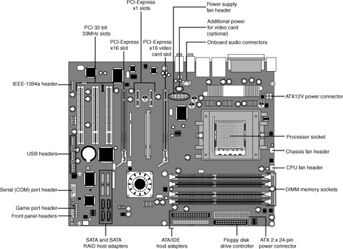
This section has figures and tables showing the configurations and pinouts of most of the other interface and I/O connectors you will find.
![]() See “AT/LPX Power Supply Connectors,” p. 937 (Chapter 18).
See “AT/LPX Power Supply Connectors,” p. 937 (Chapter 18).
![]() See “Serial Ports,” p. 791, and “Parallel Ports,” p. 795 (Chapter 14, “External I/O Interfaces”).
See “Serial Ports,” p. 791, and “Parallel Ports,” p. 795 (Chapter 14, “External I/O Interfaces”).
![]() See “Keyboard/Mouse Interface Connectors,” p. 814 (Chapter 15).
See “Keyboard/Mouse Interface Connectors,” p. 814 (Chapter 15).
![]() See “Universal Serial Bus (USB),” p. 766 (Chapter 14).
See “Universal Serial Bus (USB),” p. 766 (Chapter 14).
![]() See “An Overview of the IDE Interface,” p. 435 (Chapter 7, “The ATA/IDE Interface”).
See “An Overview of the IDE Interface,” p. 435 (Chapter 7, “The ATA/IDE Interface”).
One of the biggest problems many people overlook when building and upgrading systems is the front panel connections. Connectors that don’t match between the motherboard and chassis are one of the small but frustrating things that can be problematic in an otherwise smooth upgrade or system build. Having dependable standards for these connections would help, but unfortunately no official standard for the front panel connectors existed until October 2000, when Intel published the “Front Panel I/O Connectivity Design Guide.” The latest version of this guide can be found, along with the motherboard form factor specifications, at www.formfactors.org.
Before this standard was published, no official standard existed (and anarchy ruled). In addition, even though most chassis gave you individual tiny connectors for each function, some of the bigger system builders (for example, Dell, Gateway and others) began using specialized inline or dual-row header connectors so they could build systems more quickly and efficiently. Coincidentally, most of those vendors used Intel boards, hence Intel’s development of a standard.
The front panel guide details a 10-pin keyed header connector for the main front panel switch/LED functions, as well as a 10-pin keyed USB header, a 10-pin keyed IEEE 1394 (FireWire/i.LINK) header, a 10-pin keyed audio header, and a 6-pin keyed IR header. The pinouts and configurations of these and other motherboard-based connectors are shown in the following figures and tables. Figure 4.29 details the front panel switch/LED header connector.
Figure 4.29 Front panel switch/LED header connector.

The pinout of the standard front panel switch/LED connector is shown in Table 4.53.
Table 4.53 Front Panel Switch/LED Connector Pinout

Some chassis provide a single 10-pin header connector for the front panel switch/LED connections, but most provide individual 2-pin connectors for the various functions. If 2-pin connectors are used, they are connected as shown in Figure 4.30. Note that you can easily replace the multiple 2-pin connectors with a single 10-pin connector; some chassis even include an adapter for this purpose.
Figure 4.30 Standard front panel switch/LED connections using 2-pin connectors.
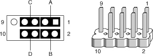
The 2-pin connections to a standard 10-pin front panel switch/LED connector are shown in Table 4.54.
Table 4.54 Front Panel Switch/LED Connections Using Multiple Connectors
A chassis can use either a single-color or dual-color LED for the Power LED function. A dual-color LED can provide more information about the various power and message states the system might be in, including power on/off, sleep, and message-waiting indications. Table 4.55 shows the possible states and meanings for both single- and dual-color power LEDs.
Table 4.55 Power LED Indications
Many motherboards do not follow the industry-standard guidelines for front panel switch/LED connections, and many use alternative designs instead, one of which is shown in Figure 4.31.
Figure 4.31 Alternative front panel switch/LED connector configuration.

Some of Intel’s older motherboards, as well as those made by other motherboard manufacturers, used a single-row pin header connector for the front panel connections, as shown in Figure 4.32.
Figure 4.32 Alternative single-row front panel connector configuration.
Table 4.56 shows the designations for the front panel motherboard connectors used on some motherboards.
Table 4.56 Alternative Single-Row Front Panel Connector Pinout
To adapt the connectors in your chassis to those on your motherboard, in some cases you might need to change the connector ends by removing the terminals and reinserting them into different positions. For example, I had a chassis that used a 3-pin power LED connection, whereas the motherboard only had a 2-pin connection. I had to remove one of the terminals, reinsert it into the middle position on the 3-pin connector, and then plug the connector into the motherboard so that two pins were mated and the third empty position was hanging off the end of the connector. Fortunately, the terminals are easy to remove by merely lifting a latch on the side of the connector and then sliding the terminal and wire back out. When the terminal is inserted, the latch automatically grabs the terminal and locks it into position.
Most motherboards include USB connectors, which are designed to be connected to front-mounted or rear bracket USB connectors in the chassis. The standard uses a single 10-pin keyed connector to provide two USB connections. The pinout of a standard dual USB motherboard header connector is shown in Figure 4.33 and Table 4.57.
Figure 4.33 Dual-USB header connector configuration.

Table 4.57 USB Header Connector Pinout

Many chassis includes multiple inline connectors for the dual USB–to–front panel or rear bracket connection, instead of a single keyed connector. An example of this is shown in Figure 4.34.
Figure 4.34 Front panel USB cable using multiple individual non-keyed connectors.

Using the multiple individual connectors shown in the previous figure, you would have to plug each individual connector into the proper pin. Some internal chassis USB cables use two 5-pin inline connectors, in which case you just need to ensure that you don’t put them on backward. Consult your motherboard and chassis manual for more information if you are unsure about your particular connections.
Caution
If your chassis uses multiple individual non-keyed connections, you must be sure to connect them properly to the connector on the motherboard. If you connect them improperly, you can cause a short circuit to occur that can damage the motherboard or any USB peripherals you plug into the front panel connectors. Higher-quality motherboards usually have self-healing fuses on the power signals, which can prevent damage if such a situation occurs.
Although IEEE 1394 (FireWire/i.LINK) is not found on most motherboards, some boards do incorporate this feature or offer it as an option. FireWire can also be added via an expansion card, and many of the cards have header connectors for front panel or rear bracket connections similar to that found on a motherboard. Figure 4.35 and Table 4.58 show the pinout of the industry-standard FireWire header connector.
Figure 4.35 IEEE 1394 (FireWire/i.LINK) header connector configuration.

Table 4.58 IEEE 1394 (FireWire/i.LINK) Connector Pinout
Note that the FireWire header connector has the same physical configuration and keying as a USB connector. This is unfortunate because it enables a USB front panel cable to be plugged into a FireWire connector, and vice versa. Either situation could cause a short circuit.
Caution
You must not plug a USB cable into a FireWire header connector, or a FireWire cable into a USB header connector. Doing so causes a short circuit that can damage the motherboard, as well as any peripherals you plug into the front panel connectors. Higher-quality motherboards usually have self-healing fuses on the power signals, which can prevent damage if such a situation occurs.
Motherboards that have integrated audio hardware usually feature a front panel audio header connector. The pinout of the industry-standard front panel audio header connector is shown in Figure 4.36 and Table 4.59.
Figure 4.36 Front panel audio header connector configuration.

Table 4.59 Front Panel Audio Connector Pinout

Some motherboards include an infrared data connector that connects to an infrared optical transceiver on the chassis front panel. This enables communication via infrared with cell phones, PDAs, laptops, printers, or other IrDA devices. The industry-standard pinout for IrDA connections on a motherboard is shown in Figure 4.37 and Table 4.60.
Figure 4.37 Infrared data front panel header connector configuration.

Table 4.60 Infrared Data Front Panel Connector Pinout

Other miscellaneous connectors might appear on motherboards as well; several are shown in Tables 4.61–4.69.
Table 4.62 LED and Keylock Connector
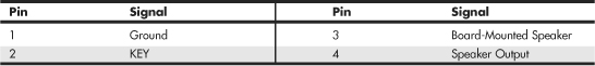
Table 4.64 Chassis Intrusion (Security) Pin-Header

Table 4.65 Wake on LAN Pin-Header
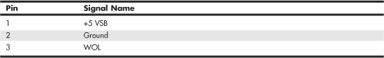
Table 4.66 Wake on Ring Pin-Header


Table 4.68 Telephony Connector

Table 4.69 ATAPI-Style Line In Connector
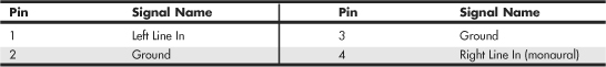
Note
Some boards have a board-mounted piezo speaker. It is enabled by placing a jumper over pins 3 and 4, which routes the speaker output to the board-mounted speaker. Removing the jumper enables a conventional speaker to be plugged in.
Most modern motherboards have three or four fan connectors for use with the processor fan, rear chassis fan, front chassis fan, and voltage regulator (power) fan (see Table 4.70). They all generally use the same 3-pin connector, with the third pin providing a tachometer signal for optional speed monitoring. If the motherboard is capable of monitoring the fan speed, it can sound an alarm when the fans begin to slow down due to bearing failure or wear. The alarm sound can vary, but it normally comes from the internal speaker and might be an ambulance siren–type sound.
Table 4.70 Fan Power Connectors

Caution
Do not place a jumper on this connector; serious board damage will result if the 12V is shorted to ground.
System Bus Types, Functions, and Features
The heart of any motherboard is the various buses that carry signals between the components. A bus is a common pathway across which data can travel within a computer. This pathway is used for communication and can be established between two or more computer elements.
The PC has a hierarchy of different buses. Most modern PCs have at least three buses; some have four or more. They are hierarchical because each slower bus is connected to the faster one above it. Each device in the system is connected to one of the buses, and some devices (primarily the chipset) act as bridges between the various buses.
The main buses in a modern system are as follows:
• Processor bus—Also called the front-side bus (FSB), this is the highest-speed bus in the system and is at the core of the chipset and motherboard. This bus is used primarily by the processor to pass information to and from cache or main memory and the North Bridge of the chipset. This is generally the fastest bus in the system, and the speed and width depends on the specific processor and chipset combination.
• AGP bus—This is a 32-bit bus designed specifically for a video card. It runs at 66MHz (AGP 1x), 133MHz (AGP 2x), 266MHz (AGP 4x), or 533MHz (AGP 8x), which allows for a bandwidth of up to 2,133MBps. It is connected to the North Bridge or Memory Controller Hub of the chipset and is manifested as a single AGP slot in systems that support it. Newer systems have phased out AGP slots in favor of PCI Express.
• PCI Express—The PCI Express bus is a third-generation development of the PCI bus that began to appear in mid-2004. PCI Express is a differential signaling bus that can be generated by either the North Bridge or South Bridge. The speed of PCI Express is described in terms of lanes. Each bidirectional dual-simplex lane provides a 2.5Gbps or 5Gbps transfer rate in each direction (250MBps or 500MBps effective speed). PCI Express video cards generally use the x16 slot, which provides 4,000MBps or 8,000MBps in each direction.
• PCI bus—This is usually a 33MHz 32-bit bus found in virtually all systems since the days of the Intel 486 CPU. Some newer systems include an optional 66MHz 64-bit version (mostly workstations or server-class systems). This bus is generated by either the chipset North Bridge in North/South Bridge chipsets or the I/O Controller Hub in chipsets using hub architecture. This bus is manifested in the system as a collection of 32-bit slots, normally white in color and numbering from four to six on most motherboards. Peripherals, such as SCSI adapters, network cards, video cards, and more, can be plugged into PCI bus slots. PCI Express is a faster development of the PCI bus.
• ISA bus—This is an 8MHz 16-bit bus that has disappeared from modern systems after first appearing in the original PC in 8-bit, 5MHz form and in the 1984 IBM AT in full 16-bit 8MHz form. It is a very slow-speed bus, but it was ideal for certain slow-speed or older peripherals. It has been used in the past for plug-in modems, sound cards, and various other low-speed peripherals. The ISA bus is created by the South Bridge part of the motherboard chipset, which acts as the ISA bus controller and the interface between the ISA bus and the faster PCI bus above it. The Super I/O chip usually was connected to the ISA bus on systems that included ISA slots.
Some motherboards feature a special connector called an Audio Modem Riser (AMR) or a Communications and Networking Riser (CNR). These are dedicated connectors for cards that are specific to the motherboard design to offer communications and networking options. They are not designed to be general-purpose bus interfaces, and few cards for these connectors are offered on the open market. Usually, they’re offered only as an option with a given motherboard. They are designed such that a motherboard manufacturer can easily offer its boards in versions with and without communications options, without having to reserve space on the board for optional chips. Normal network and modem options offered publicly, for the most part, are still PCI based because the AMR/CNR connection is somewhat motherboard specific. Figure 4.38 compares these connectors. Note that current motherboards have largely abandoned AMR and CNR slots.
Figure 4.38 The AMR slot (top left) and CNR slot (top center) compared to PCI slots. When the AMR slot is used, the PCI slot paired with it cannot be used.

Several hidden buses exist on modern motherboards—buses that don’t manifest themselves in visible slots or connectors. I’m talking about buses designed to interface chipset components, such as the Hub Interface and the LPC bus. The Hub Interface is a quad-clocked (4x) 66MHz 8-bit bus that carries data between the MCH and ICH in hub architecture chipsets made by Intel. It operates at a bandwidth of 266MBps and was designed as a chipset component connection that is faster than PCI and yet uses fewer signals for a lower-cost design. Some recent workstation/server chipsets and the latest 9xx-series desktop computer chipsets from Intel use faster versions of the hub interface. The most recent chipsets from major third-party vendors also bypass the PCI bus with direct high-speed connections between chipset components.
![]() See “High-speed North-South Bridge Connections,” p. 205 (this chapter).
See “High-speed North-South Bridge Connections,” p. 205 (this chapter).
In a similar fashion, the LPC bus is a 4-bit bus that has a maximum bandwidth of 16.67MBps; it was designed as an economical onboard replacement for the ISA bus. In systems that use LPC, it typically is used to connect Super I/O chip or motherboard ROM BIOS components to the main chipset. LPC is faster than ISA and yet uses far fewer pins and enables ISA to be eliminated from the board entirely.
The system chipset is the conductor that controls the orchestra of system components, enabling each to have its turn on its respective buses. Table 4.71 shows the widths, speeds, data cycles, and overall bandwidth of virtually all PC buses.
Table 4.71 Bandwidth (in MBps) and Detailed Comparison of Most PC Buses and Interfaces

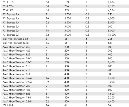


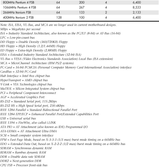
Note that many of the buses use multiple data cycles (transfers) per clock cycle to achieve greater performance. Therefore, the data transfer rate is higher than it would seem for a given clock rate, which allows for an easy way to take an existing bus and make it go faster in a backward-compatible way.
The Processor Bus (Front-Side Bus)
The processor bus (also called the front-side bus or FSB) is the communication pathway between the CPU and motherboard chipset—more specifically the North Bridge or Memory Controller Hub. This bus runs at the full motherboard speed—typically between 66MHz and 800MHz in modern systems, depending on the particular board and chipset design. This same bus also transfers data between the CPU and an external (L2) memory cache on Socket 7 (Pentium class) systems. Figure 4.39 shows how this bus fits into a typical Socket 7 PC system.
Figure 4.39 Typical Socket 7 (Pentium class) system architecture.
Figure 4.39 also shows where and how the other main buses, such as the PCI and ISA buses, fit into the system. As you can see, there is clearly a three-tier architecture with the fastest CPU bus on top, the PCI bus next, and the ISA bus at the bottom. Various components in the system are connected to one of these three main buses.
Socket 7 systems have an external (L2) cache for the CPU; the L2 cache is mounted on the motherboard and connected to the main processor bus that runs at the motherboard speed (usually between 66MHz and 100MHz). Thus, as the Socket 7 processors became available in faster and faster versions (through increasing the clock multiplier in the chip), the L2 cache unfortunately remained stuck on the motherboard running at the relatively slow (by comparison) motherboard speed. For example, the fastest Intel Socket 7 systems ran the CPU at 233MHz, which was 3.5 times the CPU bus speed of 66MHz. Therefore, the L2 cache ran at only 66MHz. The fastest Socket 7 systems used the AMD K6-2 550 processor, which ran at 550MHz—5.5 times a CPU bus speed of 100MHz. In those systems, the L2 cache ran at only 100MHz.
The problem of the slow L2 cache was first solved in the P6 class processors, such as the Pentium Pro, Pentium II, Celeron, Pentium III, and AMD Athlon and Duron. These processors used either Socket 8, Slot 1, Slot 2, Slot A, Socket A, or Socket 370. They moved the L2 cache off the motherboard and directly onto the CPU and connected it to the CPU via an on-chip back-side bus. Because the L2 cache bus was called the back-side bus, some in the industry began calling the main CPU bus the front-side bus. I still usually refer to it simply as the CPU bus.
With the L2 cache incorporated into the CPU, it can run at speeds up to the same as the processor itself. Most processors now incorporate the L2 cache directly on the CPU die, so the L2 cache runs at the same speed as the rest of the CPU. Others (mostly older versions) used separate dies for the cache integrated into the CPU package, which ran the L2 cache at some lower multiple (one-half, two-fifth, or one-third) of the main CPU. Even if the L2 ran at half or one-third of the processor speed, it still was significantly faster than the motherboard-bound cache on the Socket 7 systems.
In a Slot-1 type system the L2 cache is built into the CPU, but running at only half the processor speed. Slot A systems run the cache at one-half or one-third speed. The CPU bus speed increased from 66MHz (used primarily in Socket 7 systems) to 100MHz, enabling a bandwidth of 800MBps. Note that most of these systems included AGP support. Basic AGP was 66MHz (twice the speed of PCI), but most of these systems incorporated AGP 2x, which operated at twice the speed of standard AGP and enabled a bandwidth of 533MBps. These systems also typically used PC-100 SDRAM DIMMs, which have a bandwidth of 800MBps, matching the processor bus bandwidth for the best performance.
Slot 1 was dropped in favor of Socket 370 for the Pentium III and Celeron systems. This was mainly because these newer processors incorporated the L2 cache directly into the CPU die (running at the full-core speed of the processor) and an expensive cartridge with multiple chips was no longer necessary. At the same time, processor bus speeds increased to 133MHz, which enabled a throughput of 1,066MBps. Figure 4.40 shows a typical Socket 370 system design. AGP speed was also increased to AGP 4x, with a bandwidth of 1,066MBps.
Figure 4.40 Typical Socket 370 (Pentium III/Celeron class) system architecture.

Note the use of what Intel calls hub architecture instead of the older North/South Bridge design. This moves the main connection between the chipset components to a separate 266MBps hub interface (which has twice the throughput of PCI) and enables PCI devices to use the full bandwidth of PCI without fighting for bandwidth with a South Bridge. Also note that the flash ROM BIOS chip is now referred to as a Firmware Hub and is connected to the system via the LPC bus instead of via the Super I/O chip as in older North/South Bridge designs. The ISA bus is no longer used in most of these systems, and the Super I/O is connected via the LPC bus instead of ISA. The Super I/O chip also can easily be eliminated in these designs. This is commonly referred to as a legacy-free system because the ports supplied by the Super I/O chip are now known as legacy ports. Devices that would have used legacy ports would then be connected to the system via USB instead, and such systems would feature two USB controllers, with up to four total ports (more can be added by attaching USB hubs).
AMD processor systems adopted a Socket A design, which is similar to Socket 370 except it uses faster processor and memory buses. Although early versions retained the older North/South Bridge design, more recent versions use a design similar to Intel’s hub architecture. Note the high-speed CPU bus running up to 333MHz (2,667MBps throughput) and the use of DDR SDRAM DIMM modules that support a matching bandwidth of 2667MBps. It is always best for performance when the bandwidth of memory matches that of the processor. Finally, note how most of the South Bridge components include functions otherwise found in Super I/O chips; when these functions are included the chip is called a Super South Bridge.
The Pentium 4 uses a Socket 423 or Socket 478 design with hub architecture (see Figure 4.41). This design is most notable for including a 400MHz, 533MHz, or 800MHz CPU bus with a bandwidth of 3,200MBps, 4,266MBps, or 6,400MBps. The 533MHz and 800MHz models are currently faster than anything else on the market. In this example, note the use of dual-channel PC3200 (DDR400) SDRAM. A single PC-3200 DIMM has a bandwidth of 3,200MBps, but when running dual-channel (identical pairs of memory) mode, it has a bandwidth of 6,400MBps—which matches the bandwidth of the 800MHz CPU bus models of the Pentium 4 for best performance. Processors with the 533MHz CPU bus can use pairs of PC2100 (DDR266) or PC2700 (DDR333) memory modules in dual-channel mode to match the 4,266MBps throughput of this memory bus. It is always best when the throughput of the memory bus matches that of the processor bus.
Figure 4.41 Typical Socket 478 (Pentium 4) system architecture.

The Athlon 64 uses the high-speed HyperTransport architecture to connect the North Bridge or AGP Graphics Tunnel chip to the processor (Socket 754, 939, or 940). Most Athlon 64 chipsets use the 16-bit/800MHz version, but the latest chipsets designed for the new Socket 939 Athlon 64 FX-53 use the faster 16-bit/1GHz version to support faster DDR-2 memory.
However, the Athlon 64’s most significant departure from conventional computer architecture is the location of the memory controller. Rather than the memory controller being located in the North Bridge/MCH/GMCH chip, the Athlon 64/FX/Opteron architecture places it in the processor itself. This eliminates slow-downs caused by the use of an external memory controller and helps boost performance.
One drawback to the design, however, is that new memory technologies, such as DDR-2, require that the processor itself be redesigned.
Figure 4.42 illustrates an Athlon 64 FX-53–based system that uses the PCI Express x1 and PCI Express x16 expansion slot designs.
Figure 4.42 Typical Socket 939 (Athlon 64 FX-53) system architecture using PCI Express slots.
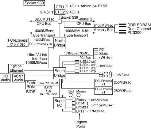
Calculating Processor Bus Speeds
Because the purpose of the processor bus is to get information to and from the CPU at the fastest possible speed, this bus typically operates at a rate faster than any other bus in the system. The bus consists of electrical circuits for data, addresses (the address bus, which is discussed in the following section), and control purposes. Most processors since the original Pentium have a 64-bit data bus, so they transfer 64 bits (8 bytes) at a time over the CPU bus.
The processor bus operates at the same base clock rate as the CPU does externally. This can be misleading because most CPUs these days run at a higher clock rate internally than they do externally. For example, an AMD Athlon 64 3800+ system has a processor running at 2.4GHz internally but only 400MHz externally, whereas a Pentium 4 3.4GHz runs at 3.4GHz internally but only 800MHz externally. In newer systems, the actual processor speed is some multiple (2x, 2.5x, 3x, and higher) of the processor bus.
![]() See “Comparing Processor Performance,” p. 49 (Chapter 3).
See “Comparing Processor Performance,” p. 49 (Chapter 3).
The processor bus is tied to the external processor pin connections and can transfer 1 bit of data per data line every cycle. Most modern processors transfer 64 bits (8 bytes) of data at a time.
To determine the transfer rate for the processor bus, you multiply the data width (64 bits or 8 bytes for a Celeron/Pentium III/4 or Athlon/Duron/Athlon XP/Athlon 64) by the clock speed of the bus (the same as the base or unmultiplied clock speed of the CPU).
For example, if you are using a Pentium 4 3.6GHz processor that runs on an 800MHz processor bus, you have a maximum instantaneous transfer rate of roughly 6,400MBps. You get this result by using the following formula:
800MHz × 8 bytes (64 bits) = 6,400MBps
With slower versions of the Pentium 4, you get either
533.33MHz × 8 bytes (64 bits) = 4,266MBps
or
400MHz × 8 bytes (64 bits) = 3,200MBps
With Socket A (Athlon XP), you get
333.33MHz × 8 bytes (64 bits) = 2,667MBps
or
266.66MHz × 8 bytes (64 bits) = 2,133MBps
or
200MHz × 8 bytes (64 bits) = 1,600MBps
With Socket 370 (Pentium III), you get
133.33MHz × 8 bytes (64 bits) = 1,066MBps
or
100MHz × 8 bytes (64 bits) = 800MBps
This transfer rate, often called the bandwidth of the processor bus, represents the maximum speed at which data can move. Refer to Table 4.71, later in this chapter, for a more complete list of various processor bus bandwidths.
Types of I/O Buses
Since the introduction of the first PC, many I/O buses have been introduced. The reason is simple: Faster I/O speeds are necessary for better system performance. This need for higher performance involves three main areas:
• Faster CPUs
• Increasing software demands
• Greater multimedia requirements
Each of these areas requires the I/O bus to be as fast as possible.
One of the primary reasons new I/O bus structures have been slow in coming is compatibility—that old catch-22 that anchors much of the PC industry to the past. One of the hallmarks of the PC’s success is its standardization. This standardization spawned thousands of third-party I/O cards, each originally built for the early bus specifications of the PC. If a new high-performance bus system was introduced, it often had to be compatible with the older bus systems so the older I/O cards would not be obsolete. Therefore, bus technologies seem to evolve rather than make quantum leaps forward.
You can identify different types of I/O buses by their architectures. The main types of I/O buses are detailed earlier in this chapter.
The main differences among buses consist primarily of the amounts of data they can transfer at one time and the speeds at which they can do it. The following sections describe the various types of PC buses.
The ISA Bus
Industry Standard Architecture (ISA) is the bus architecture that was introduced as an 8-bit bus with the original IBM PC in 1981; it was later expanded to 16 bits with the IBM PC/AT in 1984. ISA is the basis of the modern personal computer and was the primary architecture used in the vast majority of PC systems until the late 1990s. It might seem amazing that such a presumably antiquated architecture was used for so long, but it provided reliability, affordability, and compatibility, plus this old bus is still faster than many of the peripherals we connect to it!
Note
The ISA bus has vanished from all recent desktop systems, and few companies make or sell ISA cards anymore. The ISA bus continues to be popular with industrial computer (PICMG) designs, but it is expected to eventually fade away from these as well.
Two versions of the ISA bus exist, based on the number of data bits that can be transferred on the bus at a time. The older version is an 8-bit bus; the newer version is a 16-bit bus. The original 8-bit version ran at 4.77MHz in the PC and XT, and the 16-bit version used in the AT ran at 6MHz and then 8MHz. Later, the industry as a whole agreed on an 8.33MHz maximum standard speed for 8/16-bit versions of the ISA bus for backward compatibility. Some systems have the capability to run the ISA bus faster than this, but some adapter cards will not function properly at higher speeds. ISA data transfers require anywhere from two to eight cycles. Therefore, the theoretical maximum data rate of the ISA bus is about 8MBps, as the following formula shows:
8.33MHz × 2 bytes (16 bits) ÷ 2 cycles per transfer = 8.33MBps
The bandwidth of the 8-bit bus would be half this figure (4.17MBps). Remember, however, that these figures are theoretical maximums. Because of I/O bus protocols, the effective bandwidth is much lower—typically by almost half. Even so, at about 8MBps, the ISA bus is still faster than many of the peripherals connected to it, such as serial ports, parallel ports, floppy controllers, keyboard controllers, and so on.
The 8-Bit ISA Bus
This bus architecture is used in the original IBM PC computers and was retained for several years in later systems. Although virtually nonexistent in new systems today, this architecture still exists in hundreds of thousands of PC systems in the field, including systems with 286 and 386 processors.
Physically, the 8-bit ISA expansion slot resembles the tongue-and-groove system furniture makers once used to hold two pieces of wood together. It is specifically called a card/edge connector. An adapter card with 62 contacts on its bottom edge plugs into a slot on the motherboard that has 62 matching contacts. Electronically, this slot provides eight data lines and 20 addressing lines, enabling the slot to handle 1MB of memory.
Figure 4.43 describes the pinouts for the 8-bit ISA bus; Figure 4.44 shows how these pins are oriented in the expansion slot.
Figure 4.43 Pinouts for the 8-bit ISA bus.

Figure 4.44 The 8-bit ISA bus connector.
Although the design of the bus is simple, IBM waited until 1987 to publish full specifications for the timings of the data and address lines, so in the early days of PC compatibles, manufacturers had to do their best to figure out how to make adapter boards. This problem was solved, however, as PC-compatible personal computers became more widely accepted as the industry standard and manufacturers had more time and incentive to build adapter boards that worked correctly with the bus.
The dimensions of 8-bit ISA adapter cards are as follows:
4.2″ (106.68mm) high
13.13″ (333.5mm) long
0.5″ (12.7mm) wide
The 16-Bit ISA Bus
IBM threw a bombshell on the PC world when it introduced the AT with the 286 processor in 1984. This processor had a 16-bit data bus, which meant communications between the processor and motherboard as well as memory would now be 16 bits wide instead of only 8. Although this processor could have been installed on a motherboard with only an 8-bit I/O bus, that would have meant a huge sacrifice in the performance of any adapter cards or other devices installed on the bus.
Rather than create a new I/O bus, at that time IBM instead came up with a system that could support both 8- and 16-bit cards by retaining the same basic 8-bit connector layout but adding an optional 16-bit extension connector. This first debuted on the PC/AT in August 1984, which is why we also refer to the ISA bus as the AT-bus.
The extension connector in each 16-bit expansion slot adds 36 connector pins (for a total of 98 signals) to carry the extra signals necessary to implement the wider data path. In addition, two of the pins in the 8-bit portion of the connector were changed. These two minor changes did not alter the function of 8-bit cards.
Figure 4.45 describes the pinouts for the full 16-bit ISA expansion slot, and Figure 4.46 shows how the additional pins are oriented in the expansion slot.
Figure 4.45 Pinouts for the 16-bit ISA bus.

Figure 4.46 The ISA 16-bit bus connector.
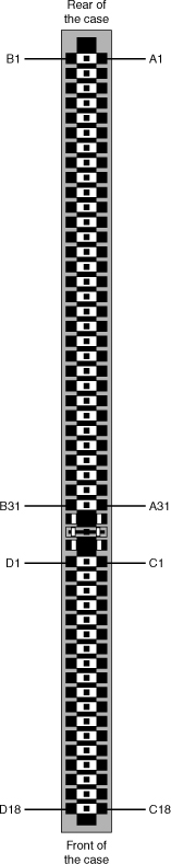
Because of physical interference with some ancient 8-bit card designs, IBM left 16-bit extension connectors off two of the slots in the AT. This was not a problem in newer systems, so any system with ISA slots would have all of them as full 16-bit versions.
The dimensions of a typical AT expansion board are as follows:
4.8″ (121.92mm) high
13.13″ (333.5mm) long
0.5″ (12.7mm) wide
Two heights actually are available for cards commonly used in AT systems: 4.8″ and 4.2″ (the height of older PC-XT cards). The shorter cards became an issue when IBM introduced the XT Model 286. Because this model has an AT motherboard in an XT case, it needs AT-type boards with the 4.2″ maximum height. Most board makers trimmed the height of their boards; most manufacturers who still make ISA cards now make only 4.2″-tall (or less) boards so they will work in systems with either profile.
32-Bit Buses
After 32-bit CPUs became available, it was some time before 32-bit bus standards became available. Before MCA and EISA specs were released, some vendors began creating their own proprietary 32-bit buses, which were extensions of the ISA bus. Fortunately, these proprietary buses were few and far between.
The expanded portions of the bus typically are used for proprietary memory expansion or video cards. Because the systems are proprietary (meaning that they are nonstandard), pinouts and specifications are not available.
The Micro Channel Bus
The introduction of 32-bit chips meant that the ISA bus could not handle the power of another new generation of CPUs. The chips could transfer 32 bits of data at a time, but the ISA bus can handle a maximum of only 16 bits. Rather than extend the ISA bus again, IBM decided to build a new bus; the result was the MCA bus. MCA (an abbreviation for microchannel architecture) is completely different from the ISA bus and is technically superior in every way.
IBM wanted not only to replace the old ISA standard, but also to require vendors to license certain parts of the technology. Many owed for licenses on the ISA bus technology that IBM also created, but because IBM had not been aggressive in its licensing of ISA, many got away without any license. Problems with licensing and control led to the development of the competing EISA bus (see the next section on the EISA bus) and hindered acceptance of the MCA bus.
MCA systems produced a new level of ease of use; they were plug-and-play before the official Plug and Play specification even existed. An MCA system had no jumpers and switches—neither on the motherboard nor on any expansion adapter. Instead you used a special Reference disk, which went with the particular system, and Option disks, which went with each of the cards installed in the system. After a card was installed, you loaded the Option disk files onto the Reference disk; after that, you didn’t need the Option disks anymore. The Reference disk contained the special BIOS and system setup program necessary for an MCA system, and the system couldn’t be configured without it.
For more information on the MCA bus, see the previous editions of this book on the included disc.
The EISA Bus
The Extended Industry Standard Architecture (EISA) standard was announced in September 1988 as a response to IBM’s introduction of the MCA bus—more specifically, to the way IBM wanted to handle licensing of the MCA bus. Vendors did not feel obligated to pay retroactive royalties on the ISA bus, so they turned their backs on IBM and created their own buses.
The EISA standard was developed primarily by Compaq and was intended to be its way of taking over future development of the PC bus from IBM. Compaq knew that nobody would clone its bus if it was the only company that had it, so it essentially gave the design to other leading manufacturers. Compaq formed the EISA committee, a nonprofit organization designed specifically to control development of the EISA bus. Very few EISA adapters were ever developed. Those that were developed centered mainly around disk array controllers and server-type network cards.
The EISA bus was essentially a 32-bit version of ISA. Unlike the MCA bus from IBM, you could still use older 8-bit or 16-bit ISA cards in 32-bit EISA slots, providing for full backward compatibility. As with MCA, EISA also allowed for automatic configuration of EISA cards via software.
The EISA bus added 90 new connections (55 new signals plus grounds) without increasing the physical connector size of the 16-bit ISA bus. At first glance, the 32-bit EISA slot looks a lot like the 16-bit ISA slot. The EISA adapter, however, has two rows of stacked contacts. The first row is the same type used in 16-bit ISA cards; the other, thinner row extends from the 16-bit connectors. Therefore, ISA cards can still be used in EISA bus slots. Although this compatibility was not enough to ensure the popularity of EISA buses, it is a feature that was carried over into the VL-Bus standard that followed. The physical specifications of an EISA card are as follows:
• 5″ (127mm) high
• 13.13″ (333.5mm) long
• 0.5″ (12.7mm) wide
The EISA bus can handle up to 32 bits of data at an 8.33MHz cycle rate. Most data transfers require a minimum of two cycles, although faster cycle rates are possible if an adapter card provides tight timing specifications. The maximum bandwidth on the bus is 33MBps, as the following formula shows:
8.33MHz × 4 bytes (32 bits) = 33MBps
Local Buses (VESA, PCI, PCI Express, AGP)
The I/O buses discussed so far (ISA, MCA, and EISA) have one thing in common: relatively slow speed. The next three bus types that are discussed in the following few sections all use the local bus concept explained in this section to address the speed issue. The main local buses found in PC systems are
• PCI
• AGP
The speed limitation of ISA, MCA, and EISA is a carryover from the days of the original PC when the I/O bus operated at the same speed as the processor bus. As the speed of the processor bus increased, the I/O bus realized only nominal speed improvements, primarily from an increase in the bandwidth of the bus. The I/O bus had to remain at a slower speed because the huge installed base of adapter cards could operate only at slower speeds.
A local bus is any bus designed to interact more closely with the processor, or closer to processor throughput. It is interesting to note that the very first 8-bit and 16-bit ISA buses were a form of local bus architecture. These systems had the processor bus as the main bus, and everything ran at full processor speeds. When ISA systems ran faster than 8MHz, the main ISA bus had to be decoupled from the processor bus because expansion cards, memory, and so on could not keep up. In 1992, an extension to the ISA bus called the VESA local bus (VL-Bus) started showing up on PC systems, indicating a return to local bus architecture. Since then, the peripheral component interconnect (PCI) Express local bus has supplanted other popular bus architectures as the most common high-speed connection for devices in a PC.
Local bus solutions do not necessarily replace earlier standards, such as ISA; they are designed into the system as a bus that is closer to the processor in the system architecture. Older buses such as ISA were kept around for backward compatibility with slower types of adapters that didn’t need any faster connection to the system (such as modems). Therefore, a typical system might have several different types of slots, including PCI Express, PCI, AGP, and/or ISA slots.
VESA Local Bus
The Video Electronics Standards Association (VESA) local bus was the most popular local bus design from its debut in August 1992 through 1994. It was created by the VESA committee, a nonprofit organization originally founded by NEC to further develop video display and bus standards. In a similar fashion to how EISA evolved, NEC had done most of the work on the VL-Bus (as it would be called) and, after founding the nonprofit VESA committee, NEC turned over future development to VESA. At first, the local bus slot seemed designed to be used primarily for video cards. Improving video performance was a top priority at NEC to help sell its high-end displays as well as its own PC systems. By 1991, video performance had become a real bottleneck in most PC systems.
The VL-Bus can move data 32 bits at a time, enabling data to flow between the CPU and a compatible video subsystem or hard drive at the full 32-bit data width of the 486 chip. The maximum rated throughput of the VL-Bus is 133MBps. In other words, local bus went a long way toward removing the major bottlenecks that existed in earlier bus configurations.
Unfortunately, the VL-Bus did not seem to be a long-lived concept. The design was simple indeed—just take the pins from the 486 processor and run them out to a card connector socket. So, the VL-Bus is essentially the raw 486 processor bus. This allowed for a very inexpensive design because no additional chipsets or interface chips were required. A motherboard designer could add VL-Bus slots to its 486 motherboards very easily and at a very low cost. This is why these slots appeared on virtually all 486 system designs overnight.
Problems arose with timing glitches caused by the capacitance introduced into the circuit by different cards. Because the VL-Bus ran at the same speed as the processor bus, different processor speeds meant different bus speeds, and full compatibility was difficult to achieve. Although the VL-Bus could be adapted to other processors—including the 386 or even the Pentium—it was designed for the 486 and worked best as a 486 solution only. Despite the low cost, after a new bus called PCI appeared, VL-Bus fell into disfavor very quickly. It never did catch on with Pentium systems, and there was little or no further development of the VL-Bus in the PC industry.
Physically, the VL-Bus slot was an extension of the slots used for whatever type of base system you have. If you have an ISA system, the VL-Bus is positioned as an extension of your existing 16-bit ISA slots. The VESA extension has 112 contacts and uses the same physical connector as the MCA bus.
The PCI Bus
In early 1992, Intel spearheaded the creation of another industry group. It was formed with the same goals as the VESA group in relation to the PC bus. Recognizing the need to overcome weaknesses in the ISA and EISA buses, the PCI Special Interest Group was formed.
The PCI bus specification was released in June 1992 as version 1.0 and since then has undergone several upgrades. Table 4.72 shows the various releases of PCI.

PCI redesigned the traditional PC bus by inserting another bus between the CPU and the native I/O bus by means of bridges. Rather than tap directly into the processor bus, with its delicate electrical timing (as was done in the VL-Bus), a new set of controller chips was developed to extend the bus, as shown in Figure 4.47.
Figure 4.47 Conceptual diagram of the PCI bus.
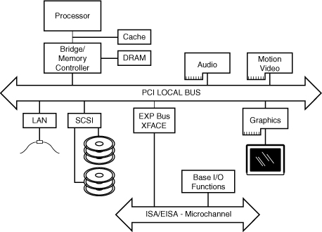
The PCI bus often is called a mezzanine bus because it adds another layer to the traditional bus configuration. PCI bypasses the standard I/O bus; it uses the system bus to increase the bus clock speed and take full advantage of the CPU’s data path. Systems that integrate the PCI bus became available in mid-1993 and have since become a mainstay in the PC.
Information typically is transferred across the PCI bus at 33MHz and 32 bits at a time. The bandwidth is 133MBps, as the following formula shows:
33.33MHz × 4 bytes (32 bits) = 133MBps
Although 32-bit 33MHz PCI is the standard found in most PCs, there are now several variations on PCI, as shown in Table 4.73. Most recent PCs now also feature PCI Express x1 and PCI Express x16 slots.

Currently, the 64-bit or 66MHz and 133MHz variations are used only on server- or workstation-type boards and systems. Aiding performance is the fact that the PCI bus can operate concurrently with the processor bus; it does not supplant it. The CPU can be processing data in an external cache while the PCI bus is busy transferring information between other parts of the system—a major design benefit of the PCI bus.
A PCI adapter card uses its own unique connector. This connector can be identified within a computer system because it typically is offset from the normal ISA, MCA, or EISA connectors found in older motherboards. See Figure 4.48 for an example. The size of a PCI card can be the same as that of the cards used in the system’s normal I/O bus.
Figure 4.48 Typical configuration of 32-bit 33MHz PCI slots in relation to ISA or EISA and AGP slots.
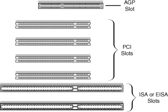
The PCI specification identifies three board configurations, each designed for a specific type of system with specific power requirements; each specification has a 32-bit version and a longer 64-bit version. The 5V specification is for stationary computer systems (using PCI 2.2 or earlier versions), the 3.3V specification is for portable systems (also supported by PCI 2.3), and the universal specification is for motherboards and cards that work in either type of system. 64-bit versions of the 5V and universal PCI slots are found primarily on server motherboards. The PCI-X 2.0 specifications for 266 and 533 versions support 3.3V and 1.5V signaling; this corresponds to PCI version 2.3, which supports 3.3V signaling.
Note
The pinouts for the 5V, 3.3V, and universal PCI slots can be found on the disc in the Technical Reference section.
Figure 4.49 compares the 32-bit and 64-bit versions of the standard 5V PCI slot to a 64-bit universal PCI slot. Figure 4.50 shows how the connector on a 64-bit universal PCI card compares to the 64-bit universal PCI slot.
Figure 4.49 A 32-bit 33MHz PCI slot (top) compared to a 64-bit 33MHz PCI slot (center) and a 64-bit universal PCI slot that runs at 66MHz (bottom).
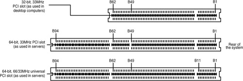
Figure 4.50 A 64-bit universal PCI card (top) compared to the 64-bit universal PCI slot (bottom).

Notice that the universal PCI board specifications effectively combine the 5V and 3.3V specifications. For pins for which the voltage is different, the universal specification labels the pin V I/O. This type of pin represents a special power pin for defining and driving the PCI signaling rail.
Another important feature of PCI is the fact that it was the model for the Intel PnP specification. Therefore, PCI cards do not have jumpers and switches and are instead configured through software. True PnP systems are capable of automatically configuring the adapters, whereas non-PnP systems with ISA slots must configure the adapters through a program that is usually a part of the system CMOS configuration. Starting in late 1995, most PC-compatible systems have included a PnP BIOS that allows the automatic PnP configuration.
PCI Express
During 2001, a group of companies called the Arapahoe Work Group (led primarily by Intel) developed a draft of a new high-speed bus specification code-named 3GIO (third-generation I/O). In August 2001, the PCI Special Interest Group (PCI-SIG) agreed to take over, manage, and promote the 3GIO architecture specification as the future generation of PCI. In April 2002, the 3GIO draft version 1.0 was completed, transferred to the PCI-SIG, and renamed PCI Express. Finally in July 2002, the PCI Express 1.0 specification was approved. The specification was updated to 1.1 in April 2005, and 2.0 in January 2007.
The original 3GIO code name was derived from the fact that this new bus specification was designed to initially augment and eventually replace the previously existing ISA/AT-Bus (first-generation) and PCI (second-generation) bus architectures in PCs. Each of the first two generations of PC bus architectures was designed to have a 10-to-15-year useful life in PCs. In being adopted and approved by the PCI-SIG, PCI Express is now destined to be the dominant PC bus architecture designed to support the increasing bandwidth needs in PCs over the next 10–15 years.
The key features of PCI Express are as follows:
• Compatibility with existing PCI enumeration and software device drivers.
• Physical connection over copper, optical, or other physical media to allow for future encoding schemes.
• Maximum bandwidth per pin allows for small form factors, reduced cost, simpler board designs and routing, and reduced signal integrity issues.
• Embedded clocking scheme enables easy frequency (speed) changes as compared to synchronous clocking.
• Bandwidth (throughput) increases easily with frequency and width (lane) increases.
• Low latency suitable for applications requiring isochronous (time-sensitive) data delivery, such as streaming video.
• Hot-plugging and hot-swapping capabilities.
• Power management capabilities.
PCI Express is another example of how the PC is moving from parallel to serial interfaces. Earlier generation bus architectures in the PC have been of a parallel design, in which multiple bits are sent simultaneously over several pins in parallel. The more bits sent at a time, the faster the bus throughput is. The timing of all the parallel signals must be the same, which becomes more and more difficult to do over faster and longer connections. Even though 32 bits can be transmitted simultaneously over a bus such as PCI or AGP, propagation delays and other problems cause them to arrive slightly skewed at the other end, resulting in a time difference between when the first and last of all the bits arrive.
A serial bus design is much simpler, sending 1 bit at a time over a single wire, at much higher rates of speed than a parallel bus would allow. By sending the bits serially, the timing of individual bits or the length of the bus becomes much less of a factor. By combining multiple serial data paths, even faster throughputs can be realized that dramatically exceed the capabilities of traditional parallel buses.
PCI Express is a very fast serial bus design that is backward compatible with current PCI parallel bus software drivers and controls. In PCI Express, data is sent full duplex (simultaneously operating one-way paths) over two pairs of differentially signaled wires called a lane. Each lane allows for about 250MBps throughput in each direction initially, and the design allows for scaling from 1 to 2, 4, 8, 16, or 32 lanes. For example, a high-bandwidth configuration with 16 lanes allowing 16 bits to be sent in each direction simultaneously would allow up to 4,000MBps bandwidth each way. PCIe 2.0 increases the transfer rate to 500MBps per lane, or 8,000MBps for an x16 connector. This compares to PCI, which has only 133MBps bandwidth (one way at a time). Figure 4.51 compares the PCI Express x1–x16 connectors. Note that the PCI Express x4 and x8 connectors shown in this figure are intended primarily for use in servers.
Figure 4.51 PCI Express x1, x4, x8, and x16 slots.
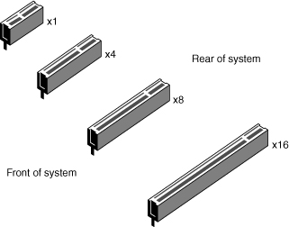
PCI Express uses an IBM-designed 8-bit-to-10-bit encoding scheme, which allows for self-clocked signals that will easily allow future increases in frequency. The starting frequency is 2.5GHz, and the specification will allow increasing up to 10GHz in the future, which is about the limit of copper connections. By combining frequency increases with the capability to use up to 32 lanes, PCI Express will be capable of supporting future bandwidths up to 32GBps.
PCI Express is designed to augment and eventually replace many of the buses currently used in PCs. It will not only be a supplement to (and the eventual replacement for) PCI slots, but can also be used to replace the existing Intel hub architecture, HyperTransport, and similar high-speed interfaces between motherboard chipset components. Additionally, it will replace video interfaces such as AGP and act as a mezzanine bus to attach other interfaces, such as Serial ATA, USB 2.0, 1394b (FireWire or i.LINK), Gigabit Ethernet, and more.
Because PCI Express can be implemented over cables as well as onboard, it can be used to create systems constructed with remote “bricks” containing the bulk of the computing power. Imagine the motherboard, processor, and RAM in one small box hidden under a table, with the video, disk drives, and I/O ports in another box sitting out on a table within easy reach. This will enable a variety of flexible PC form factors to be developed in the future without compromising performance.
PCI Express has not and will not replace PCI or other interfaces overnight. System developers will continue to integrate PCI, AGP, and other bus architectures into system designs for several more years. Just as with PCI and the ISA/AT-Bus before, there will likely be a long period of time during which both buses will be found on motherboards. Gradually, though, fewer PCI and more PCI Express connections will appear. Over time, PCI Express will eventually become the preferred general-purpose I/O interconnect over PCI. I expect the move to PCI Express will be similar to the transition from ISA/AT-Bus to PCI during the 1990s. Current full-size ATX motherboards have about half their slots as PCI and half as PCI Express.
Although it will take some time for PCI Express to completely replace PCI, PCI Express x16 has already replaced AGP 8x.
Most recent desktop motherboard designs feature a mix of PCI, PCI Express x1, and x16 slots; workstation and server motherboards are also adding PCI Express slots to their typical PCI-X and PCI slots.
For more information on PCI Express, I recommend consulting the PCI-SIG website (www.pcisig.org).
Accelerated Graphics Port
In the mid 1990s Intel created AGP as a new bus specifically designed for high-performance graphics and video support. AGP is based on PCI, but it contains several additions and enhancements and is physically, electrically, and logically independent of PCI. For example, the AGP connector is similar to PCI, although it has additional signals and is positioned differently in the system. Unlike PCI, which is a true bus with multiple connectors (slots), AGP is more of a point-to-point high-performance connection designed specifically for a video card in a system because only one AGP slot is allowed for a single video card. Intel originally released the AGP specification 1.0 in July 1996 and defined a 66MHz clock rate with 1x or 2x signaling using 3.3V. AGP version 2.0 was released in May 1998 and added 4x signaling as well as a lower 1.5V operating capability.
The final revision for the AGP specification for PCs is AGP 8x, also called AGP 3.0. AGP 8x defines a transfer speed of 2,133MBps, which is twice that of AGP 4x. The AGP 8x specification was first publicly announced in November 2000. AGP 8x support is now widely available in motherboard chipsets and graphics chipsets from major vendors. Although AGP 8x has a maximum speed twice that of AGP 4x, the real-world differences between AGP 4x- and 8x-compatible devices with otherwise identical specifications are minimal. However, many 3D chipsets that support AGP 8x have also upgraded memory and 3D graphics core speeds and designs to better support the faster interface.
Most of the last generation of AGP video cards are designed to conform to the AGP 4X or AGP 8X specification, each of which runs on only 1.5 volts. Most older motherboards with AGP 2X slots are designed to accept only 3.3V cards. If you plug a 1.5V card into a 3.3V slot, both the card and motherboard could be damaged, so special keys have been incorporated into the AGP specification to prevent such disasters. Normally, the slots and cards are keyed such that 1.5V cards fit only in 1.5V sockets and 3.3V cards fit only in 3.3V sockets. However, universal sockets do exist that accept either 1.5V or 3.3V cards. The keying for the AGP cards and connectors is dictated by the AGP standard, as shown in Figure 4.52.
Figure 4.52 AGP 4x/8x (1.5V) card and AGP 3.3V, universal, and 1.5V slots.

As you can see from Figure 4.60, AGP 4x or 8x (1.5V) cards fit only in 1.5V or universal (3.3V or 1.5V) slots. Due to the design of the connector and card keys, a 1.5V card cannot be inserted into a 3.3V slot. So, if your new AGP card won’t fit in the AGP slot in your existing motherboard, consider that a good thing because if you were able to plug it in, you would fry the card and possibly the board as well! In that case, you’d either have to return the 4x/8x card or get a new motherboard that supports the 4x/8x (1.5V) cards.
Caution
Some AGP 4x/8x-compatible motherboards require you to use 1.5V AGP 4x/8x cards only; be sure to check compatibility between the motherboard and the AGP card you want to buy to avoid problems. Some AGP 4x/8x-compatible slots use the card retention mechanism shown in Figure 4.60. Note that AGP 1x/2x slots have a visible divider not present on the newer AGP 4x slot. AGP 4x slots can also accept AGP 8x cards, and vice versa.
Additionally, a newer specification was introduced as AGP Pro 1.0 in August 1998 and was revised in April 1999 as AGP Pro 1.1a. It defines a slightly longer slot with additional power pins at each end to drive bigger and faster AGP cards that consume more than 25 watts of power, up to a maximum of 110 watts. AGP Pro cards are likely to be used for high-end graphics workstations and are not likely to be found in any normal PCs. However, AGP Pro slots are backward compatible, meaning a standard AGP card will plug in, and a number of motherboard vendors began using AGP Pro slots rather than AGP 4x slots in their products. Because AGP Pro slots are longer, an AGP 1x/2x card can be incorrectly inserted into the slot, which could damage it, so some vendors supply a cover or an insert for the AGP Pro extension at the rear of the slot. This protective cover or insert should be removed only if you want to install an AGP Pro card.
The standard AGP 1x/2x, AGP 4x, and AGP Pro slots are compared to each other in Figure 4.53.
Figure 4.53 AGP standard (1x/2x), AGP 4x, and AGP Pro slots compared to each other. AGP 4x and AGP Pro can accept AGP 1x, 2x, and 4x cards. AGP 4x and AGP Pro slots can also accept AGP 8x cards.

AGP runs at a base frequency of 66MHz (actually 66.66MHz), which is double that of standard PCI. In the basic AGP mode, called 1x, a single transfer is done every cycle. Because the AGP bus is 32 bits (4 bytes) wide, at 66 million times per second it would be capable of transferring data at a rate of about 266MBps! The original AGP specification also defines a 2x mode, in which two transfers are performed every cycle, resulting in 533MBps. Using an analogy in which every cycle is equivalent to the back-and-forth swing of a pendulum, the 1x mode is thought of as transferring information at the start of each swing. In 2x mode, an additional transfer would occur every time the pendulum completed half a swing, thereby doubling performance while technically maintaining the same clock rate, or in this case, the same number of swings per second. Although the earliest AGP cards supported only the AGP 1x mode, most vendors quickly shifted to the AGP 2x mode. The newer AGP 2.0 specification adds the capability for 4x transfers, in which data is transferred four times per cycle and equals a data transfer rate of 1,066MBps. Most current AGP cards have support for the 4x standard as a minimum, and many graphics chipsets from NVIDIA and ATI support AGP 8x. Table 4.74 shows the differences in clock rates and data transfer speeds (bandwidth) for the various AGP modes.
Table 4.74 AGP Modes Showing Clock Speeds and Bandwidth

Because AGP is independent of PCI, using an AGP video card frees up the PCI bus for more traditional input and output, such as for IDE/ATA or SCSI controllers, USB controllers, sound cards, and so on.
Besides faster video performance, one of the main reasons Intel designed AGP was to allow the video card to have a high-speed connection directly to the system RAM, which would enable a reasonably fast and powerful video solution to be integrated at a lower cost. AGP allows a video card to have direct access to the system RAM, either enabling lower-cost video solutions to be directly built into a motherboard without having to include additional video RAM or enabling an AGP card to share the main system memory. However, few AGP cards in recent years share main memory. Instead, they have their own high-speed memory (as much as 256MB in some recent models). Using dedicated memory directly on the video card is especially important when running high-performance 3D video applications. AGP enables the speed of the video card to pace the requirements for high-speed 3D graphics rendering as well as full-motion video on the PC.
Although AGP 8x (2,133MBps) is 16 times faster than 32-bit 33MHz PCI (133MBps), AGP 8x is only about half as fast as PCI Express x16 (4,000MBps). Starting in mid-2004, motherboard and system vendors began to replace AGP 8x with PCI Express x16 expansion slots in high-performance systems. By early 2006, most motherboards featured PCI Express x16 slots in place of AGP.
System Resources
System resources are the communications channels, addresses, and other signals hardware devices use to communicate on the bus. At their lowest level, these resources typically include the following:
• Memory addresses
• IRQ (interrupt request) channels
• DMA (direct memory access) channels
• I/O port addresses
These resources are required and used by many components of your system. Adapter cards need these resources to communicate with your system and accomplish their purposes. Not all adapter cards have the same resource requirements. A serial communications port, for example, needs an IRQ channel and I/O port address, whereas a sound card needs these resources and at least one DMA channel.
As systems have increased in complexity, the chance for resource conflicts also increased. The configuration problem came to a head in the early 1990s, when manual configuration was the norm. Starting around that time, Microsoft and Intel developed a technology called Plug and Play (PnP), which allowed for automatic detection, management and configuration of hardware, most times without any user involvement. Windows 95 was the first PnP aware PC operating system, and by the time it was released, most hardware began supporting the PnP standard. Plug and Play was later superceded by ACPI (Advanced Configuration and Power Interface), which combined device configuration and power management into a single specification.
Modern systems with ACPI and modern buses such as PCI and PCI Express rarely have problems configuring these resources. In virtually all cases the configuration will be automatic and trouble free.
Interrupts
Interrupt request channels, or hardware interrupts, are used by various hardware devices to signal the motherboard that a request must be fulfilled. This procedure is the same as a student raising his hand to indicate that he needs attention.
These interrupt channels are represented by wires on the motherboard and in the slot connectors. When a particular interrupt is invoked, a special routine takes over the system, which first saves all the CPU register contents in a stack and then directs the system to the interrupt vector table. This vector table contains a list of memory addresses that correspond to the interrupt channels. Depending on which interrupt was invoked, the program corresponding to that channel is run.
The pointers in the vector table point to the address of whatever software driver is used to service the card that generated the interrupt. For a network card, for example, the vector might point to the address of the network drivers that have been loaded to operate the card; for a hard disk controller, the vector might point to the BIOS code that operates the controller.
After the particular software routine finishes performing whatever function the card needed, the interrupt-control software returns the stack contents to the CPU registers, and the system then resumes whatever it was doing before the interrupt occurred.
Through the use of interrupts, your system can respond to external events in a timely fashion. Each time a serial port presents a byte to your system, an interrupt is generated to ensure that the system reads that byte before another comes in. Keep in mind that in some cases a port device—in particular, a modem with a 16550 or higher UART chip—might incorporate a byte buffer that allows multiple characters to be stored before an interrupt is generated.
Hardware interrupts are generally prioritized by their numbers; with some exceptions, the highest-priority interrupts have the lowest numbers. Higher-priority interrupts take precedence over lower-priority interrupts by interrupting them. As a result, several interrupts can occur in your system concurrently, with each interrupt nesting within another.
The ISA bus uses edge-triggered interrupt sensing, in which an interrupt is sensed by a changing signal sent on a particular wire located in the slot connector. A different wire corresponds to each possible hardware interrupt. Because the motherboard can’t recognize which slot contains the card that used an interrupt line and therefore generated the interrupt, confusion results if more than one card is set to use a particular interrupt. Each interrupt, therefore, is usually designated for a single hardware device. Most of the time, interrupts can’t be shared.
Originally, IBM developed ways to share interrupts on the ISA bus, but few devices followed the necessary rules to make this a reality. The PCI bus inherently allows interrupt sharing; in fact, virtually all PCI cards are set to PCI interrupt A and share that interrupt on the PCI bus. The real problem is that there are technically two sets of hardware interrupts in the system: PCI interrupts and ISA interrupts. For PCI cards to work in a PC, the PCI interrupts are first mapped to ISA interrupts, which are then configured as nonshareable. Therefore, in many cases you must assign a nonconflicting interrupt for each card, even PCI cards. The conflict between assigning ISA IRQs for PCI interrupts caused many configuration problems for early users of PCI motherboards and continued to cause problems even after the development of Windows 95 and its Plug and Play technology.
The solution to the interrupt sharing problem for PCI cards was something called PCI IRQ Steering, which has been supported in operating systems (starting with Windows 95 OSR 2.x) and BIOSs for more than a decade. PCI IRQ Steering allows a plug-and-play operating system such as Windows to dynamically map or “steer” PCI cards (which almost all use PCI INTA#) to standard PC interrupts and allows several PCI cards to be mapped to the same interrupt. More information on PCI IRQ Steering is found in the section “PCI Interrupts,” later in this chapter.
Hardware interrupts are sometimes referred to as maskable interrupts, which means the interrupts can be masked or turned off for a short time while the CPU is used for other critical operations. It is up to the system BIOS and programs to manage interrupts properly and efficiently for the best system performance.
The following sections discuss the IRQs that any standard devices use, as well as what might be free in your system.
8-Bit ISA Bus Interrupts
The PC and XT (the systems based on the 8-bit 8086 CPU) provide for eight different external hardware interrupts. Table 4.75 shows the typical uses for these interrupts, which are numbered 0–7.
Table 4.75 8-Bit ISA Bus Default Interrupt Assignments
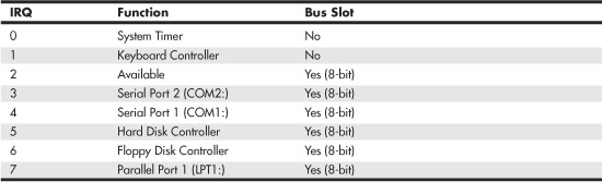
If you have a system that has one of the original 8-bit ISA buses, you will find that the IRQ resources provided by the system present a severe limitation. Installing several devices that need the services of system IRQs in a PC/XT-type system can be a study in frustration because the only way to resolve the interrupt-shortage problem is to remove the adapter board that you need the least.
16-Bit ISA, EISA, and MCA Bus Interrupts
The introduction of the AT, based on the 286 processor, was accompanied by an increase in the number of external hardware interrupts the bus would support. The number of interrupts was doubled to 16 by using two Intel 8259 interrupt controllers, piping the interrupts generated by the second one through the unused IRQ2 in the first controller. This arrangement effectively makes only 15 IRQ assignments available, and IRQ2 effectively became inaccessible.
By routing all the interrupts from the second IRQ controller through IRQ2 on the first, all these new interrupts are assigned a nested priority level between IRQ1 and IRQ3. Thus, IRQ15 ends up having a higher priority than IRQ3. Figure 4.54 shows how the two 8259 chips were wired to create the cascade through IRQ2 on the first chip.
Figure 4.54 Interrupt controller cascade wiring.
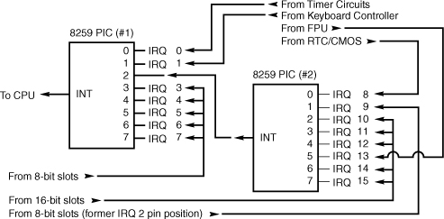
To prevent problems with boards set to use IRQ2, the AT system designers routed one of the new interrupts (IRQ9) to fill the slot position left open after removing IRQ2. This means that any card you install in a modern system that claims to use IRQ2 is really using IRQ9 instead.
Table 4.76 shows the typical uses for interrupts in the 16-bit ISA and 32-bit PCI/AGP buses and lists them in priority order from highest to lowest. The obsolete EISA and MCA buses used a similar IRQ map.
Table 4.76 16/32-Bit ISA/PCI/AGP Default Interrupt Assignments

Notice that interrupts 0, 1, 2, 8, and 13 are not on the bus connectors and are not accessible to adapter cards. Interrupts 8, 10, 11, 12, 13, 14, and 15 are from the second interrupt controller and are accessible only by boards that use the 16-bit extension connector because this is where these wires are located. IRQ9 is rewired to the 8-bit slot connector in place of IRQ2, so IRQ9 replaces IRQ2 and, therefore, is available to 8-bit cards, which treat it as though it were IRQ2.
Note
Although the 16-bit ISA bus has twice as many interrupts as systems that have the 8-bit ISA bus, you still might run out of available interrupts because only 16-bit adapters can use most of the newly available interrupts. Any 32-bit PCI adapter can be mapped to any ISA IRQs.
The extra IRQ lines in a 16-bit ISA system are of little help unless the adapter boards you plan to use enable you to configure them for one of the unused IRQs. Some devices are hard-wired so they can use only a particular IRQ, and some of the early 16-bit ISA adapters weren’t designed to use 16-bit IRQs (9–15). If you have a device that already uses that IRQ, you must resolve the conflict before installing the second adapter. If neither adapter enables you to reconfigure its IRQ use, chances are that you can’t use the two devices in the same system.
PCI Interrupts
The PCI bus supports hardware interrupts (IRQs) that can be used by PCI devices to signal to the bus that they need attention. The four PCI interrupts are called INTA#, INTB#, INTC#, and INTD#. These INTx# interrupts are level sensitive, which means that the electrical signaling enables them to be shared among PCI cards. In fact, all single-device or single-function PCI chips or cards that use only one interrupt must use INTA#. This is one of the rules in the PCI specification. If additional devices are within a chip or onboard a card, the additional devices can use INTB# through INTD#. Because there are very few multifunction PCI chips or boards, practically all the devices on a given PCI bus share INTA#.
For the PCI bus to function in a PC, the PCI interrupts must be mapped to ISA interrupts. Because ISA interrupts can’t be shared, in most cases each PCI card using INTA# on the PCI bus must be mapped to a different nonshareable ISA interrupt. For example, you could have a system with four PCI slots and four PCI cards installed, each using PCI interrupt INTA#. These cards would each be mapped to a different available ISA interrupt request, such as IRQ9, IRQ10, IRQ11, or IRQ5 in most cases.
Finding unique IRQs for each device on both the ISA and PCI buses has always been a problem; there simply aren’t enough free ones to go around. Setting two ISA devices to the same IRQ has never been possible (the so-called IRQ sharing of IRQ4 by COM1/3 and IRQ3 by COM2/4 didn’t allow both COM ports to work at the same time), but on most newer systems sharing IRQs between multiple PCI devices might be possible. Newer system BIOSs as well as plug-and-play operating systems support a function known as PCI IRQ Steering. For this to work, both your system BIOS and operating system must support IRQ Steering. Older system BIOSs and Windows 95 or 95A and earlier do not have support for PCI IRQ Steering.
Advanced Programmable Interrupt Controller
As a replacement for the traditional pair of 8259 interrupt controllers, Intel developed the Advanced Programmable Interrupt Controller (APIC) in the mid-1990s. Although all processors since the original Pentium contain an APIC, an APIC must also be present in the motherboard’s chipset, and the BIOS and operating system must also support APIC. APIC support is present on most recent motherboards and has been supported in all Windows releases since Windows 2000. In some systems you can enable or disable APIC support in the system BIOS, but in most it is permanently enabled.
APIC provides support for multiple processors, but it is also used on single-processor computers. The major benefit of APIC for a single processor is support for virtual PCI IRQs above 15. Most APIC implementations support virtual IRQs up to 24. Although Windows 2000 tends to place PCI IRQs into the traditional ISA range of 0–15, even when APIC is enabled, Windows XP and later make full use of APIC services when installed on a system with APIC enabled. With Windows XP and later, APIC limits IRQ sharing to enable devices to perform better with fewer conflicts. For example, on one typical system with APIC enabled, PCI IRQs are assigned as follows:
• PCI IRQ 16—Onboard audio/AGP graphics (shared)
• PCI IRQ 17—Add-on card USB 1.1 controller (nonshared)
• PCI IRQ 18—Add-on card USB 1.1 controller (nonshared)
• PCI IRQ 19—10/100 Ethernet adapter/add-on card USB 2.0 controller (shared)
• PCI IRQ 21—Onboard USB 1.1 controllers (3)/onboard USB 2.0 controller (shared)
The traditional ISA IRQs 0–15 on the sample system are used only for ISA devices, thus preventing ISA-PCI IRQ conflicts.
Note
APIC must be enabled in the system BIOS before x64 editions of Windows can be installed.
IRQ Conflicts
One of the more common IRQ conflicts in older systems is the potential one between the integrated COM2: port found in most modern motherboards and an internal (card-based) ISA modem. The problem stems from the fact that true PC card-based modems (not the so-called WinModems, which are software based) incorporate a serial port as part of the card’s circuitry. This serial port is set as COM2: by default. Your PC sees this as having two COM2: ports, each using the same IRQ and I/O port address resources.
The solution to this problem is easy: Enter the system BIOS Setup and disable the built-in COM2: port in the system. While you are there, you might think about disabling the COM1: port too, because you are unlikely to use it. Disabling unused COMx: ports is one of the best ways to free up a couple of IRQs for other devices to use.
![]() See “Serial Ports,” p. 791 (Chapter 14).
See “Serial Ports,” p. 791 (Chapter 14).
Note that an easy way to check your interrupt settings is to use the Device Manager in Windows. By double-clicking the Computer Properties icon in the Device Manager, you can get concise lists of all used system resources. Microsoft has also included a program in Windows 98 and later called System Information (MSinfo32), which also gives you a report of detailed system information.
To provide the maximum number of shareable interrupts in a recent system without ISA slots, I recommend performing the following steps in the system BIOS:
1. Disable any unused legacy ports in the system BIOS. For example, if you use USB ports instead of serial and parallel ports, disable the serial and parallel ports. This can free up as many as three IRQs.
2. Select the IRQs freed up in step 1 as available for PCI/PnP use. Depending on the BIOS, the screen to use might be known as the PnP/PCI Resource Exclusion screen or the PnP/PCI Configuration screen.
3. Enable the Reset Configuration Data option so the IRQ routing tables in the CMOS are cleared.
4. Save your changes and exit the BIOS setup program.
DMA Channels
Direct memory access (DMA) channels are used by communications devices that must send and receive information at high speeds. A serial or parallel port does not use a DMA channel, but an ISA-based sound card or SCSI adapter often does. DMA channels sometimes can be shared if the devices are not the type that would need them simultaneously. For example, you can have a network adapter and a tape backup adapter sharing DMA channel 1, but you can’t back up while the network is running. To back up during network operation, you must ensure that each adapter uses a unique DMA channel.
Note
There are several types of DMA in a modern PC. The DMA channels referred to in this section involve the ISA bus. Other buses, such as the ATA/IDE bus used by hard drives, have different DMA uses. The DMA channels explained here don’t involve your ATA/IDE drives, even if they are set to use DMA or Ultra DMA transfers.
8-Bit ISA Bus DMA Channels
In the 8-bit ISA bus, four DMA channels support high-speed data transfers between I/O devices and memory. Three of the channels are available to the expansion slots. Table 4.77 shows the typical uses of these DMA channels.
Table 4.77 8-Bit ISA Default DMA-Channel Assignments
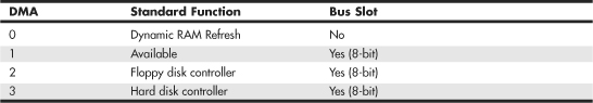
Because most systems typically have both a floppy and hard disk drive, only one DMA channel is available in 8-bit ISA systems.
16-Bit ISA DMA Channels
Since the introduction of the 286 CPU, the ISA bus has supported eight DMA channels, with seven channels available to the expansion slots. Similar to the expanded IRQ lines described earlier in this chapter, the added DMA channels were created by cascading a second DMA controller to the first one. DMA channel 4 is used to cascade channels 0–3 to the microprocessor. Channels 0–3 are available for 8-bit transfers, and channels 5–7 are for 16-bit transfers only. Table 4.78 shows the typical uses for the DMA channels.
Table 4.78 16-Bit ISA Default DMA-Channel Assignments

Note that PCI adapters don’t use these ISA DMA channels; these are only for ISA cards. However, some PCI cards emulate the use of these DMA channels (such as sound cards) to work with older software.
The only standard DMA channel used in all systems is DMA 2, which is universally used by the floppy controller. DMA 4 is not usable and does not appear in the bus slots. DMA channels 1 and 5 are most commonly used by ISA sound cards, such as the Sound Blaster 16, or by newer PCI sound cards that emulate an older one for backward compatibility. These cards use both an 8-bit and a 16-bit DMA channel for high-speed transfers. DMA 3 is used when a parallel port is configured to work in ECP mode or EPP/ECP mode. Some nonstandard systems, such as older Packard Bell computers, use DMA 1 instead of DMA 3 for the parallel port by default. However, a jumper block on the motherboard on many of these systems can be set to use DMA 3 for the parallel port and avoid conflicts with sound cards that use DMA 1.
Note
Although DMA channel 0 appears in a 16-bit slot connector extension and therefore can be used only by a 16-bit card, it performs only 8-bit transfers! Because of this, you generally don’t see DMA 0 as a choice on 16-bit cards. Most 16-bit cards (such as SCSI host adapters) that use DMA channels have their choices limited to DMA 5–7.
I/O Port Addresses
Your computer’s I/O ports enable communications between devices and software in your system. They are equivalent to two-way radio channels. If you want to talk to your serial port, you need to know on which I/O port (radio channel) it is listening. Similarly, if you want to receive data from the serial port, you need to listen on the same channel on which it is transmitting.
Unlike IRQs and DMA channels, our systems have an abundance of I/O ports. There are exactly 65,536 ports—numbered from 0000h to FFFFh—which is a feature of the Intel x86 processor design. Even though most devices use up to eight ports for themselves, with that many to spare, you won’t run out anytime soon. The biggest problem you have to worry about is setting two devices to use the same port.
Most modern plug-and-play systems resolve any port conflicts and select alternative ports for one of the conflicting devices.
One confusing issue is that I/O ports are designated by hexadecimal addresses similar to memory addresses. They are not memory; they are ports. The difference is that when you send data to memory address 1000h, it gets stored in your SIMM or DIMM memory. If you send data to I/O port address 1000h, it gets sent out on the bus on that “channel,” and anybody listening in could then “hear” it. If nobody is listening to that port address, the data reaches the end of the bus and is absorbed by the bus terminating resistors.
Driver programs are primarily what interact with devices at the various port addresses. The driver must know which ports the device is using to work with it, and vice versa. That is not usually a problem because the driver and device come from the same company.
Motherboard and chipset devices usually are set to use I/O port addresses 0h–FFh, and all other devices use 100h–FFFFh. Table 4.79 shows the commonly used motherboard and chipset-based I/O port usage.
Table 4.79 Motherboard and Chipset-Based Device Port Addresses

To find out exactly which port addresses are being used on your motherboard, consult the board documentation or look up these settings in the Windows Device Manager.
Bus-based devices typically use the addresses from 100h on up. Table 4.80 lists the commonly used bus-based device addresses and some common adapter cards and their settings.
Table 4.80 Bus-Based Device Port Addresses


To find out exactly what your devices are using, again I recommend consulting the documentation for the device or looking up the device in the Windows Device Manager. Note that the documentation for some devices might list only the starting address instead of the full range of I/O port addresses used.
Virtually all devices on the system buses use I/O port addresses. Most of these are fairly standardized, meaning conflicts or problems won’t often occur with these settings. In the next section, you learn more about working with I/O addresses.
Resolving Resource Conflicts
The resources in a system are limited. Unfortunately, the demands on those resources seem to be unlimited. As you add more and more adapter cards to your system, you will find that the potential for resource conflicts increases. If your system is fully PnP-compatible, potential conflicts should be resolved automatically, but often are not.
How do you know whether you have a resource conflict? Typically, one of the devices in your system stops working. Resource conflicts can exhibit themselves in other ways, though. Any of the following events could be diagnosed as a resource conflict:
• A device transfers data inaccurately.
• Your system frequently locks up.
• Your sound card doesn’t sound quite right.
• Your mouse doesn’t work.
• Garbage appears on your video screen for no apparent reason.
• Your printer prints gibberish.
• You can’t format a floppy disk.
• The PC starts in Safe mode (Windows 9x/Me) or can start only in Last Known Good Configuration (Windows 2000 and newer).
Windows also shows conflicts by highlighting a device in yellow or red in the Device Manager representation. By using the Windows Device Manager, you can usually spot the conflicts quickly.
In the following sections, you learn some of the steps you can take to head off resource conflicts or track them down when they occur.
Tip
The serial, PS/2 mouse, and parallel ports still found in many recent systems are all ISA devices that cannot share IRQs. If you no longer use these ports, you can use these devices’ IRQs for other devices if you do the following:
• Disable the unused port in the system BIOS.
• Configure the system BIOS to use the IRQ formerly used by the device(s) for PnP configuration (this might be automatic in some systems).
Another way you can help is to install cards in a particular sequence, and not all at once. Modifying the installation sequence often helps because many cards can use only one or two out of a predefined selection of IRQs that is specific to each brand or model of card. When the cards are installed in a controlled sequence, the plug-and-play software can more easily work around IRQ conflicts caused by the default configurations of different cards.
On initial startup I recommend a minimum configuration with only the graphics card, memory, and storage drives. This allows for the least possibility of system conflicts in the initial configuration. If your motherboard came with drivers specific to the chipset or other built-in features of the board, now is the time to load or install them. Complete the configuration of all built-in devices before installing any other cards or external devices.
After the basic system has been configured (and after you have successfully loaded your operating system and any updates or patches), you can then begin adding one device at a time in a specific order. So, you will power down, install the new device, power up, and proceed to install any necessary drivers and configure the device. You’ll probably have to restart your system after you are done to fully complete the configuration.
Tip
I sometimes recommend that between installing devices you enter the Device Manager in Windows and print out the resource settings as they are configured at the time. This way, you have a record of how the configuration changes during the entire device installation and configuration process.
Here’s the loading sequence for additional cards:
1. Sound card
2. Internal or external modem
3. Network card
4. Auxiliary video devices, such as MPEG decoders, 3D accelerators, and so on
5. SCSI adapter
6. Anything else
Normally, using this controlled sequence of configuring or building up your system results in easier integration with fewer conflicts and configuration hassles.
Using a System-Configuration Template
A system-configuration template is helpful because remembering something that is written down is easier than keeping it in your head.
I like to use a worksheet split into three main areas—one for interrupts, another for DMA channels, and a middle area for devices that do not use interrupts. Each section lists the IRQ or DMA channel on the left and the I/O port device range on the right. This way, I get the clearest picture of which resources are used and which ones are available in a given system.
This type of configuration sheet is resource based instead of component based. Each row in the template represents a different resource and lists the component using the resource as well as the resources used. The chart has pre-entered all the fixed items in a modern PC for which the configuration cannot be changed.
To fill out this type of chart, you would perform the following steps:
1. Enter the default resources used by standard components, such as serial and parallel ports, disk controllers, and video. You can use the filled-out example I have provided to see how most standard devices are configured.
2. Enter the default resources used by additional add-on components, such as sound cards, network cards, and so on. In the case of PnP hardware, there are no real defaults. Instead, use Windows Device Manager or comparable diagnostic programs to determine the settings used for the device.
3. Change any configuration items that are in conflict. Try to leave built-in devices, as well as sound cards, at their default settings. Other installed adapters may have their settings changed, but be sure to document the changes.
Of course, a template such as this is best used when you’re first installing components, not after. After you have it completely filled out to match your system, you can label it and keep it with the system. Whenever you add more devices, the template will be your guide as to how any new devices should be configured if you need to configure devices manually.
Note
Thanks to plug-and-play configuration, the days of fixed IRQ and other hardware resources are over. Don’t be surprised if your system has assigned different IRQ, I/O port address, or DMA settings after you install a new card. That’s why I recommend recording information both before and after you add a new device to your system.
You also might want to track which PCI slot is used by a particular card because some systems convert PCI IRQs to different ISA IRQs depending on which slot is used for a card. Also, some systems pair PCI slots or might pair the AGP slot and a PCI slot, assigning cards installed in both paired slots to the same ISA IRQ. Check the system or motherboard documentation to determine which slots and onboard devices share a particular IRQ.


Plug-and-Play Systems
Plug and Play (PnP) represents a major revolution in interface technology. PnP first came on the market in 1995, and most motherboards and adapter cards since 1996 take advantage of it. Prior to that, PC users were forced to muddle through a nightmare of DIP switches and jumpers every time they wanted to add new devices to their systems. The results, all too often, were system resource conflicts and nonfunctioning cards.
PnP was not an entirely new concept. It was a key design feature of MCA and EISA interfaces that preceded it by almost 10 years, but the limited appeal of MCA and EISA meant that they never became true de facto industry standards. Therefore, mainstream PC users still had to worry about I/O addresses, DMA channels, and IRQ settings. Early PCI-based systems also used a form of PnP configuration, but because there was no provision for managing conflicts between PCI and ISA cards, many users still had configuration problems. But now that PnP has become prevalent, worry-free hardware setup is available to all computer buyers.
For PnP to work, the following components are desired:
• PnP BIOS
Each of these components needs to be PnP compatible, meaning that it complies with the PnP specifications. Of course, support for these features is found in all modern systems.
The Hardware Component
The hardware component refers to both computer systems and adapter cards. The term does not mean, however, that you can’t use your older ISA adapter cards (referred to as legacy cards) in a PnP system. You can use these cards; in fact, your PnP BIOS automatically reassigns PnP-compatible cards around existing legacy components. Also, many late-model ISA cards can be switched into PnP-compatible mode.
PnP adapter cards communicate with the system BIOS and the operating system to convey information about which system resources are necessary. The BIOS and operating system, in turn, resolve conflicts (wherever possible) and inform the adapter card which specific resources it should use. The adapter card then can modify its configuration to use the specified resources.
The BIOS Component
The BIOS component means that most users of pre-1996 PCs need to update their BIOSs or purchase new machines that have PnP BIOSs. For a BIOS to be compatible, it must support 13 additional system function calls, which can be used by the OS component of a PnP system. The PnP BIOS specification was developed jointly by Compaq, Intel, and Phoenix Technologies.
The PnP features of the BIOS are implemented through an expanded POST. The BIOS is responsible for identification, isolation, and possible configuration of PnP adapter cards. The BIOS accomplishes these tasks by performing the following steps:
1. Disables any configurable devices on the motherboard or on adapter cards.
2. Identifies any PnP PCI or ISA devices.
3. Compiles an initial resource-allocation map for ports, IRQs, DMAs, and memory.
4. Enables I/O devices.
5. Scans the ROMs of ISA devices.
6. Configures initial program-load (IPL) devices, which are used later to boot the system.
7. Enables configurable devices by informing them which resources have been assigned to them.
8. Starts the bootstrap loader.
9. Transfers control to the operating system.
The Operating System Component
The operating system component is found in most modern operating systems since Windows 95. In some cases system manufacturers have provided extensions to the operating system for their specific hardware. Such is especially true for notebook systems, for example. Be sure you load these extensions if they are required by your system.
It is the responsibility of the operating system to inform users of conflicts that can’t be resolved by the BIOS. Depending on the sophistication of the operating system, the user then could configure the offending cards manually (onscreen) or turn off the system and set switches on the physical cards. When the system is restarted, it is checked for remaining (or new) conflicts, any of which are brought to the user’s attention. Through this repetitive process, all system conflicts are resolved.
Note
Because of revisions in some of the Plug and Play specifications, especially the ACPI specification, it can help to ensure you are running the latest BIOS and drivers for your system. With the flash ROM used in most PnP systems, you can download the new BIOS image from the system vendor or manufacturer and run the supplied BIOS update program.
Motherboard Selection Criteria (Knowing What to Look For)
I am often asked to make recommendations for purchases. Without guidance, many individuals don’t have any rhyme or reason to their selections and instead base their choices solely on magazine reviews or, even worse, on some personal bias. To help eliminate this haphazard selection process, I have developed a simple motherboard selection checklist.
It helps to think like an engineer when you make your selection. Consider every aspect and detail of the motherboards in question. For instance, you should consider both present usage as well as any future uses and upgrades. Technical support at a professional (as opposed to a user) level is extremely important. Check for manual and driver downloads: Are they easy to find and up to date? The following list includes some of the most important criteria to consider when selecting a motherboard:
• Motherboard chipset—The motherboard chipset is the backbone of a system and is perhaps the single most important part you’ll consider. Compare the features of the available chipsets to ensure that the board will do what you want. For example, some chipsets include support for faster memory, PCIe 2.x cards, SATA 3Gbps drives, and optional RAID capabilities. I spend the most time deciding on my next chipset because it affects and influences virtually every other component in the system.
• Processor socket—The processor socket on a motherboard dictates the specific processor makes and models you will be able to install. In most cases you will have a given processor in mind, so choose a motherboard with a socket that supports the processor you wish to use. The main sockets in use today on new systems include Socket AM2 and AM3 for AMD processors, and Sockets LGA775, LGA1156, and LGA1366 for Intel processors. See Table 4.6 (which lists CPU socket specifications) to see what types of processors are supported by each socket. Also check the motherboard specifications for what specific processors are supported by a given motherboard.
• Memory—The type and amount of memory compatible with a system depends on the motherboard you choose. Most motherboards today support either DDR2 or DDR3 memory, in either single-, dual-, or triple-channel operation. The number of memory sockets, supported speeds, and other variables also depend on the motherboard, so check the board specifications to see exactly what is supported.
• Form factor—The form factor indicates the size and shape of the board, and must be compatible with the chassis or case and power supply. For maximum flexibility, performance, reliability, and ease of use, I recommend motherboards based on the ATX and microATX form factors. Larger form factors such as ATX offer more slots and room for additional integrated components and features. Smaller variations on ATX are also available, but in the end you need to be sure that the motherboard is compatible with the case and power supply you have chosen.
• Bus slots—Current systems offer one to five or more PCI and PCI Express slots (depending on the form factor). Some boards have more than one PCIe x16 (video card) slots, which you may want if you are running multiple video cards in an SLI or CrossFire arrangement. Make sure the board you choose has the number and types of slots you require.
• Onboard ATA interfaces—All motherboards on the market have included onboard Serial and Parallel ATA interfaces for some time now, but not all are equal. Look for boards that include at least four to six SATA connectors, with support for 3Gbps operation as well as optional RAID functionality (if desired).
• Other built-in interfaces—Ideally, a motherboard should contain as many built-in standard controllers and interfaces as possible. Most boards feature integrated USB, sound, and LAN (look for those offering gigabit Ethernet), whereas others also have integrated video, FireWire, eSATA, dual LAN adapters, and more.
Tip
With a never-ending stream of motherboards coming onto the market, finding motherboards with the features you want can be difficult. Online shopping sites such as NewEgg (www.newegg.com) can be useful for finding out what types of boards are currently available, but for a more comprehensive search, Motherboard Homeworld’s Mobot search engine helps you find both current and older motherboards based on your choice of form factor, platform, chipset, CPU type, processor, manufacturer, memory type, slot types, built-on ports, and more. Check it out at www.motherboards.org/mobot.
• Documentation—Good technical documentation is important. Documents should be easy to download from the manufacturer’s site, and should include information on any and all jumpers and switches found on the board, connector pinouts for all connectors, specifications for other plug-in components, and any other applicable technical information. Most vendors provide this information in electronic form (using the Adobe Reader PDF format) on their websites, so you can preview the information available for a given motherboard before you buy.
• Technical support—Good online technical support goes beyond documentation. It includes easily downloadable driver and BIOS updates, FAQs, updated tables of processor and memory compatibility, and utility programs to help you monitor the condition of your system. In addition to these online support features, make sure the vendor can be contacted through email and by phone.
Most of the time I recommend purchasing boards from better-known motherboard manufacturers such as GIGABYTE, Foxconn, Intel, and others. These boards might cost a little more, but there is some safety in the more well-known brands. That is, the more boards they sell, the more likely that any problems will have been discovered by others and solved long before you get yours. Also, if service or support is necessary, the larger vendors are more likely to be around in the long run.
Chipset Documentation
As mentioned, documentation is an important factor to consider when you’re planning to purchase a motherboard. Most motherboard manufacturers design their boards around a particular chipset, which actually counts as the bulk of the motherboard circuitry. I recommend downloading the chipset datasheets or other technical documentation directly from the chipset manufacturer.
For example, one of the more common questions I hear about a system relates to the BIOS Setup program. People want to know what the “Advanced Chipset Setup” features mean and what the effects of changing them will be. Often they go to the BIOS manufacturer thinking that the BIOS documentation will offer help. Usually, however, people find that there is no real coverage of what the chipset setup features are in the BIOS documentation. You will find this information in the data book provided by the chipset manufacturer. Although these books are meant to be read by the engineers who design the boards, they contain all the detailed information about the chipset’s features, especially those that might be adjustable. With the chipset data book, you will have an explanation of all the controls in the Advanced Chipset Setup section of the BIOS Setup program.
Besides the main chipset datasheets, I also recommend collecting any data books on the other major chips in the system. This includes Super I/O chips, SATA controllers, and of course the main processor. You will find an incredible amount of information on these components in the datasheets.