
Chapter 3. Processor Types and Specifications
Microprocessor History
The brain or engine of the PC is the processor—sometimes called microprocessor or central processing unit (CPU). The CPU performs the system’s calculating and processing. The processor is often the most expensive single component in the system (although graphics card pricing often surpasses it); in higher-end systems it can cost up to four or more times more than the motherboard it plugs into. Intel is generally credited with creating the first microprocessor in 1971 with the introduction of a chip called the 4004. Today Intel still has control over the processor market, at least for PC systems, although AMD has garnered a respectable market share. For the most part, PC-compatible systems use either Intel processors or Intel-compatible processors from a handful of competitors such as AMD and VIA/Cyrix.
It is interesting to note that the microprocessor had existed for only 10 years prior to the creation of the PC! Intel released the first microprocessor in 1971; the PC was created by IBM in 1981. Nearly three decades later, we are still using systems based more or less on the design of that first PC. The processors powering our PCs today are still backward compatible in many ways with the Intel 8088 that IBM selected for the first PC in 1981.
The First Microprocessor
Intel was founded on July 18, 1968 (as N M Electronics) by two ex-Fairchild engineers, Robert Noyce and Gordon Moore. Almost immediately they changed the company name to Intel and were joined by cofounder Andrew Grove. They had a specific goal: to make semiconductor memory practical and affordable. This was not a given at the time, considering that silicon chip-based memory was at least 100 times more expensive than the magnetic core memory commonly used in those days. At the time, semiconductor memory was going for about a dollar a bit, whereas core memory was about a penny a bit. Noyce said, “All we had to do was reduce the cost by a factor of a hundred, then we’d have the market; and that’s basically what we did.”
By 1970, Intel was known as a successful memory chip company, having introduced a 1Kb memory chip, much larger than anything else available at the time. (1Kb equals 1,024 bits, and a byte equals 8 bits. This chip, therefore, stored only 128 bytes—not much by today’s standards.) Known as the 1103 dynamic random access memory (DRAM), it became the world’s largest-selling semiconductor device by the end of the following year. By this time, Intel had also grown from the core founders and a handful of others to more than 100 employees.
Because of Intel’s success in memory chip manufacturing and design, Japanese manufacturer Busicom asked Intel to design a set of chips for a family of high-performance programmable calculators. At the time, all logic chips were custom-designed for each application or product. Because most chips had to be custom-designed specific to a particular application, no one chip could have any widespread usage.
Busicom’s original design for its calculator called for at least 12 custom chips. Intel engineer Ted Hoff rejected the unwieldy proposal and instead proposed a single-chip, general-purpose logic device that retrieved its application instructions from semiconductor memory. As the core of a four-chip set including ROM, RAM, I/O and the 4004 processor, a program could control the processor and essentially tailor its function to the task at hand. The chip was generic in nature, meaning it could function in designs other than calculators. Previous chip designs were hard-wired for one purpose, with built-in instructions; this chip would read a variable set of instructions from memory, which would control the function of the chip. The idea was to design, on a single chip, almost an entire computing device that could perform various functions, depending on which instructions it was given.
In April 1970 Intel hired Frederico Faggin to design and create the 4004 logic based on the proposal by Hoff. Like the Intel founders, Faggin also came from Fairchild Semiconductor, where he had developed the silicon gate technology that would prove essential to good microprocessor design. During the initial logic design and layout process, Faggin had help from Masatoshi Shima, the engineer at Busicom responsible for the calculator design. Shima worked with Faggin until October 1970, after which he returned to Busicom. Faggin recieved the first finished batch of 4004 chips at closing time one day in January 1971, and worked alone until early the next morning testing the chip before declaring “It works!” The 4000 chip family was completed by March 1971, and put into production by June 1971. It is interesting to note that Faggin actually signed the processor die with his initials (F.F.), a tradition that was often carried on by others in subsequent chip designs.
There was one problem with the new chip: Busicom owned the rights to it. Faggin knew that the product had almost limitless application, bringing intelligence to a host of “dumb” machines. He urged Intel to repurchase the rights to the product. While Intel founders Gordon Moore and Robert Noyce championed the new chip, others within the company were concerned that the product would distract Intel from its main focus—making memory. They were finally convinced by the fact that every four-chip microcomputer set included two memory chips. As the director of marketing at the time recalled, “Originally, I think we saw it as a way to sell more memories, and we were willing to make the investment on that basis.”
Intel offered to return Busicom’s $60,000 investment in exchange for the rights to the product. Struggling with financial troubles, the Japanese company agreed. Nobody in the industry at the time, even Intel, realized the significance of this deal, which paved the way for Intel’s future in processors.
The result was the November 15, 1971 introduction of the 4-bit Intel 4004 CPU as part of the MCS-4 microcomputer set. The 4004 ran at a maximum clock speed of 740KHz (740,000 cycles per second, or nearly 3/4ths of a megahertz), contained 2,300 transistors in an area of only 12 sq. mm (3.5mm x 3.5mm), and was built on a 10-micron process, where each transistor was spaced about 10 microns (millionths of a meter) apart. Data was transferred 4 bits at a time, and the maximum addressable memory was only 640 bytes. The chip cost about $200 and delivered about as much computing power ENIAC, one of the first electronic computers. By comparison, ENIAC relied on 18,000 vacuum tubes packed into 3,000 cubic feet (85 cubic meters) when it was built in 1946.
The 4004 was designed for use in a calculator but proved to be useful for many other functions because of its inherent programmability. For example, the 4004 was used in traffic light controllers, blood analyzers, and even in the NASA Pioneer 10 deep-space probe. You can see more information about the legendary 4004 processor at www.intel4004.com and www.4004.com.
In April 1972, Intel released the 8008 processor, which originally ran at a clock speed of 500KHz (0.5MHz). The 8008 processor contained 3,500 transistors and was built on the same 10-micron process as the previous processor. The big change in the 8008 was that it had an 8-bit data bus, which meant it could move data 8 bits at a time—twice as much as the previous chip. It could also address more memory, up to 16KB. This chip was primarily used in dumb terminals and general-purpose calculators.
The next chip in the lineup was the 8080, introduced in April 1974. The 8080 was concieved by Frederico Faggin and designed by Masatoshi Shima (former Busicom engineer) under Faggin’s supervision. Running at a clock rate of 2MHz, the 8080 processor had 10 times the performance of the 8008. The 8080 chip contained 6,000 transistors and was built on a 6-micron process. Similar to the previous chip, the 8080 had an 8-bit data bus, so it could transfer 8 bits of data at a time. The 8080 could address up to 64KB of memory, significantly more than the previous chip.
It was the 8080 that helped start the PC revolution because this was the processor chip used in what is generally regarded as the first personal computer, the Altair 8800. The CP/M operating system was written for the 8080 chip, and the newly founded Microsoft delivered its first product: Microsoft BASIC for the Altair. These initial tools provided the foundation for a revolution in software because thousands of programs were written to run on this platform.
In fact, the 8080 became so popular that it was cloned. Wanting to focus on processors, Frederico Faggin left Intel in 1974 to found Zilog and create a “Super-80” chip, a high performance 8080 compatible processor. Masatoshi Shima joined Zilog in April 1975 to help design what became known as the Z80 CPU. The Z80 was released in July 1976 and became one of the most successful processors in history, in fact it is still being manufactured and sold today. The Z80 was not pin compatible with the 8080, but instead combined functions such as the memory interface and RAM refresh circuitry, which enabled cheaper and simpler systems to be designed. The Z80 incorporated a superset of 8080 instructions, meaning it could run all 8080 programs. It also included new instructions and new internal registers, so while 8080 software would run on the Z80, software designed for the Z80 would not necessarily run on the older 8080. The Z80 ran initially at 2MHz (later versions ran up to 20MHz), contained 8,500 transistors, and could access 64KB of memory.
RadioShack selected the Z80 for the TRS-80 Model 1, its first PC. The chip also was the first to be used by many pioneering personal computer systems, including the Osborne and Kaypro machines. Other companies followed, and soon the Z80 was the standard processor for systems running the CP/M operating system and the popular software of the day.
Intel released the 8085, its follow-up to the 8080, in March 1976. The 8085 ran at 5MHz and contained 6,500 transistors. It was built on a 3-micron process and incorporated an 8-bit data bus. Even though it predated the Z80 by several months, it never achieved the popularity of the Z80 in personal computer systems. It was however used in the IBM System/23 Datamaster, which was the immediate predecessor to the original PC at IBM. The 8085 became most popular as an embedded controller, finding use in scales and other computerized equipment.
Along different architectural lines, MOS Technologies introduced the 6502 in 1976. This chip was designed by several ex-Motorola engineers who had worked on Motorola’s first processor, the 6800. The 6502 was an 8-bit processor like the 8080, but it sold for around $25, whereas the 8080 cost about $300 when it was introduced. The price appealed to Steve Wozniak, who placed the chip in his Apple I and Apple ][/][+ designs. The chip was also used in systems by Commodore and other system manufacturers. The 6502 and its successors were also used in game consoles, including the original Nintendo Entertainment System (NES) among others. Motorola went on to create the 68000 series, which became the basis for the original line of Apple Macintosh computers. The second-generation Macs used the PowerPC chip, also by Motorola and a successor to the 68000 series. Of course, the current Macs have adopted PC architecture, using the same processors, chipsets, and other components as PCs.
In the early 1980s, I had a system containing both a MOS Technologies 6502 and a Zilog Z80. It was a 1MHz (yes, that’s one megahertz!) 6502-based Apple ][+ system with a Microsoft Softcard (Z80 card) plugged into one of the slots. The Softcard contained a 2MHz Z80 processor, which enabled me to run both Apple and CP/M software on the system.
All these previous chips set the stage for the first PC processors. Intel introduced the 8086 in June 1978. The 8086 chip brought with it the original x86 instruction set that is still present in current x86-compatible chips such as the Core i Series and AMD Phenom II. A dramatic improvement over the previous chips, the 8086 was a full 16-bit design with 16-bit internal registers and a 16-bit data bus. This meant that it could work on 16-bit numbers and data internally and also transfer 16 bits at a time in and out of the chip. The 8086 contained 29,000 transistors and initially ran at up to 5MHz. The chip also used 20-bit addressing, so it could directly address up to 1MB of memory. Although not directly backward compatible with the 8080, the 8086 instructions and language were very similar and enabled older programs to quickly be ported over to run. This later proved important to help jumpstart the PC software revolution with recycled CP/M (8080) software.
The fate of both Intel and Microsoft was dramatically changed in 1981 when IBM introduced the IBM PC, which was based on a 4.77MHz Intel 8088 processor running the Microsoft Disk Operating System (MS-DOS) 1.0. Since that fateful decision was made to use an Intel processor in the first PC, subsequent PC-compatible systems have used a series of Intel or Intel-compatible processors, with each new one capable of running the software of the processor before it.
Although the 8086 was a great chip, it required expensive 16-bit board designs and infrastructure to support it. To help bring costs down, in 1979 Intel released what some called a crippled version of the 8086 called the 8088. The 8088 processor used the same internal core as the 8086, had the same 16-bit registers, and could address the same 1MB of memory, but the external data bus was reduced to 8 bits. This enabled support chips from the older 8-bit 8085 to be used, and far less expensive boards and systems could be made. These reasons are why IBM chose the 8088 instead of the 8086 for the first PC.
This decision would affect history in several ways. The 8088 was fully software compatible with the 8086, so it could run 16-bit software. Also, because the instruction set was very similar to the previous 8085 and 8080, programs written for those older chips could be quickly and easily modified to run. This enabled a large library of programs to be quickly released for the IBM PC, thus helping it become a success. The overwhelming blockbuster success of the IBM PC left in its wake the legacy of requiring backward compatibility with it. To maintain the momentum, Intel has pretty much been forced to maintain backward compatibility with the 8088/8086 in most of the processors it has released since then.
PC Processor Evolution
Since the first PC came out in 1981, PC processor evolution has concentrated on four main areas:
• Increasing transistor count and density
• Increasing clock cycling speeds
• Increasing the size of internal registers (bits)
• Increasing the number of cores in a single chip
Intel introduced the 286 chip in 1982. With 134,000 transistors, it provided about three times the performance of other 16-bit processors of the time. Featuring on-chip memory management, the 286 also offered software compatibility with its predecessors. This revolutionary chip was first used in IBM’s benchmark PC-AT, the system upon which all modern PCs are based.
In 1985 came the Intel 386 processor. With a new 32-bit architecture and 275,000 transistors, the chip could perform more than five million instructions every second (MIPS). Compaq’s Deskpro 386 was the first PC based on the new microprocessor.
Next out of the gate was the Intel 486 processor in 1989. The 486 had 1.2 million transistors and the first built-in math coprocessor. It was some 50 times faster than the original 4004, equaling the performance of some mainframe computers.
Then, in 1993, Intel introduced the first P5 family (586) processor, called the Pentium, setting new performance standards with several times the performance of the previous 486 processor. The Pentium processor used 3.1 million transistors to perform up to 90 MIPS—now up to about 1,500 times the speed of the original 4004.
Note
Intel’s change from using numbers (386/486) to names (Pentium/Pentium Pro) for its processors was based on the fact that it could not secure a registered trademark on a number and therefore could not prevent its competitors from using those same numbers on clone chip designs.
The first processor in the P6 (686) family, called the Pentium Pro processor, was introduced in 1995. With 5.5 million transistors, it was the first to be packaged with a second die containing high-speed L2 memory cache to accelerate performance.
Intel revised the original P6 (686/Pentium Pro) and introduced the Pentium II processor in May 1997. Pentium II processors had 7.5 million transistors packed into a cartridge rather than a conventional chip, allowing the L2 cache chips to be attached directly on the module. The Pentium II family was augmented in April 1998, with both the low-cost Celeron processor for basic PCs and the high-end Pentium II Xeon processor for servers and workstations. Intel followed with the Pentium III in 1999, essentially a Pentium II with Streaming SIMD Extensions (SSE) added.
Around the time the Pentium was establishing its dominance, AMD acquired NexGen, who had been working on its Nx686 processor. AMD incorporated that design along with a Pentium interface into what would be called the AMD K6. The K6 was both hardware and software compatible with the Pentium, meaning it plugged in to the same Socket 7 and could run the same programs. As Intel dropped its Pentium in favor of the more expensive Pentium II and III, AMD continued making faster versions of the K6 and made huge inroads in the low-end PC market.
During 1998, Intel became the first to integrate L2 cache directly on the processor die (running at the full speed of the processor core), dramatically increasing performance. This was first done on the second-generation Celeron processor (based on the Pentium II core), as well as the Pentium IIPE (performance-enhanced) chip used only in laptop systems. The first high-end desktop PC chip with on-die full-core speed L2 cache was the second-generation (Coppermine core) Pentium III introduced in late 1999. After this, all major processor manufacturers began integrating L2 (and even L3) cache on the processor die, a trend that continues today.
AMD introduced the Athlon in 1999 to compete with Intel head to head in the high-end desktop PC market. The Athlon became very successful, and it seemed for the first time that Intel had some real competition in the higher-end systems. In hindsight the success of the Athlon might be easy to see, but at the time it was introduced, its success was anything but assured. Unlike the previous K6 chips, which were both hardware and software compatible with Intel processors, the Athlon was only software compatible and required a motherboard with an Athlon supporting chipset and processor socket.
The year 2000 saw a significant milestone when both Intel and AMD crossed the 1GHz barrier, a speed that many thought could never be accomplished. In 2001, Intel introduced a Pentium 4 version running at 2GHz, the first PC processor to achieve that speed. November 15, 2001 marked the 30th anniversary of the microprocessor, and in those 30 years processor speed had increased more than 18,500 times (from 0.108MHz to 2GHz). AMD also introduced the Athlon XP, based on its newer Palomino core, as well as the Athlon MP, designed for multiprocessor server systems.
In 2002, Intel released a Pentium 4 version running at 3.06GHz, the first PC processor to break the 3GHz barrier, and the first to feature Intel’s Hyper-Threading (HT) technology, which turns the processor into a virtual dual-processor configuration. By running two application threads at the same time, HT-enabled processors can perform tasks at speeds 25%–40% faster than non-HT-enabled processors can. This encouraged programmers to write multithreaded applications, which would prepare them for when true multicore processors would be released a few years later.
In 2003, AMD released the first 64-bit PC processor: the Athlon 64 (previously code named ClawHammer, or K8), which incorporated AMD-defined x86-64 64-bit extensions to the IA-32 architecture typified by the Athlon, Pentium 4, and earlier processors. That year Intel also released the Pentium 4 Extreme Edition, the first consumer-level processor that incorporated L3 cache. The whopping 2MB of cache added greatly to the transistor count as well as performance. In 2004, Intel followed AMD by adding the AMD-defined x86-64 extensions to the Pentium 4.
In 2005, both Intel and AMD released their first dual-core processors, basically integrating two processors into a single chip. Although boards supporting two or more processors had been commonly used in network servers for many years prior, this brought dual-CPU capabilities in an affordable package to standard PCs. Rather than attempting to increase clock rates, as has been done in the past, adding processing power by integrating two or more processors into a single chip enables future processors to perform more work with fewer bottlenecks and with a reduction in both power consumption and heat production.
In 2006, Intel released a new processor family called the Core 2, based on an architecture that came mostly from previous mobile Pentium M/Core duo processors. The Core 2 was released in a dual-core version first, followed by a quad-core version (combining two dual-core die in a single package) later in the year. In 2007, AMD released the Phenom, which was the first quad-core PC processor with all four cores on a single die. In 2008, Intel released the Core i Series (Nehalem) processors, which are single-die quad-core chips with Hyper-Threading (appearing as eight cores to the OS) that include integrated memory and optional video controllers.
16-bit to 64-bit Architecture Evolution
The first major change in processor architecture was the move from the 16-bit internal architecture of the 286 and earlier processors to the 32-bit internal architecture of the 386 and later chips, which Intel calls IA-32 (Intel Architecture, 32-bit). Intel’s 32-bit architecture dates to 1985, and it took a full 10 years for both a partial 32-bit mainstream OS (Windows 95) as well as a full 32-bit OS requiring 32-bit drivers (Windows NT) to surface, and another 6 years for the mainstream to shift to a fully 32-bit environment for the OS and drivers (Windows XP). That’s a total of 16 years from the release of 32-bit computing hardware to the full adoption of 32-bit computing in the mainstream with supporting software. I’m sure you can appreciate that 16 years is a lifetime in technology.
Now we are in the midst of another major architectural jump, as Intel, AMD, and Microsoft are in the process of moving from 32-bit to 64-bit architectures. In 2001, Intel had introduced the IA-64 (Intel Architecture, 64-bit) in the form of the Itanium and Itanium 2 processors, but this standard was something completely new and not an extension of the existing 32-bit technology. IA-64 was first announced in 1994 as a CPU development project with Intel and HP (code-named Merced), and the first technical details were made available in October 1997.
The fact that the IA-64 architecture is not an extension of IA-32 but is instead a whole new and completely different architecture is fine for non-PC environments such as servers (for which IA-64 was designed), but the PC market has always hinged on backward compatibility. Even though emulating IA-32 within IA-64 is possible, such emulation and support is slow.
With the door now open, AMD seized this opportunity to develop 64-bit extensions to IA-32, which it calls AMD64 (originally known as x86-64). Intel eventually released its own set of 64-bit extensions, which it calls EM64T or IA-32e mode. As it turns out, the Intel extensions are almost identical to the AMD extensions, meaning they are software compatible. It seems for the first time that Intel has unarguably followed AMD’s lead in the development of PC architecture.
To make 64-bit computing a reality, 64-bit operating systems and 64-bit drivers are also needed. Microsoft began providing trial versions of Windows XP Professional x64 Edition (which supports AMD64 and EM64T) in April 2005, but it wasn’t until the release of Windows Vista x64 in 2007 that 64-bit computing would begin to go mainstream. Initially, the lack of 64-bit drivers was a problem, but by the release of Windows 7 x64 in 2009, most device manufacturers provide both 32-bit and 64-bit drivers for virtually all new devices. Linux is also available in 64-bit versions, making the move to 64-bit computing possible for non-Windows environments as well.
Another important development is the introduction of multicore processors from both Intel and AMD. Current multicore processors have up to four or more full CPU cores operating off of one CPU package—in essence enabling a single processor to perform the work of multiple processors. Although multicore processors don’t make games that use single execution threads play faster, multicore processors, like multiple single-core processors, split up the workload caused by running multiple applications at the same time. If you’ve ever tried to scan for malware while simultaneously checking email or running another application, you’ve probably seen how running multiple applications can bring even the fastest processor to its knees. With multicore processors available from both Intel and AMD, your ability to get more work done in less time by multitasking is greatly enhanced. Current multicore processors also support 64-bit extensions, enabling you to enjoy both multicore and 64-bit computing’s advantages.
PCs have certainly come a long way. The original 8088 processor used in the first PC contained 29,000 transistors and ran at 4.77MHz. Compare that to today’s chips: The AMD Phenom II has an estimated 758 million transistors and runs at up to 3.4GHz or faster, and the Intel Core i5/i7 have up to 774 million transistors and run at up to 3.33GHz or faster. As multicore processors with large integrated caches continue to be used in more and more designs, look for transistor counts and real-world performance to continue to increase well beyond a billion transistors. And the progress won’t stop there, because according to Moore’s Law, processing speed and transistor counts are doubling every 1.5–2 years.
Processor Specifications
Many confusing specifications often are quoted in discussions of processors. The following sections discuss some of these specifications, including the data bus, address bus, and speed. The next section includes a table that lists the specifications of virtually all PC processors.
Processors can be identified by two main parameters: how wide they are and how fast they are. The speed of a processor is a fairly simple concept. Speed is counted in megahertz (MHz) and gigahertz (GHz), which means millions and billions, respectively, of cycles per second—and faster is better! The width of a processor is a little more complicated to discuss because three main specifications in a processor are expressed in width:
• Data (I/O) bus (also called FSB or front-side bus)
Note that the processor data bus is also called the front-side bus (FSB), processor side bus (PSB), or just CPU bus. All these terms refer to the bus that is between the CPU and the main chipset component (North Bridge or Memory Controller Hub). Intel uses the FSB or PSB terminology, whereas AMD uses only FSB. Personally I usually just like to say “CPU bus” in conversation or when speaking during my training seminars because that is the least confusing of the terms while also being completely accurate.
The number of bits a processor is designated can be confusing. Most modern processors have 64-bit (or wider) data buses; however, that does not mean they are classified as 64-bit processors. Processors from the 386 through the Pentium 4 and Athlon XP are considered 32-bit processors because their internal registers are 32 bits wide, although their data I/O buses are 64 bits wide and their address buses are 36 bits wide (both wider than their predecessors, the Pentium and K6 processors). Processors since the Intel Core 2 series and the AMD Athlon 64 are considered 64-bit processors because their internal registers are 64 bits wide.
First, I’ll present some tables describing the differences in specifications between all the PC processors; then the following sections will explain the specifications in more detail. Refer to these tables as you read about the various processor specifications, and the information in the tables will become clearer.
Tables 3.1 and 3.2 list the most significant processors from Intel and AMD.
Table 3.1 Intel Processor Specifications
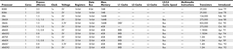


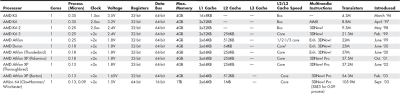
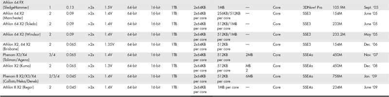
Table 3.2 AMD Processor Specifications
Data I/O Bus
Two of the more important features of a processor are the speed and width of its external data bus. These define the rate at which data can be moved into or out of the processor.
Data in a computer is sent as digital information in which certain voltages or voltage transitions occurring within specific time intervals are used to represent data as 1s and 0s. You can increase the amount of data being sent (called bandwidth) by increasing either the cycling time or the number of bits being sent at a time, or both. Over the years, processor data buses have gone from 8 bits wide to 64 bits wide. The more wires you have, the more individual bits you can send in the same time interval. All modern processors from the original Pentium and Athlon through the latest Core 2, Athlon 64 X2, and even the Itanium and Itanium 2 have a 64-bit (8-byte) wide data bus. Therefore, they can transfer 64 bits of data at a time to and from the motherboard chipset or system memory.
A good way to understand this flow of information is to consider a highway and the traffic it carries. If a highway has only one lane for each direction of travel, only one car at a time can move in a certain direction. If you want to increase the traffic flow (move more cars in a given time), you can either increase the speed of the cars (shortening the interval between them) or add more lanes, or both.
As processors evolved, more lanes were added, up to a point. You can think of an 8-bit chip as being a single-lane highway because 1 byte flows through at a time. (1 byte equals 8 individual bits.) The 16-bit chip, with 2 bytes flowing at a time, resembles a two-lane highway. You might have four lanes in each direction to move a large number of automobiles; this structure corresponds to a 32-bit data bus, which has the capability to move 4 bytes of information at a time. Taking this further, a 64-bit data bus is like having an eight-lane highway moving data in and out of the chip.
Once 64-bit-wide buses were reached, chip designers found that they couldn’t increase speed further, because it was too hard to manage synchronizing all 64 bits. It was discovered that by going back to fewer lanes, it was possible to increase the speed of the bits (that is, shorten the cycle time) such that even greater bandwidths were possible. Because of this, many newer processors have only 4-bit or 16-bit-wide data buses, and yet they have higher bandwidths than the 64-bit buses they replaced.
Another improvement in newer processors is the use of multiple separate buses for different tasks. Traditional processor design had all the data going through a single bus, whereas newer processors have separate physical buses for data to and from the chipset, memory, and graphics card slot(s).
Address Bus
The address bus is the set of wires that carries the addressing information used to describe the memory location to which the data is being sent or from which the data is being retrieved. As with the data bus, each wire in an address bus carries a single bit of information. This single bit is a single digit in the address. The more wires (digits) used in calculating these addresses, the greater the total number of address locations. The size (or width) of the address bus indicates the maximum amount of RAM a chip can address.
The highway analogy in the “Data I/O Bus” section can be used to show how the address bus fits in. If the data bus is the highway and the size of the data bus is equivalent to the number of lanes, the address bus relates to the house number or street address. The size of the address bus is equivalent to the number of digits in the house address number. For example, if you live on a street in which the address is limited to a two-digit (base 10) number, no more than 100 distinct addresses (00–99) can exist for that street (102). Add another digit, and the number of available addresses increases to 1,000 (000–999), or 103.
Computers use the binary (base 2) numbering system, so a two-digit number provides only four unique addresses (00, 01, 10, and 11), calculated as 22. A three-digit number provides only eight addresses (000—111), which is 23. For example, the 8086 and 8088 processors use a 20-bit address bus that calculates a maximum of 220, or 1,048,576 bytes (1MB), of address locations. Table 3.3 describes the memory-addressing capabilities of processors.
Table 3.3 Processor Physical Memory-Addressing Capabilities

The data bus and address bus are independent, and chip designers can use whatever size they want for each. Usually, however, chips with larger data buses have larger address buses. The sizes of the buses can provide important information about a chip’s relative power, measured in two important ways. The size of the data bus is an indication of the chip’s information-moving capability, and the size of the address bus tells you how much memory the chip can handle.
Internal Registers (Internal Data Bus)
The size of the internal registers indicates how much information the processor can operate on at one time and how it moves data around internally within the chip. This is sometimes also referred to as the internal data bus. A register is a holding cell within the processor; for example, the processor can add numbers in two different registers, storing the result in a third register. The register size determines the size of data on which the processor can operate. The register size also describes the type of software or commands and instructions a chip can run. That is, processors with 32-bit internal registers can run 32-bit instructions that are processing 32-bit chunks of data, but processors with 16-bit registers can’t. Processors from the 386 to the Pentium 4 use 32-bit internal registers and can therefore all run essentially the same 32-bit operating systems and software. The Core 2, Athlon 64, and newer processors have both 32-bit and 64-bit internal registers, which can run existing 32-bit OS and applications as well as newer 64-bit versions.
Processor Modes
All Intel and Intel-compatible processors from the 386 on up can run in several modes. Processor modes refer to the various operating environments and affect the instructions and capabilities of the chip. The processor mode controls how the processor sees and manages the system memory and the tasks that use it.
Table 3.4 summarizes the processor modes and submodes.
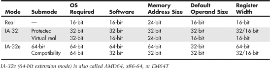
Real Mode
Real mode is sometimes called 8086 mode because it is based on the 8086 and 8088 processors. The original IBM PC included an 8088 processor that could execute 16-bit instructions using 16-bit internal registers and could address only 1MB of memory using 20 address lines. All original PC software was created to work with this chip and was designed around the 16-bit instruction set and 1MB memory model. For example, DOS and all DOS software, Windows 1.x through 3.x, and all Windows 1.x through 3.x applications are written using 16-bit instructions. These 16-bit operating systems and applications are designed to run on an original 8088 processor.
![]() See “Internal Registers (Internal Data Bus),” p. 44 (this chapter).
See “Internal Registers (Internal Data Bus),” p. 44 (this chapter).
![]() See “Address Bus,” p. 43 (this chapter).
See “Address Bus,” p. 43 (this chapter).
Later processors such as the 286 could also run the same 16-bit instructions as the original 8088, but much faster. In other words, the 286 was fully compatible with the original 8088 and could run all 16-bit software just the same as an 8088, but, of course, that software would run faster. The 16-bit instruction mode of the 8088 and 286 processors has become known as real mode. All software running in real mode must use only 16-bit instructions and live within the 20-bit (1MB) memory architecture it supports. Software of this type is usually single-tasking—that is, only one program can run at a time. No built-in protection exists to keep one program from overwriting another program or even the operating system in memory. Therefore, if more than one program is running, one of them could bring the entire system to a crashing halt.
IA-32 Mode (32-Bit)
The came the 386, which was the PC industry’s first 32-bit processor. This chip could run an entirely new 32-bit instruction set. To take full advantage of the 32-bit instruction set, a 32-bit operating system and a 32-bit application were required. This new 32-bit mode was referred to as protected mode, which alludes to the fact that software programs running in that mode are protected from overwriting one another in memory. Such protection helps make the system much more crash-proof because an errant program can’t very easily damage other programs or the operating system. In addition, a crashed program can be terminated while the rest of the system continues to run unaffected.
Knowing that new operating systems and applications—which take advantage of the 32-bit protected mode—would take some time to develop, Intel wisely built a backward-compatible real mode into the 386. That enabled it to run unmodified 16-bit operating systems and applications. It ran them quite well—much more quickly than any previous chip. For most people, that was enough. They did not necessarily want any new 32-bit software; they just wanted their existing 16-bit software to run more quickly. Unfortunately, that meant the chip was never running in the 32-bit protected mode, and all the features of that capability were being ignored.
When a 386 or later processor is running DOS (real mode), it acts like a “Turbo 8088,” which means the processor has the advantage of speed in running any 16-bit programs; it otherwise can use only the 16-bit instructions and access memory within the same 1MB memory map of the original 8088. Therefore, if you have a system with a current 32-bit or 64-bit processor running Windows 3.x or DOS, you are effectively using only the first megabyte of memory, leaving all of the other RAM largely unused!
New operating systems and applications that ran in the 32-bit protected mode of the modern processors were needed. Being stubborn, we as users resisted all the initial attempts at getting switched over to a 32-bit environment. It seems that people are very resistant to change and would be content with our older software running faster rather than adopting new software with new features. I’ll be the first one to admit that I was (and still am) one of those stubborn users myself!
Because of this resistance, true 32-bit operating systems took quite a while before getting a mainstream share in the PC marketplace. Windows XP was the first true 32-bit OS that became a true mainstream product, and that is primarily because Microsoft coerced us in that direction with Windows 9x/Me (which are mixed 16-bit/32-bit systems). Windows 3.x was the last 16-bit operating system, which some did not really consider a complete operating system because it ran on top of DOS.
IA-32 Virtual Real Mode
The key to the backward compatibility of the Windows 32-bit environment is the third mode in the processor: virtual real mode. Virtual real is essentially a virtual real mode 16-bit environment that runs inside 32-bit protected mode. When you run a DOS prompt window inside Windows, you have created a virtual real mode session. Because protected mode enables true multitasking, you can actually have several real mode sessions running, each with its own software running on a virtual PC. These can all run simultaneously, even while other 32-bit applications are running.
Note that any program running in a virtual real mode window can access up to only 1MB of memory, which that program will believe is the first and only megabyte of memory in the system. In other words, if you run a DOS application in a virtual real window, it will have a 640KB limitation on memory usage. That is because there is only 1MB of total RAM in a 16-bit environment and the upper 384KB is reserved for system use. The virtual real window fully emulates an 8088 environment, so that aside from speed, the software runs as if it were on an original real mode–only PC. Each virtual machine gets its own 1MB address space, an image of the real hardware BIOS routines, and emulation of all other registers and features found in real mode.
Virtual real mode is used when you use a DOS window to run a DOS or Windows 3.x 16-bit program. When you start a DOS application, Windows creates a virtual DOS machine under which it can run.
One interesting thing to note is that all Intel and Intel-compatible (such as AMD and VIA/Cyrix) processors power up in real mode. If you load a 32-bit operating system, it automatically switches the processor into 32-bit mode and takes control from there.
It’s also important to note that some 16-bit (DOS and Windows 3.x) applications misbehave in a 32-bit environment, which means they do things that even virtual real mode does not support. Diagnostics software is a perfect example of this. Such software does not run properly in a real mode (virtual real) window under Windows. In that case, you can still run your modern system in the original no-frills real mode by booting to a DOS or Windows 9x/Me startup floppy.
Although real mode is used by 16-bit DOS and “standard” DOS applications, special programs are available that “extend” DOS and allow access to extended memory (over 1MB). These are sometimes called DOS extenders and usually are included as part of any DOS or Windows 3.x software that uses them. The protocol that describes how to make DOS work in protected mode is called DOS protected mode interface (DPMI).
DPMI was used by Windows 3.x to access extended memory for use with Windows 3.x applications. It allowed these programs to use more memory even though they were still 16-bit programs. DOS extenders are especially popular in DOS games because they enable them to access much more of the system memory than the standard 1MB most real mode programs can address. These DOS extenders work by switching the processor in and out of real mode. In the case of those that run under Windows, they use the DPMI interface built into Windows, enabling them to share a portion of the system’s extended memory.
Another exception in real mode is that the first 64KB of extended memory is actually accessible to the PC in real mode, despite the fact that it’s not supposed to be possible. This is the result of a bug in the original IBM AT with respect to the 21st memory address line, known as A20 (A0 is the first address line). By manipulating the A20 line, real mode software can gain access to the first 64KB of extended memory—the first 64KB of memory past the first megabyte. This area of memory is called the high memory area (HMA).
IA-32e 64-Bit Extension Mode (AMD64, x86-64, EM64T)
64-bit extension mode is an enhancement to the IA-32 architecture originally designed by AMD and later adopted by Intel.
In 2003, AMD introduced the first 64-bit processor for x86-compatible desktop computers—the Athlon 64—followed by its first 64-bit server processor, the Opteron. In 2004, Intel introduced a series of 64-bit-enabled versions of its Pentium 4 desktop processor. The years that followed saw both companies introducing more and more processors with 64-bit capabilities.
Processors with 64-bit extension technology can run in real (8086) mode, IA-32 mode, or IA-32e mode. IA-32 mode enables the processor to run in protected mode and virtual real mode. IA-32e mode allows the processor to run in 64-bit mode and compatibility mode, which means you can run both 64-bit and 32-bit applications simultaneously. IA-32e mode includes two submodes:
• 64-bit mode—Enables a 64-bit operating system to run 64-bit applications
• Compatibility mode—Enables a 64-bit operating system to run most existing 32-bit software
IA-32e 64-bit mode is enabled by loading a 64-bit operating system and is used by 64-bit applications. In the 64-bit submode, the following new features are available:
• 64-bit linear memory addressing
• Physical memory support beyond 4GB (limited by the specific processor)
• Eight new general-purpose registers (GPRs)
• Eight new registers for streaming SIMD extensions (MMX, SSE, SSE2, and SSE3)
• 64-bit-wide GPRs and instruction pointers
IE-32e compatibility mode enables 32-bit and 16-bit applications to run under a 64-bit operating system. Unfortunately, legacy 16-bit programs that run in virtual real mode (that is, DOS programs) are not supported and will not run, which is likely to be the biggest problem for many users. Similar to 64-bit mode, compatibility mode is enabled by the operating system on an individual code basis, which means 64-bit applications running in 64-bit mode can operate simultaneously with 32-bit applications running in compatibility mode.
What we need to make all this work is a 64-bit operating system and, more importantly, 64-bit drivers for all our hardware to work under that OS. Although Microsoft released a 64-bit version of Windows XP, few companies released 64-bit XP drivers. It wasn’t until Windows Vista and especially Windows 7 x64 versions were released that 64-bit drivers became plentiful enough that 64-bit hardware support was considered mainstream.
Note that Microsoft uses the term x64 to refer to processors that support either AMD64 or EM64T because AMD and Intel’s extensions to the standard IA32 architecture are practically identical and can be supported with a single version of Windows.
Note
Early versions of EM64T-equipped processors from Intel lacked support for the LAHF and SAHF instructions used in the AMD64 instruction set. However, Pentium 4 and Xeon DP processors using core steppings G1 and higher completely support these instructions; a BIOS update is also needed. Newer multicore processors with 64-bit support include these instructions as well.
The physical memory limits for Windows XP and later 32-bit and 64-bit editions are shown in Table 3.5.
Table 3.5 Windows Physical Memory Limits

The major difference between 32-bit and 64-bit Windows is memory support, specifically breaking the 4GB barrier found in 32-bit Windows systems. 32-bit versions of Windows support up to 4GB of physical memory, with up to 2GB of dedicated memory per process. 64-bit versions of Windows support up to 192GB of physical memory, with up to 4GB for each 32-bit process and up to 8TB for each 64-bit process. Support for more memory means applications can preload more data into memory, which the processor can access much more quickly.
64-bit Windows runs 32-bit Windows applications with no problems, but it does not run 16-bit Windows or DOS applications, or any other programs that run in virtual real mode. Also, drivers are another big problem. 32-bit processes cannot load 64-bit dynamic link libraries (DLLs), and 64-bit processes cannot load 32-bit DLLs. This essentially means that, for all the devices you have connected to your system, you need both 32-bit and 64-bit drivers for them to work. Acquiring 64-bit drivers for older devices or devices that are no longer supported can be difficult or impossible. Before installing a 64-bit version of Windows, be sure to check with the vendors of your internal and add-on hardware for 64-bit drivers.
You should keep all the memory size, software, and driver issues in mind when considering the transition from 32-bit to 64-bit technology. The transition from 32-bit hardware to mainstream 32-bit computing took 16 years. The first 64-bit PC processor was released in 2003, and 64-bit computing really didn’t become mainstream until the release of Windows 7 in late 2009.
Processor Benchmarks
People love to know how fast (or slow) their computers are. We have always been interested in speed; it is human nature. To help us with this quest, various benchmark test programs can be used to measure different aspects of processor and system performance. Although no single numerical measurement can completely describe the performance of a complex device such as a processor or a complete PC, benchmarks can be useful tools for comparing different components and systems.
However, the only truly accurate way to measure your system’s performance is to test the system using the actual software applications you use. Although you think you might be testing one component of a system, often other parts of the system can have an effect. It is inaccurate to compare systems with different processors, for example, if they also have different amounts or types of memory, different hard disks, video cards, and so on. All these things and more will skew the test results.
Benchmarks can typically be divided into two types: component or system tests. Component benchmarks measure the performance of specific parts of a computer system, such as a processor, hard disk, video card, or optical drive, whereas system benchmarks typically measure the performance of the entire computer system running a given application or test suite. These are also often called synthetic benchmarks because they don’t measure any actual work.
Benchmarks are, at most, only one kind of information you can use during the upgrading or purchasing process. You are best served by testing the system using your own set of software operating systems and applications and in the configuration you will be running.
I normally recommend using application-based benchmarks such as the BAPCo SYSmark (www.bapco.com) to measure the relative performance difference between different processors and/or systems. The next section includes tables that show the results of SYSmark benchmark tests on current as well as older processors.
Comparing Processor Performance
A common misunderstanding about processors is their different speed ratings. This section covers processor speed in general and then provides more specific information about Intel, AMD, and VIA/Cyrix processors.
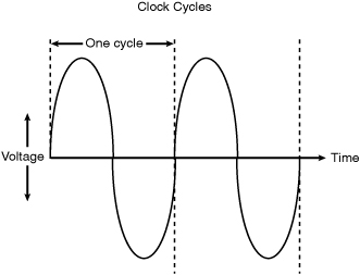
A computer system’s clock speed is measured as a frequency, usually expressed as a number of cycles per second. A crystal oscillator controls clock speeds using a sliver of quartz sometimes housed in what looks like a small tin container. Newer systems include the oscillator circuitry in the motherboard chipset, so it might not be a visible separate component on newer boards. As voltage is applied to the quartz, it begins to vibrate (oscillate) at a harmonic rate dictated by the shape and size of the crystal (sliver). The oscillations emanate from the crystal in the form of a current that alternates at the harmonic rate of the crystal. This alternating current is the clock signal that forms the time base on which the computer operates. A typical computer system runs millions or billions of these cycles per second, so speed is measured in megahertz or gigahertz. (One hertz is equal to one cycle per second.) An alternating current signal is like a sine wave, with the time between the peaks of each wave defining the frequency (see Figure 3.1).
Figure 3.1 Alternating current signal showing clock cycle timing.
Note
The hertz was named for the German physicist Heinrich Rudolf Hertz. In 1885, Hertz confirmed the electromagnetic theory, which states that light is a form of electromagnetic radiation and is propagated as waves.
A single cycle is the smallest element of time for the processor. Every action requires at least one cycle and usually multiple cycles. To transfer data to and from memory, for example, a modern processor such as the Pentium 4 needs a minimum of three cycles to set up the first memory transfer and then only a single cycle per transfer for the next three to six consecutive transfers. The extra cycles on the first transfer typically are called wait states. A wait state is a clock tick in which nothing happens. This ensures that the processor isn’t getting ahead of the rest of the computer.
![]() See “SIMMs, DIMMs, and RIMMs,” p. 397 (Chapter 6, “Memory”).
See “SIMMs, DIMMs, and RIMMs,” p. 397 (Chapter 6, “Memory”).
The time required to execute instructions also varies:
• 8086 and 8088—The original 8086 and 8088 processors take an average of 12 cycles to execute a single instruction.
• 286 and 386—The 286 and 386 processors improve this rate to about 4.5 cycles per instruction.
• 486—The 486 and most other fourth-generation Intel-compatible processors, such as the AMD 5x86, drop the rate further, to about 2 cycles per instruction.
• Pentium/K6—The Pentium architecture and other fifth-generation Intel-compatible processors, such as those from AMD and Cyrix, include twin instruction pipelines and other improvements that provide for operation at one or two instructions per cycle.
• P6/P7 and newer—Sixth-, seventh-, and newer-generation processors can execute as many as three or more instructions per cycle, with multiples of that possible on multicore processors.
Different instruction execution times (in cycles) make comparing systems based purely on clock speed or number of cycles per second difficult. How can two processors that run at the same clock rate perform differently with one running “faster” than the other? The answer is simple: efficiency.
The main reason the 486 was considered fast relative to a 386 is that it executes twice as many instructions in the same number of cycles. The same thing is true for a Pentium; it executes about twice as many instructions in a given number of cycles as a 486. Therefore, given the same clock speed, a Pentium is twice as fast as a 486, and consequently a 133MHz 486 class processor (such as the AMD 5x86-133) is not even as fast as a 75MHz Pentium! That is because Pentium megahertz are “worth” about double what 486 megahertz are worth in terms of instructions completed per cycle. The Pentium II and III are about 50% faster than an equivalent Pentium at a given clock speed because they can execute about that many more instructions in the same number of cycles.
Unfortunately, after the Pentium III, it becomes much more difficult to compare processors on clock speed alone. This is because the different internal architectures make some processors more efficient than others, but these same efficiency differences result in circuitry that is capable of running at different maximum speeds. The less efficient the circuit, the higher the clock speed it can attain, and vice versa.
One of the biggest factors in efficiency is the number of stages in the processor’s internal pipeline (see Table 3.6).
Table 3.6 Number of Pipelines per CPU

A deeper pipeline effectively breaks instructions down into smaller microsteps, which allows overall higher clock rates to be achieved using the same silicon technology. However, this also means that overall fewer instructions can be executed in a single cycle as compared to processors with shorter pipelines. This is because, if a branch prediction or speculative execution step fails (which happens fairly frequently inside the processor as it attempts to line up instructions in advance), the entire pipeline has to be flushed and refilled. Thus, if you compared an Intel Core i7 or AMD Phenom to a Pentium 4 running at the same clock speed, the Core i7 and Phenom would execute more instructions in the same number of cycles.
Although it is a disadvantage to have a deeper pipeline in terms of instruction efficiency, processors with deeper pipelines can run at higher clock rates on a given manufacturing technology. Thus, even though a deeper pipeline might be less efficient, the higher resulting clock speeds can make up for it. The deeper 20- or 31-stage pipeline in the P4 architecture enabled significantly higher clock speeds to be achieved using the same silicon die process as other chips. As an example, the 0.13-micron process Pentium 4 ran up to 3.4GHz while the Athlon XP topped out at 2.2GHz (3200+ model) in the same introduction timeframe. Even though the Pentium 4 executes fewer instructions in each cycle, the overall higher cycling speeds made up for the loss of efficiency—the higher clock speed versus the more efficient processing effectively cancelled each other out.
Unfortunately, the deep pipeline combined with high clock rates did come with a penalty in power consumption, and therefore heat generation as well. Eventually it was determined that the power penalty was too great, causing Intel to drop back to a more efficient design in its newer Core microarchitecture processors. Rather than solely increase clock rates, performance was increased by combining multiple processors into a single chip, thus improving the effective instruction efficiency even further. This began the push toward multicore processors.
One thing is clear in all of this confusion: Raw clock speed is not a good way to compare chips, unless they are from the same manufacturer, model, and family.
To fairly compare various CPUs at different clock speeds, Intel originally devised a specific series of benchmarks called the iCOMP (Intel Comparative Microprocessor Performance) index. The iCOMP index benchmark was released in original iCOMP, iCOMP 2.0, and iCOMP 3.0 versions.
The iCOMP 2.0 index was derived from several independent benchmarks as an indication of relative processor performance. The benchmarks balance integer with floating-point and multimedia performance.
Table 3.7 shows the relative power, or iCOMP 2.0 index, for several older Intel processors.
Table 3.7 Intel iCOMP 2.0 Index Ratings

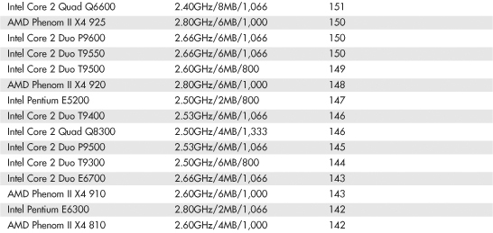
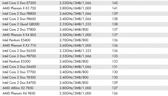
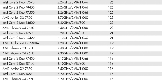
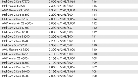
Intel and AMD rate their latest processors using the commercially available BAPCo SYSmark benchmark suites. SYSmark is an application-based benchmark that runs various scripts to do actual work using popular applications. It is used by many companies for testing and comparing PC systems and components. The SYSmark benchmark is a much more modern and real-world benchmark than the iCOMP benchmark Intel previously used, and because it is available to anybody, the results can be independently verified. The SYSmark benchmark software can be purchased from BAPCo at www.bapco.com or from FutureMark at www.futuremark.com. The ratings for the various processors under these benchmark suites are shown in Tables 3.8, 3.9, and 3.10.
Table 3.8 SYSmark 2004 Scores for Various Processors


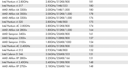

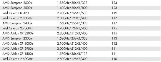
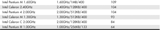
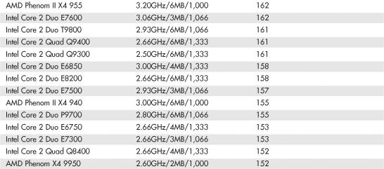
Table 3.9 SYSmark 2004 SE Scores for Various Processors

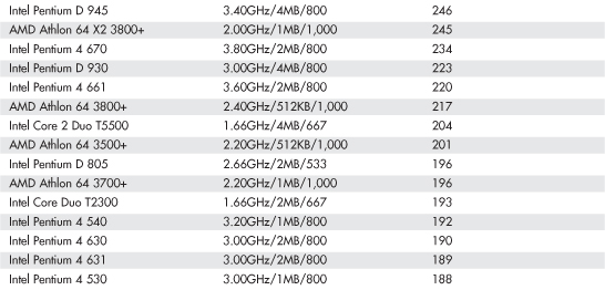
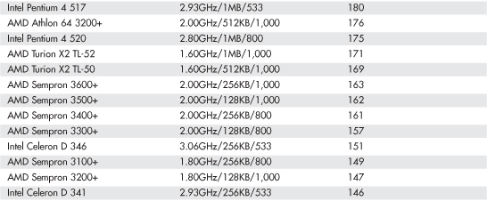
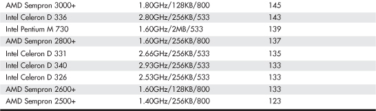
Table 3.10 SYSmark 2007 Preview Scores for Various Processors


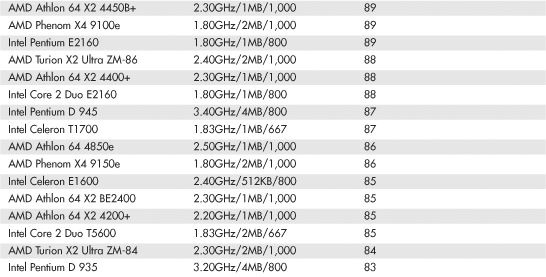


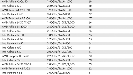

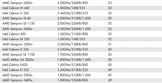

The SYSmark benchmarks are commercially available application-based benchmarks that reflect the normal usage of business users employing modern Internet content creation and office applications. However, it is important to note that the scores listed here are produced by complete systems and are affected by things such as the specific version of the processor, the motherboard and chipset used, the amount and type of memory installed, the speed of the hard disk, and other factors. For complete disclosure of the other factors resulting in the given scores, see the full disclosure reports on the BAPCo website at www.bapco.com.
Cache Memory
As processor core speeds increased, memory speeds could not keep up. How could you run a processor faster than the memory from which you feed it without having performance suffer terribly? The answer was cache. In its simplest terms, cache memory is a high-speed memory buffer that temporarily stores data the processor needs, allowing the processor to retrieve that data faster than if it came from main memory. But there is one additional feature of a cache over a simple buffer, and that is intelligence. A cache is a buffer with a brain.
A buffer holds random data, usually on a first in, first out basis or a first in, last out basis. A cache, on the other hand, holds the data the processor is most likely to need in advance of it actually being needed. This enables the processor to continue working at either full speed or close to it without having to wait for the data to be retrieved from slower main memory. Cache memory is usually made up of static RAM (SRAM) memory integrated into the processor die, although older systems with cache also used chips installed on the motherboard.
![]() See “Cache Memory: SRAM,” p. 379 (Chapter 6).
See “Cache Memory: SRAM,” p. 379 (Chapter 6).
For the vast majority of desktop systems, there are two levels of processor/memory cache used in a modern PC: Level 1 (L1) and Level 2 (L2). Some processors also have Level 3 cache; however, this is rare. These caches and how they function are described in the following sections.
Internal Level 1 Cache
All modern processors starting with the 486 family include an integrated L1 cache and controller. The integrated L1 cache size varies from processor to processor, starting at 8KB for the original 486DX and now up to 32KB, 64KB, or more in the latest processors.
To understand the importance of cache, you need to know the relative speeds of processors and memory. The problem with this is that processor speed usually is expressed in MHz or GHz (millions or billions of cycles per second), whereas memory speeds are often expressed in nanoseconds (billionths of a second per cycle). Most newer types of memory express the speed in either MHz or in megabyte per second (MBps) bandwidth (throughput).
Both are really time- or frequency-based measurements, and a chart comparing them can be found in Table 6.3 in Chapter 6. In this table, you will note that a 233MHz processor equates to 4.3-nanosecond cycling, which means you would need 4ns memory to keep pace with a 200MHz CPU. Also note that the motherboard of a 233MHz system typically runs at 66MHz, which corresponds to a speed of 15ns per cycle and requires 15ns memory to keep pace. Finally, note that 60ns main memory (common on many Pentium-class systems) equates to a clock speed of approximately 16MHz. So, a typical Pentium 233 system has a processor running at 233MHz (4.3ns per cycle), a motherboard running at 66MHz (15ns per cycle), and main memory running at 16MHz (60ns per cycle). This might seem like a rather dated example, but in a moment, you will see that the figures listed here make it easy for me to explain how cache memory works.
Because L1 cache is always built into the processor die, it runs at the full-core speed of the processor internally. By full-core speed, I mean this cache runs at the higher clock multiplied internal processor speed rather than the external motherboard speed. This cache basically is an area of very fast memory built into the processor and is used to hold some of the current working set of code and data. Cache memory can be accessed with no wait states because it is running at the same speed as the processor core.
Using cache memory reduces a traditional system bottleneck because system RAM is almost always much slower than the CPU; the performance difference between memory and CPU speed has become especially large in recent systems. Using cache memory prevents the processor from having to wait for code and data from much slower main memory, thus improving performance. Without the L1 cache, a processor would frequently be forced to wait until system memory caught up.
Cache is even more important in modern processors because it is often the only memory in the entire system that can truly keep up with the chip. Most modern processors are clock multiplied, which means they are running at a speed that is really a multiple of the motherboard into which they are plugged. The only types of memory matching the full speed of the processor are the L1, L2, and maybe L3 caches built into the processor core.
![]() See “Memory Module Speed,” p. 413 (Chapter 6).
See “Memory Module Speed,” p. 413 (Chapter 6).
If the data the processor wants is already in the internal cache, the CPU does not have to wait. If the data is not in the cache, the CPU must fetch it from the Level 2 cache or (in less sophisticated system designs) from the system bus, meaning main memory directly.
How Cache Works
To learn how the L1 cache works, consider the following analogy.
This story involves a person (in this case, you) eating food to act as the processor requesting and operating on data from memory. The kitchen where the food is prepared is the main system memory (typically DDR, DDR2, or DDR3 DIMMs). The cache controller is the waiter, and the L1 cache is the table at which you are seated.
Okay, here’s the story. Say you start to eat at a particular restaurant every day at the same time. You come in, sit down, and order a hot dog. To keep this story proportionately accurate, let’s say you normally eat at the rate of one bite (byte? <g>) every four seconds (233MHz = about 4ns cycling). It also takes 60 seconds for the kitchen to produce any given item that you order (60ns main memory).
So, when you first arrive, you sit down, order a hot dog, and you have to wait for 60 seconds for the food to be produced before you can begin eating. After the waiter brings the food, you start eating at your normal rate. Pretty quickly you finish the hot dog, so you call the waiter over and order a hamburger. Again you wait 60 seconds while the hamburger is being produced. When it arrives, you again begin eating at full speed. After you finish the hamburger, you order a plate of fries. Again you wait, and after it is delivered 60 seconds later, you eat it at full speed. Finally, you decide to finish the meal and order cheesecake for dessert. After another 60-second wait, you can eat cheesecake at full speed. Your overall eating experience consists of mostly a lot of waiting, followed by short bursts of actual eating at full speed.
After coming into the restaurant for two consecutive nights at exactly 6 p.m. and ordering the same items in the same order each time, on the third night the waiter begins to think, “I know this guy is going to be here at 6 p.m., order a hot dog, a hamburger, fries, and then cheesecake. Why don’t I have these items prepared in advance and surprise him? Maybe I’ll get a big tip.” So you enter the restaurant and order a hot dog, and the waiter immediately puts it on your plate, with no waiting! You then proceed to finish the hot dog and right as you are about to request the hamburger, the waiter deposits one on your plate. The rest of the meal continues in the same fashion, and you eat the entire meal, taking a bite every four seconds, and never have to wait for the kitchen to prepare the food. Your overall eating experience this time consists of all eating, with no waiting for the food to be prepared, due primarily to the intelligence and thoughtfulness of your waiter.
This analogy exactly describes the function of the L1 cache in the processor. The L1 cache itself is a table that can contain one or more plates of food. Without a waiter, the space on the table is a simple food buffer. When it’s stocked, you can eat until the buffer is empty, but nobody seems to be intelligently refilling it. The waiter is the cache controller who takes action and adds the intelligence to decide which dishes are to be placed on the table in advance of your needing them. Like the real cache controller, he uses his skills to literally guess which food you will require next, and if and when he guesses right, you never have to wait.
Let’s now say on the fourth night you arrive exactly on time and start off with the usual hot dog. The waiter, by now really feeling confident, has the hot dog already prepared when you arrive, so there is no waiting.
Just as you finish the hot dog, and right as he is placing a hamburger on your plate, you say “Gee, I’d really like a bratwurst now; I didn’t actually order this hamburger.” The waiter guessed wrong, and the consequence is that this time you have to wait the full 60 seconds as the kitchen prepares your brat. This is known as a cache miss, in which the cache controller did not correctly fill the cache with the data the processor actually needed next. The result is waiting, or in the case of a sample 233MHz Pentium system, the system essentially throttles back to 16MHz (RAM speed) whenever a cache miss occurs.
According to Intel, the L1 cache in most of its processors has approximately a 90% hit ratio (some processors, such as the Pentium 4, are slightly higher). This means that the cache has the correct data 90% of the time, and consequently the processor runs at full speed (233MHz in this example) 90% of the time. However, 10% of the time the cache controller guesses wrong and the data has to be retrieved out of the significantly slower main memory, meaning the processor has to wait. This essentially throttles the system back to RAM speed, which in this example was 60ns or 16MHz.
In this analogy, the processor was 14 times faster than the main memory. Memory speeds have increased from 16MHz (60ns) to 333MHz (3.0ns) or faster in the latest systems, but processor speeds have also risen to 3GHz and beyond, so even in the latest systems, memory is still 7.5 or more times slower than the processor. Cache is what makes up the difference.
The main feature of L1 cache is that it has always been integrated into the processor core, where it runs at the same speed as the core. This, combined with the hit ratio of 90% or greater, makes L1 cache very important for system performance.
Level 2 Cache
To mitigate the dramatic slowdown every time an L1 cache miss occurs, a secondary (L2) cache is employed.
Using the restaurant analogy I used to explain L1 cache in the previous section, I’ll equate the L2 cache to a cart of additional food items placed strategically in the restaurant such that the waiter can retrieve food from the cart in only 15 seconds (versus 60 seconds from the kitchen). In an actual Pentium class (Socket 7) system, the L2 cache is mounted on the motherboard, which means it runs at motherboard speed (66MHz, or 15ns in this example). Now, if you ask for an item the waiter did not bring in advance to your table, instead of making the long trek back to the kitchen to retrieve the food and bring it back to you 60 seconds later, he can first check the cart where he has placed additional items. If the requested item is there, he will return with it in only 15 seconds. The net effect in the real system is that instead of slowing down from 233MHz to 16MHz waiting for the data to come from the 60ns main memory, the system can instead retrieve the data from the 15ns (66MHz) L2 cache. The effect is that the system slows down from 233MHz to 66MHz.
All modern processors have integrated L2 cache that runs at the same speed as the processor core, which is also the same speed as the L1 cache. For the analogy to describe these newer chips, the waiter would simply place the cart right next to the table you were seated at in the restaurant. Then, if the food you desired wasn’t on the table (L1 cache miss), it would merely take a longer reach over to the adjacent L2 cache (the cart, in this analogy) rather than a 15-second walk to the cart as with the older designs.
Level 3 Cache
A few processors, primarily those designed for very high-performance desktop operation or enterprise-level servers, contain a third level of cache known as L3 cache. In the past relatively few processors had L3 cache, but it is becoming more and more common in newer and faster multicore processors such as the Intel Core and AMD Phenom processors.
Extending the restaurant analogy I used to explain L1 and L2 caches, I’ll equate L3 cache to another cart of additional food items placed in the restaurant next to the cart used to symbolize L2 cache. If the food item needed was not on the table (L1 cache miss) or on the first food cart (L2 cache miss), the waiter could then reach over to the second food cart to retrieve a necessary item.
L3 cache proves especially useful in multicore processors, where the L3 is generally shared among all the cores. Although currently a sign of a high-end chip, future mainstream processors will include L3 cache as a standard feature.
Cache Performance and Design
Just as with the L1 cache, most L2 caches have a hit ratio also in the 90% range; therefore, if you look at the system as a whole, 90% of the time it will be running at full speed (233MHz in this example) by retrieving data out of the L1 cache. Ten percent of the time it will slow down to retrieve the data from the L2 cache. Ninety percent of the time the processor goes to the L2 cache, the data will be in the L2, and 10% of that time it will have to go to the slow main memory to get the data because of an L2 cache miss. So, by combining both caches, our sample system runs at full processor speed 90% of the time (233MHz in this case), at motherboard speed 9% (90% of 10%) of the time (66MHz in this case), and at RAM speed about 1% (10% of 10%) of the time (16MHz in this case). You can clearly see the importance of both the L1 and L2 caches; without them the system uses main memory more often, which is significantly slower than the processor.
This brings up other interesting points. If you could spend money doubling the performance of either the main memory (RAM) or the L2 cache, which would you improve? Considering that main memory is used directly only about 1% of the time, if you doubled performance there, you would double the speed of your system only 1% of the time! That doesn’t sound like enough of an improvement to justify much expense. On the other hand, if you doubled L2 cache performance, you would be doubling system performance 9% of the time, a much greater improvement overall. I’d much rather improve L2 than RAM performance.
The processor and system designers at Intel and AMD know this and have devised methods of improving the performance of L2 cache. In Pentium (P5) class systems, the L2 cache usually was found on the motherboard and had to therefore run at motherboard speed. Intel made the first dramatic improvement by migrating the L2 cache from the motherboard directly into the processor and initially running it at the same speed as the main processor. The cache chips were made by Intel and mounted next to the main processor die in a single chip housing. This proved too expensive, so with the Pentium II, Intel began using cache chips from third-party suppliers such as Sony, Toshiba, NEC, Samsung, and others. Because these were supplied as complete packaged chips and not raw die, Intel mounted them on a circuit board alongside the processor. This is why the Pentium II was designed as a cartridge rather than what looked like a chip.
One problem was the speed of the available third-party cache chips. The fastest ones on the market were 3ns or higher, meaning 333MHz or less in speed. Because the processor was being driven in speed above that, in the Pentium II and initial Pentium III processors Intel had to run the L2 cache at half the processor speed because that is all the commercially available cache memory could handle. AMD followed suit with the Athlon processor, which had to drop L2 cache speed even further in some models to two-fifths or one-third the main CPU speed to keep the cache memory speed less than the 333MHz commercially available chips.
Then a breakthrough occurred, which first appeared in Celeron processors 300A and above. These had 128KB of L2 cache, but no external chips were used. Instead, the L2 cache had been integrated directly into the processor core just like the L1. Consequently, both the L1 and L2 caches now would run at full processor speed, and more importantly scale up in speed as the processor speeds increased in the future. In the newer Pentium III, as well as all the Xeon and Celeron processors, the L2 cache runs at full processor core speed, which means there is no waiting or slowing down after an L1 cache miss. AMD also achieved full-core speed on-die cache in its later Athlon and Duron chips. Using on-die cache improves performance dramatically because 9% of the time the system would be using the L2, it would now remain at full speed instead of slowing down to one-half or less the processor speed or, even worse, slow down to motherboard speed as in Socket 7 designs. Another benefit of on-die L2 cache is cost, which is less because now fewer parts are involved.
Let’s revisit the restaurant analogy using a 3.6GHz processor. You would now be taking a bite every half second (3.6GHz = 0.28ns cycling). The L1 cache would also be running at that speed, so you could eat anything on your table at that same rate (the table = L1 cache). The real jump in speed comes when you want something that isn’t already on the table (L1 cache miss), in which case the waiter reaches over to the cart (which is now directly adjacent to the table) and nine out of ten times is able to find the food you want in just over one-quarter second (L2 speed = 3.6GHz or 0.28ns cycling). In this system, you would run at 3.6GHz 99% of the time (L1 and L2 hit ratios combined) and slow down to RAM speed (wait for the kitchen) only 1% of the time, as before. With faster memory running at 800MHz (1.25ns), you would have to wait only 1.25 seconds for the food to come from the kitchen. If only restaurant performance would increase at the same rate processor performance has!
Cache Organization
You know that cache stores copies of data from various main memory addresses. Because the cache cannot hold copies of the data from all the addresses in main memory simultaneously, there has to be a way to know which addresses are currently copied into the cache so that, if we need data from those addresses, it can be read from the cache rather than from the main memory. This function is performed by Tag RAM, which is additional memory in the cache that holds an index of the addresses that are copied into the cache. Each line of cache memory has a corresponding address tag that stores the main memory address of the data currently copied into that particular cache line. If data from a particular main memory address is needed, the cache controller can quickly search the address tags to see whether the requested address is currently being stored in the cache (a hit) or not (a miss). If the data is there, it can be read from the faster cache; if it isn’t, it has to be read from the much slower main memory.
Various ways of organizing or mapping the tags affect how cache works. A cache can be mapped as fully associative, direct-mapped, or set associative.
In a fully associative mapped cache, when a request is made for data from a specific main memory address, the address is compared against all the address tag entries in the cache tag RAM. If the requested main memory address is found in the tag (a hit), the corresponding location in the cache is returned. If the requested address is not found in the address tag entries, a miss occurs and the data must be retrieved from the main memory address instead of the cache.
In a direct-mapped cache, specific main memory addresses are preassigned to specific line locations in the cache where they will be stored. Therefore, the tag RAM can use fewer bits because when you know which main memory address you want, only one address tag needs to be checked and each tag needs to store only the possible addresses a given line can contain. This also results in faster operation because only one tag address needs to be checked for a given memory address.
A set associative cache is a modified direct-mapped cache. A direct-mapped cache has only one set of memory associations, meaning a given memory address can be mapped into (or associated with) only a specific given cache line location. A two-way set associative cache has two sets, so that a given memory location can be in one of two locations. A four-way set associative cache can store a given memory address into four different cache line locations (or sets). By increasing the set associativity, the chance of finding a value increases; however, it takes a little longer because more tag addresses must be checked when searching for a specific location in the cache. In essence, each set in an n-way set associative cache is a subcache that has associations with each main memory address. As the number of subcaches or sets increases, eventually the cache becomes fully associative—a situation in which any memory address can be stored in any cache line location. In that case, an n-way set associative cache is a compromise between a fully associative cache and a direct-mapped cache.
In general, a direct-mapped cache is the fastest at locating and retrieving data from the cache because it has to look at only one specific tag address for a given memory address. However, it also results in more misses overall than the other designs. A fully associative cache offers the highest hit ratio but is the slowest at locating and retrieving the data because it has many more address tags to check through. An n-way set associative cache is a compromise between optimizing cache speed and hit ratio, but the more associativity there is, the more hardware (tag bits, comparator circuits, and so on) is required, making the cache more expensive. Obviously, cache design is a series of tradeoffs, and what works best in one instance might not work best in another. Multitasking environments such as Windows are good examples of environments in which the processor needs to operate on different areas of memory simultaneously and in which an n-way cache can improve performance.
The contents of the cache must always be in sync with the contents of main memory to ensure that the processor is working with current data. For this reason, the internal cache in the 486 family was a write-through cache. Write-through means that when the processor writes information out to the cache, that information is automatically written through to main memory as well.
By comparison, Pentium and later chips have an internal write-back cache, which means that both reads and writes are cached, further improving performance.
Another feature of improved cache designs is that they are nonblocking. This is a technique for reducing or hiding memory delays by exploiting the overlap of processor operations with data accesses. A nonblocking cache enables program execution to proceed concurrently with cache misses as long as certain dependency constraints are observed. In other words, the cache can handle a cache miss much better and enable the processor to continue doing something nondependent on the missing data.
The cache controller built into the processor also is responsible for watching the memory bus when alternative processors, known as bus masters, are in control of the system. This process of watching the bus is referred to as bus snooping. If a bus master device writes to an area of memory that also is stored in the processor cache currently, the cache contents and memory no longer agree. The cache controller then marks this data as invalid and reloads the cache during the next memory access, preserving the integrity of the system.
All PC processor designs that support cache memory include a feature known as a translation lookaside buffer (TLB) to improve recovery from cache misses. The TLB is a table inside the processor that stores information about the location of recently accessed memory addresses. The TLB speeds up the translation of virtual addresses to physical memory addresses. To improve TLB performance, several recent processors have increased the number of entries in the TLB, as AMD did when it moved from the Athlon Thunderbird core to the Palomino core. Pentium 4 processors that support HT Technology have a separate instruction TLB (iTLB) for each virtual processor thread.
![]() See “Hyper-Threading Technology,” p. 75 (this chapter).
See “Hyper-Threading Technology,” p. 75 (this chapter).
As clock speeds increase, cycle time decreases. Newer systems don’t use cache on the motherboard any longer because the faster system memory used in modern systems can keep up with the motherboard speed. Modern processors all integrate the L2 cache into the processor die just like the L1 cache, and some include on-die L3 as well. This enables the L2/L3 to run at full-core speed because it is now a part of the core. Cache speed is always more important than size. The general rule is that a smaller but faster cache is always better than a slower but bigger cache.
Processor Features
As new processors are introduced, new features are continually added to their architectures to help improve everything from performance in specific types of applications to the reliability of the CPU as a whole. The next few sections take a look at some of these technologies.
System Management Mode (SMM)
Spurred on initially by the need for more robust power management capabilities in mobile computers, Intel and AMD began adding System Management Mode (SMM) to its processors during the early ’90s. SMM is a special-purpose operating mode provided for handling low-level system power management and hardware control functions. SMM offers an isolated software environment that is transparent to the operating system or applications software, and is intended for use by system BIOS or low-level driver code.
SMM was first introduced as part of the Intel 386SL mobile processor in October 1990. SMM later appeared as part of the 486SL processor in November 1992, and in the entire 486 line starting in June 1993. SMM was notably absent from the first Pentium processors when they were released in March 1993; however, SMM was included in all 75MHz and faster Pentium processors released on or after October 1994. AMD added SMM to their enhanced Am486 and K5 processors around that time as well. All other Intel and AMD x86-based processors introduced since that time have incorporated SMM as well.
SMM is invoked by signaling a special interrupt pin on the processor, which generates a System Management Interrupt (SMI), the highest priority nonmaskable interrupt available. When SMM starts, the context or state of the processor and currently running programs are saved. Then the processor switches to a separate dedicated address space and executes the SMM code, which runs transparently to the interrupted program as well as any other software on the system. Once the SMM task is complete, a resume instruction restores the previously saved context or state of the processor and programs, and the processor resumes running exactly where it left off.
While initially used mainly for power management, SMM was designed to be used by any low-level system functions that need to function independent of the OS and other software on the system. In modern systems, this includes the following:
• ACPI and APM power management functions
• USB legacy (keyboard and mouse) support
• USB boot (drive emulation)
• Password and security functions
• Thermal monitoring
• Fan speed monitoring
• Reading/writing CMOS RAM
• BIOS updating
• Logging memory ECC errors
• Logging hardware errors besides memory
• Wake and Alert functions such as Wake On LAN (WOL)
One example of SMM in operation can be seen when the system tries to access a peripheral device that had been previously powered down to save energy. For example, say that a program makes a request to read a file on a hard drive, but the drive had previously spun down to save energy. Upon access, the host adapter generates a System Management Interrupt (SMI) to invoke System Management Mode (SMM). The SMM software then issues commands to spin up the drive and make it ready. Then SMM returns control to the OS, and the file load continues as if the drive had been spinning all along.
Superscalar Execution
The fifth-generation Pentium and newer processors feature multiple internal instruction execution pipelines, which enable them to execute multiple instructions at the same time. The 486 and all preceding chips can perform only a single instruction at a time. Intel calls the capability to execute more than one instruction at a time superscalar technology.
Superscalar architecture was initially associated with high-output Reduced Instruction Set Computer (RISC) chips. A RISC chip has a less complicated instruction set with fewer and simpler instructions. Although each instruction accomplishes less, the overall clock speed can be higher, which usually increases performance. The Pentium is one of the first Complex Instruction Set Computer (CISC) chips to be considered superscalar. A CISC chip uses a richer, fuller-featured instruction set, which has more complicated instructions. As an example, say you wanted to instruct a robot to screw in a light bulb. Using CISC instructions, you would say
1. Pick up the bulb.
2. Insert it into the socket.
3. Rotate clockwise until tight.
Using RISC instructions, you would say something more along the lines of
1. Lower hand.
2. Grasp bulb.
3. Raise hand.
4. Insert bulb into socket.
5. Rotate clockwise one turn.
6. Is bulb tight? If not, repeat step 5.
7. End.
Overall, many more RISC instructions are required to do the job because each instruction is simpler (reduced) and does less. The advantage is that there are fewer overall commands the robot (or processor) has to deal with and it can execute the individual commands more quickly, and thus in many cases execute the complete task (or program) more quickly as well. The debate goes on whether RISC or CISC is really better, but in reality there is no such thing as a pure RISC or CISC chip—it is all just a matter of definition, and the lines are somewhat arbitrary.
Intel and compatible processors have generally been regarded as CISC chips, although the fifth- and latergeneration versions have many RISC attributes and internally break CISC instructions down into RISC versions.
MMX Technology
MMX technology was originally named for multimedia extensions, or matrix math extensions, depending on whom you ask. Intel officially states that it is actually not an abbreviation and stands for nothing other than the letters MMX (not being an abbreviation was apparently required so that the letters could be trademarked); however, the internal origins are probably one of the preceding. MMX technology was introduced in the later fifth-generation Pentium processors as a kind of add-on that improves video compression/decompression, image manipulation, encryption, and I/O processing—all of which are used in a variety of today’s software.
MMX consists of two main processor architectural improvements. The first is very basic; all MMX chips have a larger internal L1 cache than their non-MMX counterparts. This improves the performance of any and all software running on the chip, regardless of whether it actually uses the MMX-specific instructions.
The other part of MMX is that it extends the processor instruction set with 57 new commands or instructions, as well as a new instruction capability called single instruction, multiple data (SIMD).
Modern multimedia and communication applications often use repetitive loops that, while occupying 10% or less of the overall application code, can account for up to 90% of the execution time. SIMD enables one instruction to perform the same function on multiple pieces of data, similar to a teacher telling an entire class to “sit down,” rather than addressing each student one at a time. SIMD enables the chip to reduce processor-intensive loops common with video, audio, graphics, and animation.
Intel also added 57 new instructions specifically designed to manipulate and process video, audio, and graphical data more efficiently. These instructions are oriented to the highly parallel and often repetitive sequences frequently found in multimedia operations. Highly parallel refers to the fact that the same processing is done on many data points, such as when modifying a graphic image. The main drawbacks to MMX were that it worked only on integer values and used the floating-point unit for processing, so time was lost when a shift to floating-point operations was necessary. These drawbacks were corrected in the additions to MMX from Intel and AMD.
Intel licensed the MMX capabilities to competitors such as AMD and Cyrix, who were then able to upgrade their own Intel-compatible processors with MMX technology.
SSE
In February 1999, Intel introduced the Pentium III processor and included in that processor an update to MMX called Streaming SIMD Extensions (SSE). These were also called Katmai New Instructions (KNI) up until their debut because they were originally included on the Katmai processor, which was the code name for the Pentium III. The Celeron 533A and faster Celeron processors based on the Pentium III core also support SSE instructions. The earlier Pentium II and Celeron 533 and lower (based on the Pentium II core) do not support SSE.
SSE includes 70 new instructions for graphics and sound processing over what MMX provided. SSE is similar to MMX; in fact, besides being called KNI, SSE was also called MMX-2 by some before it was released. In addition to adding more MMX-style instructions, the SSE instructions allow for floating-point calculations and now use a separate unit within the processor instead of sharing the standard floating-point unit as MMX did.
SSE2 was introduced in November 2000, along with the Pentium 4 processor, and adds 144 additional SIMD instructions. SSE2 also includes all the previous MMX and SSE instructions.
SSE3 was introduced in February 2004, along with the Pentium 4 Prescott processor, and adds 13 new SIMD instructions to improve complex math, graphics, video encoding, and thread synchronization. SSE3 also includes all the previous MMX, SSE, and SSE2 instructions.
SSSE3 (Supplemental SSE3) was introduced in June 2006 in the Xeon 5100 series server processors, and in July 2006 in the Core 2 processors. SSSE3 adds 32 new SIMD instructions to SSE3.
SSE4 (also called HD Boost by Intel) was introduced in January 2008 in versions of the Intel Core 2 processors (SSE4.1) and was later updated in November 2008 in the Core i7 processors (SSE4.2). SSE4 consists of 54 total instructions, with a subset of 47 instructions comprising SSE4.1, and the full 54 instructions in SSE4.2.
Although AMD has adopted Intel SSE3 and earlier instructions in the past, instead of adopting SSE4, AMD has created a different set of only four instructions it calls SSE4a. AMD also announced it is working on a new set of 170 instructions, which it is calling SSE5, even though it will only include some of the Intel SSE4 instructions. What this means is that after SSE3, AMD is choosing not to be 100% compatible with Intel, which may cause difficulty for programmers in the future.
The Streaming SIMD Extensions consist of new instructions, including SIMD floating point, additional SIMD integer, and cacheability control instructions. Some of the technologies that benefit from the Streaming SIMD Extensions include advanced imaging, 3D video, streaming audio and video (DVD playback), and speech-recognition applications.
The SSEx instructions are particularly useful with MPEG2 decoding, which is the standard scheme used on DVD video discs. SSE-equipped processors should therefore be more capable of performing MPEG2 decoding in software at full speed without requiring an additional hardware MPEG2 decoder card. SSE-equipped processors are much better and faster than previous processors when it comes to speech recognition, as well.
One of the main benefits of SSE over plain MMX is that it supports single-precision floating-point SIMD operations, which have posed a bottleneck in the 3D graphics processing. Just as with plain MMX, SIMD enables multiple operations to be performed per processor instruction. Specifically, SSE supports up to four floating-point operations per cycle; that is, a single instruction can operate on four pieces of data simultaneously. SSE floating-point instructions can be mixed with MMX instructions with no performance penalties. SSE also supports data prefetching, which is a mechanism for reading data into the cache before it is actually called for.
Note that for any of the SSE instructions to be beneficial, they must be encoded in the software you are using, so SSE-aware applications must be used to see the benefits. Most software companies writing graphics- and sound-related software today have updated those applications to be SSE aware and use the features of SSE. For example, high-powered graphics applications such as Adobe Photoshop support SSE instructions for higher performance on processors equipped with SSE. Microsoft included support for SSE in its DirectX 6.1 and later video and sound drivers, which are included with Windows 98 and newer. Each of the successive sets of SIMD instructions builds on the previous set.
3DNow!
3DNow! technology was originally introduced as AMD’s alternative to the SSE instructions in the Intel processors. Actually, 3DNow! was first introduced in the K6 series before Intel released SSE in the Pentium III, and then AMD added Enhanced 3DNow! to the Athlon and Duron processors. The most recent version, Professional 3DNow!, was introduced in the first Athlon XP processors. Following that, AMD licensed MMX from Intel, and all its K6 series, Athlon, Duron, and later processors include full MMX instruction support.
3DNow! technology is a set of 21 instructions that uses SIMD techniques to operate on arrays of data rather than single elements. Enhanced 3DNow! adds 24 more instructions (19 SSE and five DSP/communications instructions) to the original 21, for a total of 45 new instructions. Although 3DNow! is similar to the SSE found in the Pentium III and Celeron processors from Intel, they are not compatible at the instruction level, so software specifically written to support SSE does not support 3DNow!, and vice versa.
3DNow! Professional, added 51 SSE commands to Enhanced 3DNow!, meaning that 3DNow! Professional supports all SSE commands. AMD added SSE2 support in the Athlon 64, Athlon 64FX, and Opteron 64-bit processors, and included SSE3 in the 0.09-micron versions of the Athlon 64 and all versions of the dual-core Athlon 64 X2.
Dynamic Execution
First used in the P6 (or sixth-generation) processors, dynamic execution enables the processor to execute more instructions in parallel, so tasks are completed more quickly. This technology innovation is composed of three main elements:
• Multiple branch prediction—Predicts the flow of the program through several branches
• Dataflow analysis—Schedules instructions to be executed when ready, independent of their order in the original program
• Speculative execution—Increases the rate of execution by looking ahead of the program counter and executing instructions that are likely to be necessary
Branch Prediction
Branch prediction is a feature formerly found only in high-end mainframe processors. It enables the processor to keep the instruction pipeline full while running at a high rate of speed. A special fetch/decode unit in the processor uses a highly optimized branch-prediction algorithm to predict the direction and outcome of the instructions being executed through multiple levels of branches, calls, and returns. It is similar to a chess player working out multiple strategies in advance of game play by predicting the opponent’s strategy several moves into the future. By predicting the instruction outcome in advance, the instructions can be executed with no waiting.
Dataflow Analysis
Dataflow analysis studies the flow of data through the processor to detect any opportunities for out-of-order instruction execution. A special dispatch/execute unit in the processor monitors many instructions and can execute these instructions in an order that optimizes the use of the multiple superscalar execution units. The resulting out-of-order execution of instructions can keep the execution units busy even when cache misses and other data-dependent instructions might otherwise hold things up.
Speculative Execution
Speculative execution is the processor’s capability to execute instructions in advance of the actual program counter. The processor’s dispatch/execute unit uses dataflow analysis to execute all available instructions in the instruction pool and store the results in temporary registers. A retirement unit then searches the instruction pool for completed instructions that are no longer data dependent on other instructions to run or which have unresolved branch predictions. If any such completed instructions are found, the results are committed to memory by the retirement unit or the appropriate standard Intel architecture in the order they were originally issued. They are then retired from the pool.
Dynamic execution essentially removes the constraint and dependency on linear instruction sequencing. By promoting out-of-order instruction execution, it can keep the instruction units working rather than waiting for data from memory. Even though instructions can be predicted and executed out of order, the results are committed in the original order so as not to disrupt or change program flow. This enables the P6 to run existing Intel architecture software exactly as the P5 (Pentium) and previous processors did—just a whole lot more quickly!
Dual Independent Bus Architecture
The Dual Independent Bus (DIB) architecture was first implemented in the sixth-generation processors from Intel and AMD. DIB was created to improve processor bus bandwidth and performance. Having two (dual) independent data I/O buses enables the processor to access data from either of its buses simultaneously and in parallel, rather than in a singular sequential manner (as in a single-bus system). The main (often called front-side) processor bus is the interface between the processor and the motherboard or chipset. The second (back-side) bus in a processor with DIB is used for the L2 cache, enabling it to run at much greater speeds than if it were to share the main processor bus.
Two buses make up the DIB architecture: the L2 cache bus and the main CPU bus, often called FSB (front-side bus). The P6 class processors, from the Pentium Pro to the Core 2, as well as Athlon 64 processors can use both buses simultaneously, eliminating a bottleneck there. The dual bus architecture enables the L2 cache of the newer processors to run at full speed inside the processor core on an independent bus, leaving the main CPU bus (FSB) to handle normal data flowing in and out of the chip. The two buses run at different speeds. The front-side bus or main CPU bus is coupled to the speed of the motherboard, whereas the back-side or L2 cache bus is coupled to the speed of the processor core. As the frequency of processors increases, so does the speed of the L2 cache.
The key to implementing DIB was to move the L2 cache memory off the motherboard and into the processor package. L1 cache always has been a direct part of the processor die, but L2 was larger and originally had to be external. Moving the L2 cache into the processor allows the L2 cache to run at speeds more like the L1 cache, much faster than the motherboard or processor bus.
DIB also enables the system bus to perform multiple simultaneous transactions (instead of singular sequential transactions), accelerating the flow of information within the system and boosting performance. Overall, DIB architecture offers up to three times the bandwidth performance over a single-bus architecture processor.
Hyper-Threading Technology
Intel’s Hyper-Threading (HT) Technology allows a single processor or processor core to handle two independent sets of instructions at the same time. In essence, HT Technology converts a single physical processor core into two virtual processors.
HT Technology was introduced on Xeon workstation-class processors with a 533MHz system bus in March 2002, and later found its way into standard desktop PC processors starting with the Pentium 4 3.06GHz processor in November 2002. HT Technology predates multi-core processors, so processors that have multiple physical cores, such as the Core 2 and Core i Series, may or may not support this technology depending on the specific processor version. A quad-core processor that supports HT Technology (like the Core i Series) would appear as an 8-core processor to the operating system.
How Hyper-Threading Works
Internally, an HT-enabled processor has two sets of general-purpose registers, control registers, and other architecture components for each core, but both logical processors share the same cache, execution units, and buses. During operations, each logical processor handles a single thread (see Figure 3.2).
Figure 3.2 A processor with HT Technology enabled can fill otherwise-idle time with a second process for each core, improving multitasking and performance of multithreading single applications.

Although the sharing of some processor components means that the overall speed of an HT-enabled system isn’t as high as a processor with as many physical cores would be, speed increases of 25% or more are possible when multiple applications or multithreaded applications are being run.
Hyper-Threading Requirements
In order to take advantage of HT Technolgy, you need the following:
• A processor supporting HT Technology—This includes many (but not all) Core i Series, Pentium 4, Xeon, and Atom processors. Check the specific model processor specifications to be sure.
• A compatible chipset—Some older chipsets may not support HT Technology.
• BIOS support to enable/disable HT Technology—Make sure you enable HT Technology in the BIOS Setup.
• An HT Technology enabled operating system—Windows XP and later support HT Technology. Linux distributions based on kernel 2.4.18 and higher also support HT Technology. To see if HT Technology is functioning properly, you can check the Device Manager in Windows to see how many processors are recognized. When hyper-threading is supported and enabled, the Windows Device Manager shows twice as many processors as there are physical processor cores.
Tip
Although Windows NT 4.0 and Windows 2000 were designed to use multiple physical processors, HT Technology requires specific operating system optimizations to work correctly. If your operating system doesn’t support HT Technology (i.e. Windows 2000, 9x/Me and earlier), Intel recommends you disable this feature in the BIOS Setup.
Multicore Technology
HT Technology simulates two processors in a single physical core. If multiple simulated processors are good, having two or more real processors is a lot better. A multicore processor, as the name implies, actually contains two or more processor cores in a single processor package. From outward appearances it still looks like a single processor (and is considered as such for Windows licensing purposes), but inside there can be two, three, four, or even more processor cores. A multicore processor provides virtually all the advantages of having multiple separate physical processors, all at a much lower cost.
Both AMD and Intel introduced the first dual-core x86-compatible desktop processors in May 2005. AMD’s initial entry was the Athlon 64 X2, while Intel’s first dual-core processors were the Pentium Extreme Edition 840 and the Pentium D. The Extreme Edition 840 was notable for also supporting HT Technology, allowing it to appear as a quad-core processor to the operating system. These processors combined 64-bit instruction capability along with dual internal cores, essentially two processors in a single package. These chips were the start of the multicore revolution, which has continued by adding more cores along with additional extensions to the instruction set. Intel introduced the first quad-core processors in November 2006, called the Core 2 Extreme QX and Core 2 Quad. AMD subsequently introduced its first quad-core desktop PC processor in November 2007, called the Phenom.
Note
There has been some confusion about Windows and multi-core and/or hyperthreaded processors. Windows XP and later Home editions support only one physical CPU, while Windows Professional, Business, Enterprise or Ultimate editions support two physical CPUs. Even though the Home editions only support a single physical CPU, if that chip is a multi-core processor with HyperThreading Technology, all of the physical and virtual cores will be supported. For example, if you have a system with a quad-core processor supporting HT Technology, Windows Home editions will see it as eight processors, and all of them will be supported. If you had a motherboard with two of these CPUs installed, Windows Home editions would see the eight physical/virtual cores in the first CPU, while Professional, Business, Enterprise or Ultimate editions would see all 16 cores in both CPUs.
Multi-core processors are designed for users who run multiple programs at the same time, or who use multithreaded applications, which pretty much describes all users these days. A multithreaded application can run different parts of the program, known as threads, at the same time in the same address space, sharing code and data. A multithreaded program runs faster on a multi-core processor or a processor with HT Technology enabled than on a single-core or non-HT processor.
Figure 3.3 illustrates how a dual-core processor handles multiple applications for faster performance.
Figure 3.3 How a single-core processor (left) and a dual-core processor (right) handle multitasking.

It’s important to realize that multi-core processors don’t improve single-task performance very much. If you play non-multithreaded games on your PC, it’s very likely that you would see little advantage in a multi-core or hyperthreaded CPU. Fortunately, more and more software (including games) is designed to be multithreaded to take advantage of multi-core processors. The program is broken up into multiple threads, all of which can be divided among the available CPU cores.
The following sections discuss the major features of these processors and the different approaches taken by Intel and AMD to bring 64-bit multicore computing to the PC.
Processor Manufacturing
Processors are manufactured primarily from silicon, the second most common element on the planet (only the element oxygen is more common). Silicon is the primary ingredient in beach sand; however, in that form it isn’t pure enough to be used in chips.
The manner in which silicon is formed into chips is a lengthy process that starts by growing pure silicon crystals via what is called the Czochralski method (named after the inventor of the process). In this method, electric arc furnaces transform the raw materials (primarily quartz rock that is mined) into metallurgical-grade silicon. Then to further weed out impurities, the silicon is converted to a liquid, distilled, and then redeposited in the form of semiconductor-grade rods, which are 99.999999% pure. These rods are then mechanically broken up into chunks and packed into quartz crucibles, which are loaded into electric crystal pulling ovens. There the silicon chunks are melted at more than 2,500° Fahrenheit. To prevent impurities, the ovens usually are mounted on very thick concrete cubes—often on a suspension to prevent any vibration, which would damage the crystal as it forms.
After the silicon is melted, a small seed crystal is inserted into the molten silicon and slowly rotated (see Figure 3.4). As the seed is pulled out of the molten silicon, some of the silicon sticks to the seed and hardens in the same crystal structure as the seed. The pulling speed (10–40 millimeters per hour) and temperature (approximately 2,500°F) are carefully controlled, which causes the crystal to grow with a narrow neck that then widens into the full desired diameter. Depending on the chips being made, each ingot is 200mm (approximately 8″) or 300mm (12″) in diameter and more than 5 feet long, weighing hundreds of pounds.
Figure 3.4 Growing a pure silicon ingot in a high-pressure, high-temperature oven.

The ingot is then ground into a perfect 200mm- (8”) or 300mm-diameter (12”) cylinder, with a small flat or notch cut on one side for handling and positioning. Each ingot is then sliced with a high-precision saw into more than a thousand circular wafers, each less than a millimeter thick. The wafers are then polished to a mirror-smooth surface to make them ready for imprinting. A finished wafer with imprinted chips is shown in Figure 3.5.
Figure 3.5 200mm (8”) wafer containing 177 full Pentium 4 Northwood (0.13-micron) processor cores.
Chips are manufactured from the wafers using a process called photolithography. Through this photographic process, transistors and circuit and signal pathways are created in semiconductors by depositing different layers of various materials on the chip, one after the other. Where two specific circuits intersect, a transistor or switch can be formed.
The photolithographic process starts when an insulating layer of silicon dioxide is grown on the wafer through a vapor deposition process. Then a coating of photoresist material is applied, and an image of that layer of the chip is projected through a mask onto the now light-sensitive surface.
Doping is the term used to describe chemical impurities added to silicon (which is naturally a nonconductor), creating a material with semiconductor properties. The projector uses a specially created mask, which is essentially a negative of that layer of the chip etched in chrome on a quartz plate. Modern processors have 20 or more layers of material deposited and partially etched away (each requiring a mask) and up to six or more layers of metal interconnects.
As the light passes through a mask, the light is focused on the wafer surface, exposing the photoresist with the image of that layer of the chip. Each individual chip image is called a die. A device called a stepper then moves the wafer over a little bit, and the same mask is used to imprint another chip die immediately next to the previous one. After the entire wafer is imprinted with a layer of material and photoresist, a caustic solution washes away the areas where the light struck the photoresist, leaving the mask imprints of the individual chip circuit elements and pathways. Then, another layer of semiconductor material is deposited on the wafer with more photoresist on top, and the next mask is used to expose and then etch the next layer of circuitry. Using this method, the layers and components of each chip are built one on top of the other until the chips are completed (see Figure 3.5).
Some of the masks are used to add the metallization layers, which are the metal interconnects used to tie all the individual transistors and other components together. Most older chips use aluminum interconnects, although during 2002 many moved to copper. The first commercial PC processor chip to use copper was the 0.18-micron Athlon made in AMD’s Dresden fab, and Intel shifted the Pentium 4 to copper with the 0.13-micron Northwood version. Copper is a better conductor than aluminum and allows smaller interconnects with less resistance, meaning smaller and faster chips can be made. The reason copper hadn’t been used previously is that there were difficult corrosion problems to overcome during the manufacturing process that were not as much of a problem with aluminum.
Note
The Pentium III and Celeron chips with the “Coppermine” die (code name for the 0.18-micron die used in those chips) used aluminum and not copper metal interconnects as many people assume. In fact, the chip name had nothing to do with metal; the code name instead came from the Coppermine River in the Northwest Territory of Canada. Intel has long had a fondness for using code names based on rivers (and sometimes, other geological features), especially those in the northwest region of the North American continent.
Another technology used in chip manufacturing is called silicon on insulator (SOI). SOI uses a layered silicon-insulator-silicon wafer substrate to reduce parasitic device capacitance, thus reducing current leakage and improving performance. In particular, AMD has used SOI for many of its processors since 2001.
A completed circular wafer has as many chips imprinted on it as can possibly fit. Because each chip usually is square or rectangular, there are some unused portions at the edges of the wafer, but every attempt is made to use every square millimeter of surface.
The industry is going through several transitions in chip manufacturing. The trend in the industry is to use both larger wafers and a smaller manufacturing process. The process refers to the size and line spacing of the individual circuits and transistors on the chip, while the wafer size refers to the diameter of the circular wafers on which the chips are imprinted.
In 2002 chip manufacturing began moving from 200mm (8″) diameter wafers to larger 300mm (12″) wafers. The larger 300mm wafers enable more than double the number of chips to be made as compared to the 200mm used previously. In addition, the transitions to smaller and smaller processes enable more transistors to be incorporated into the chip die.
As an example of how this can affect a particular chip, let’s look at the Pentium 4. The wafers used in November 2000 when the Pentium 4 was introduced were 200mm (8″) in diameter, resulting in an area of 31,416 square millimeters. The first version of the Pentium 4 used the Willamette core, with 42 million transistors built on a 0.18-micron process using aluminum interconnects, resulting in a die that was 217 square millimeters in area. After accounting for die spacing and the loss of partial die around the edges, up to 101 full die could be imprinted on a single 200mm (8″) wafer.
In January 2002 Intel began producing Pentium 4 processors using the Northwood core, with 55 million transistors built on a smaller 0.13-micron process using copper interconnects, resulting in a die that was 131 square millimeters in area. Northwood had doubled the L2 cache (512KB versus 256KB) as did Willamette, which is why the transistor count was higher. Even with more transistors, the smaller 0.13-micron process resulted in a die that was more than 60% smaller, allowing up to 177 full die to fit on a 200mm (8″) wafer (see Figure 3.5).
Later in 2002 Intel began producing Northwood chips on larger 300mm (12″) wafers, which have a surface area of 70,686 square millimeters. This is 2.25 times the surface area of 200mm (8″) wafers, enabling more than double the number of chips per wafer. In the case of the Pentium 4 Northwood, up to 449 full die could be imprinted on a 300mm wafer. Combining the change to the smaller Northwood die with the use of larger 300mm wafers, by 2002 Intel could produce nearly 4.5 times more Pentium 4 chips per wafer than when the Pentium 4 had been originally introduced.
The industry began moving to the 90-nanometer (0.09-micron) process in 2004, the 65-nanometer in 2006, and the 45-nanometer process in 2008. The latest transition is to 32-nanometers in 2010, which will enable processors with between 1 and 2 billion transistors to be produced.
These will still be made on 300mm wafers because the next wafer transition isn’t expected until 2014, when a transition to 450mm wafers is expected.
Table 3.11 shows the CPU manufacturing process and silicon wafer size transitions for the first 30 years from when the processor debuted (1971-2001). Table 3.12 shows the continuing evolution of these transitions from 2002 through the present, and all the way to 2022, including several planned future transitions.
Table 3.11 CPU Process/Wafer Size Transitions from 1971 to 2001

Table 3.12 CPU Process/Wafer Size Transitions from 2002 to 2022
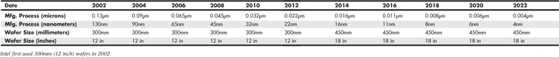
Note that not all the chips on each wafer will be good, especially as a new production line starts. As the manufacturing process for a given chip or production line is perfected, more and more of the chips will be good. The ratio of good to bad chips on a wafer is called the yield. Yields well under 50% are common when a new chip starts production; however, by the end of a given chip’s life, the yields are normally in the 90% range. Most chip manufacturers guard their yield figures and are very secretive about them because knowledge of yield problems can give their competitors an edge. A low yield causes problems both in the cost per chip and in delivery delays to their customers. If a company has specific knowledge of competitors’ improving yields, it can set prices or schedule production to get higher market share at a critical point.
After a wafer is complete, a special fixture tests each of the chips on the wafer and marks the bad ones to be separated out later. The chips are then cut from the wafer using either a high-powered laser or diamond saw.
After being cut from the wafers, the individual dies are then retested, packaged, and retested again. The packaging process is also referred to as bonding because the die is placed into a chip housing in which a special machine bonds fine gold wires between the die and the pins on the chip. The package is the container for the chip die, which essentially seals it from the environment.
After the chips are bonded and packaged, final testing is done to determine both proper function and rated speed. Different chips in the same batch often run at different speeds. Special test fixtures run each chip at different pressures, temperatures, and speeds, looking for the point at which the chip stops working. At this point, the maximum successful speed is noted and the final chips are sorted into bins with those that tested at a similar speed.
One interesting thing about this is that as a manufacturer gains more experience and perfects a particular chip assembly line, the yield of the higher-speed versions goes way up. So, of all the chips produced from a single wafer, perhaps more than 75% of them, check out at the highest speed, and only 25% or less run at the lower speeds. The paradox is that Intel often sells a lot more of the lower-priced, lower-speed chips, so it just dips into the bin of faster ones, labels them as slower chips, and sells them that way. People began discovering that many of the lower-rated chips actually ran at speeds much higher than they were rated, and the business of overclocking was born.
Processor Re-marking
As people learned more about how processors are manufactured and graded, an interesting problem arose: Unscrupulous vendors began re-marking slower chips and reselling them as if they were faster versions. Often the price between the same chip at different speed grades can be substantial—in the hundreds of dollars—so by changing a few numbers on the chip, the potential profits can be huge. Because most of the Intel and AMD processors are produced with a generous safety margin—that is, they typically run well past their rated speeds—the re-marked chips would seem to work fine in most cases. Of course, in many cases they wouldn’t work fine, and the system would end up crashing or locking up periodically.
At first, the re-marked chips were just a case of rubbing off the original numbers and restamping with new official-looking numbers. These were easy to detect, though. Re-markers then resorted to more sophisticated counterfeiting techniques, making remarks harder to detect. This type of re-marking is a form of organized crime and isn’t just some kid in his basement with sandpaper and a rubber stamp.
Intel and AMD have seen fit to put a stop to some of the re-marking by building overclock protection in the form of a multiplier lock into most of their chips since the late ‘90s, except certain models designed for the enthusiast market. This is usually done in manufacturing process, where the chips are intentionally altered so they won’t run at any speeds higher than they are rated. Usually this involves changing the bus frequency (BF) pins or traces on the chip, which control the internal multipliers the chip uses. At one point, many feared that fixing the clock multiplier would put an end to hobbyist overclocking, but that proved not to be the case. Enterprising individuals found ways to run their motherboards at bus speeds higher than normal, so even though the CPU generally won’t allow a higher multiplier, you can still run it at a speed higher than it was designed for by ramping up the speed of the processor bus.
Today’s socketed processors are much more immune to these re-marking attempts, but it is still possible, particularly because the evidence can be hidden under a heatsink. To protect yourself from purchasing a fraudulent chip, verify the specification numbers and serial numbers with Intel and AMD before you purchase. Also beware where you buy your hardware. Online auction sites and traveling computer show/flea market arenas can be a hotbed of this type of activity. Finally, I recommend purchasing only “boxed” or retail-packaged versions of the Intel and AMD processors, rather than the raw OEM versions. The boxed versions are shrink-wrapped and contain a high-quality heatsink, documentation, and a 3-year warranty with the manufacturer.
Fraudulent computer components are not limited to processors. I have seen fake memory, fake mice, fake video cards, fake cache memory, counterfeit operating systems and applications, and even fake motherboards. The hardware that is faked usually works but is of inferior quality to the type it is purporting to be. For example, one of the most highly counterfeited pieces of hardware at one time was the Microsoft mouse. These mice originally sold for $35 wholesale, yet I could purchase cheap mice from overseas manufacturers for as little as $2 each. It didn’t take somebody long to realize that if they made the $2 mouse look like a $35 Microsoft mouse, they could sell it for $20 and people would think they were getting a genuine article for a bargain, while the thieves ran off with a substantial profit.
PGA Chip Packaging
Variations on the pin grid array (PGA) chip packaging have been the most commonly used chip packages over the years. They were used starting with the 286 processor in the 1980s and are still used today, although not in all CPU designs. PGA takes its name from the fact that the chip has a grid-like array of pins on the bottom of the package. PGA chips are inserted into sockets, which are often of a zero insertion force (ZIF) design. A ZIF socket has a lever to allow for easy installation and removal of the chip.
Most Pentium processors use a variation on the regular PGA called staggered pin grid array (SPGA), in which the pins are staggered on the underside of the chip rather than in standard rows and columns. This was done to move the pins closer together and decrease the overall size of the chip when a large number of pins is required. Figure 3.6 shows a Pentium Pro that uses the dual-pattern SPGA (on the right) next to an older Pentium 66 that uses the regular PGA. Note that the right half of the Pentium Pro shown here has additional pins staggered among the other rows and columns.
Figure 3.6 PGA on Pentium 66 (left) and dual-pattern SPGA on Pentium Pro (right).

Older PGA variations had the processor die mounted in a cavity underneath the substrate, with the top surface facing up if you turned the chip upside down. The die was then wire-bonded to the chip package with hundreds of tiny gold wires connecting the connections at the edge of the chip with the internal connections in the package. After the wire bonding, the cavity was sealed with a metal cover. This was an expensive and time-consuming method of producing chips, so cheaper and more efficient packaging methods were designed.
Most modern processors are built on a form of flip-chip pin grid array (FC-PGA) packaging. This type still plugs into a PGA socket, but the package itself is dramatically simplified. With FC-PGA, the raw silicon die is mounted face down on the top of the chip substrate, and instead of wire bonding, the connections are made with tiny solder bumps around the perimeter of the die. The edge is then sealed with a fillet of epoxy. With the original versions of FC-PGA, you could see the backside of the raw die sitting on the chip.
Unfortunately, there were some problems with attaching the heatsink to an FC-PGA chip. The heatsink sat on the top of the die, which acted as a pedestal. If you pressed down on one side of the heatsink excessively during the installation process (such as when you were attaching the clip), you risked cracking the silicon die and destroying the chip. This was especially a problem as heatsinks became larger and heavier and the force applied by the clip became greater.
AMD decreased the risk of damage by adding rubber spacers to each corner of the chip substrate for the Athlon XP, thus preventing the heatsink from tilting excessively during installation. Still, these bumpers could compress, and it was still too easy to crack the die.
Intel revised its packaging with a newer FC-PGA2 version used in later Pentium III and all Pentium 4 processors. This incorporates a protective metal cap, dubbed a heat spreader, to protect the CPU from damage when the heatsink is attached. Ironically, the first processor for PCs to use a heat spreader was actually made by AMD for its K6 family of processors.
All of the Intel processors since the Pentium 4, and AMD processors since the Athlon 64 use a heat spreader on top of the processor die, enabling larger and heavier heatsinks to be installed without any potential damage to the processor core.
Future packaging directions may include what is called bumpless build-up layer (BBUL) packaging. This embeds the die completely in the package; in fact, the package layers are built up around and on top of the die, fully encapsulating it within the package. This embeds the chip die and allows for a full flat surface for attaching the heatsink, as well as shorter internal interconnections within the package. BBUL is designed to handle extremely high clock speeds of 20GHz or faster.
Single Edge Contact and Single Edge Processor Packaging
Intel and AMD used cartridge- or board-based packaging for some of their processors from 1997 through 2000. This packaging was called single edge contact cartridge (SECC) or single edge processor package (SEPP) and consisted of the CPU and optional separate L2 cache chips mounted on a circuit board that looked similar to an oversized memory module and that plugged into a slot. In some cases, the boards were covered with a plastic cartridge cover.
The SEC cartridge is an innovative—if a bit unwieldy—package design that incorporates the back-side bus and L2 cache internally. It was used as a cost-effective method for integrating L2 cache into the processor before it was feasible to include the cache directly inside the processor die.
A less expensive version of the SEC is called the single edge processor (SEP) package. The SEP package is basically the same circuit board containing processor and (optional) cache, but without the fancy plastic cover. This was used mainly by the lower-cost early Celeron processors. The SEP package plugs directly into the same Slot 1 connector used by the standard Pentium II or III. Four holes on the board enable the heatsink to be installed.
Slot 1, as shown in Figure 3.7, is the connection to the motherboard and has 242 pins. AMD used the same physical slot but rotated it 180° and called it Slot A. The SEC cartridge or SEP processor is plugged into the slot and secured with a processor-retention mechanism, which is a bracket that holds it in place. There also might be a retention mechanism or support for the processor heatsink. Figure 3.8 shows the parts of the cover that make up the SEC package. Note the large thermal plate used to aid in dissipating the heat from this processor. The SEP package is shown in Figure 3.9.
Figure 3.7 Pentium II Processor Slot 1 dimensions (metric/English).
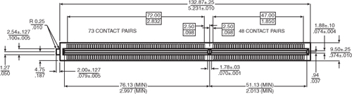
Figure 3.8 Pentium II Processor SEC package parts.

Figure 3.9 Celeron Processor SEP package front-side view.

With the Pentium III, Intel introduced a variation on the SEC packaging called single edge contact cartridge version 2 (SECC2). This new package covered only one side of the processor board with plastic and enables the heatsink to directly attach to the chip on the other side. This more direct thermal interface allowed for better cooling, and the overall lighter package was cheaper to manufacture. A newer Universal Retention System, consisting of a plastic upright stand, was required to hold the SECC2 package chip in place on the board. The Universal Retention System also worked with the older SEC package as used on most Pentium II processors, as well as the SEP package used on the slot-based Celeron processors. This made it the ideal retention mechanism for all Slot 1-based processors. AMD Athlon Slot A processors used the same retention mechanisms as Intel. Figure 3.10 shows the SECC2 package.
Figure 3.10 SECC2 packaging used in Pentium II and III processors.

The main reason for switching to the SEC and SEP packages in the first place was to be able to move the L2 cache memory off the motherboard and onto the processor in an economical and scalable way. This was necessary because, at the time, it was not feasible to incorporate the cache directly into the CPU core die. After building the L2 directly into the CPU die became possible, the cartridge and slot packaging were unnecessary. Because virtually all modern processors incorporate the L2 cache on-die, the processor packaging has gone back to the PGA socket form.
Processor Socket and Slot Types
Intel and AMD have created a set of socket and slot designs for their processors. Each socket or slot is designed to support a different range of original and upgrade processors. Table 3.13 shows the designations for the various standard processor sockets/slots and lists the chips designed to plug into them.
Table 3.13 CPU Socket Specifications
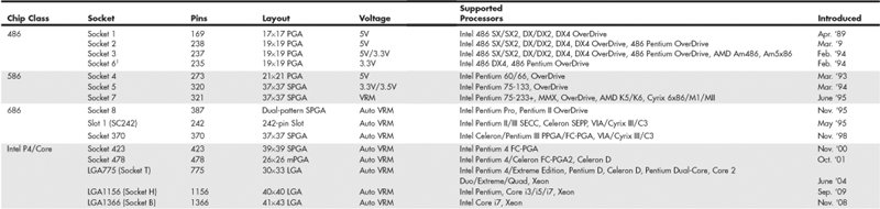

Sockets 1, 2, 3, and 6 are 486 processor sockets and are shown together in Figure 3.11 so you can see the overall size comparisons and pin arrangements between these sockets. Sockets 4, 5, 7, and 8 are Pentium and Pentium Pro processor sockets and are shown together in Figure 3.12 so you can see the overall size comparisons and pin arrangements between these sockets.
Figure 3.11 486 processor sockets.

Figure 3.12 Pentium and Pentium Pro processor sockets.

When the Socket 1 specification was created, manufacturers realized that if users were going to upgrade processors, they had to make the process easier. The socket manufacturers found that 100 lbs. of insertion force is required to install a chip in a standard 169-pin Socket 1 motherboard. With this much force involved, you easily could damage either the chip or the socket during removal or reinstallation. Because of this, some motherboard manufacturers began using low insertion force (LIF) sockets, which required a lesser 60 lbs. of insertion force for a 169-pin chip. Pressing down on the motherboard with 60–100 lbs. of force can crack the board if it is not supported properly. A special tool is also required to remove a chip from one of these sockets. As you can imagine, even the low insertion force was relative, and a better solution was needed if the average person was ever going to replace his CPU.
Manufacturers began using ZIF sockets in Socket 1 designs, and all processor sockets from Socket 2 and higher have been of the ZIF design. ZIF is required for all the higher-density sockets because the insertion force would simply be too great otherwise. ZIF sockets almost eliminate the risk involved in installing or removing a processor because no insertion force is necessary to install the chip and no tool is needed to extract one. Most ZIF sockets are handle-actuated: You lift the handle, drop the chip into the socket, and then close the handle. This design makes installing or removing a processor an easy task.
The following sections take a closer look at those socket designs you are likely to encounter in active PCs.
Socket 370 (PGA-370)
In November 1998, Intel introduced a new socket for P6 class processors. The socket was called Socket 370 or PGA-370 because it has 370 pins and originally was designed for lower-cost PGA versions of the Celeron and Pentium III processors. Socket 370 was originally designed to directly compete in the lower-end system market along with the Super7 platform supported by AMD and Cyrix. However, Intel later used it for the Pentium III processor. Initially all the Celeron and Pentium III processors were made in SECC or SEPP format. These are essentially circuit boards containing the processor and separate L2 cache chips on a small board that plugs into the motherboard via Slot 1. This type of design was necessary when the L2 cache chips were made a part of the processor but were not directly integrated into the processor die. Intel did make a multiple-die chip package for the Pentium Pro, but this proved to be a very expensive way to package the chip, and a board with separate chips was cheaper, which is why the Pentium II looks different from the Pentium Pro.
Starting with the Celeron 300A processor introduced in August 1998, Intel began combining the L2 cache directly on the processor die; it was no longer in separate chips. With the cache fully integrated into the die, there was no longer a need for a board-mounted processor. Because it costs more to make a Slot 1 board or cartridge-type processor instead of a socketed type, Intel moved back to the socket design to reduce the manufacturing cost—especially with the Celeron, which at that time was competing on the low end with Socket 7 chips from AMD and Cyrix.
The Socket 370 (PGA-370) pinout is shown in Figure 3.13.
Figure 3.13 Socket 370 (PGA-370) Pentium III/Celeron pinout (top view).

The Celeron was gradually shifted over to PGA-370, although for a time both were available. All Celeron processors at 333MHz and lower were available only in the Slot 1 version. Celeron processors from 366MHz to 433MHz were available in both Slot 1 and Socket 370 versions; all Celeron processors from 466MHz and up through 1.4GHz are available only in the Socket 370 version.
Starting in October 1999, Intel also introduced Pentium III processors with integrated cache that plug into Socket 370. These use a packaging called flip chip pin grid array (FC-PGA), in which the raw die is mounted on the substrate upside down. The slot version of the Pentium III was more expensive and no longer necessary because of the on-die L2 cache.
Note that because of some voltage changes and one pin change, many original Socket 370 motherboards do not accept the later FC-PGA Socket 370 versions of the Pentium III and Celeron. Pentium III processors in the FC-PGA form have two RESET pins and require VRM 8.4 specifications. Prior motherboards designed only for the older versions of the Celeron are referred to as legacy motherboards, and the newer motherboards supporting the second RESET pin and VRM 8.4 specification are referred to as flexible motherboards. Contact your motherboard or system manufacturer for information to see whether your socket is the flexible version. Some motherboards, such as the Intel CA810, do support the VRM 8.4 specifications and supply proper voltage, but without Vtt support the Pentium III processor in the FC-PGA package will be held in RESET#. The last versions of the Pentium III and Celeron III use the Tualatin core design, which also requires a revised socket to operate. Motherboards that can handle Tualatin-core processors are known as Tualatin-ready and use different chipsets from those not designed to work with the Tualatin-core processor. Companies that sell upgrade processors offer products that enable you to install a Tualatin-core Pentium III or Celeron III processor into a motherboard that lacks built-in Tualatin support.
Installing a Pentium III processor in the FC-PGA package into an older motherboard is unlikely to damage the motherboard. However, the processor itself could be damaged. Pentium III processors in the 0.18-micron process operate at either 1.60V or 1.65V, whereas the Intel Celeron processors operate at 2.00V. The motherboard could be damaged if the motherboard BIOS fails to recognize the voltage identification of the processor. Contact your PC or motherboard manufacturer before installation to ensure compatibility.
A motherboard with a Slot 1 can be designed to accept almost any Celeron, Pentium II, or Pentium III processor. To use the socketed Celerons and Pentium III processors, several manufacturers have made available a low-cost slot-to-socket adapter sometimes called a slot-ket. This is essentially a Slot 1 board containing only a Socket 370, which enables you to use a PGA processor in any Slot 1 board. A typical slot-ket adapter is shown in the “Celeron” section later in this chapter.
![]() See “Celeron,” p. 123 (this chapter).
See “Celeron,” p. 123 (this chapter).
Socket 423
Socket 423 is a ZIF-type socket introduced in November 2000 for the original Pentium 4. Figure 3.14 shows Socket 423.
Figure 3.14 Socket 423 (Pentium 4) showing pin 1 location.

Socket 423 supports a 400MHz processor bus, which connects the processor to the Memory Controller Hub (MCH), which is the main part of the motherboard chipset and similar to the North Bridge in earlier chipsets. Pentium 4 processors up to 2GHz were available for Socket 423; all faster versions require Socket 478 instead.
Socket 423 uses a unique heatsink mounting method that requires standoffs attached either to the chassis or to a special plate that mounts underneath the motherboard. This was designed to support the weight of the larger heatsinks required for the Pentium 4. Because of this, many Socket 423 motherboards require a special chassis that has the necessary additional standoffs installed. Fortunately, the need for these standoffs was eliminated with the newer Socket 478 for Pentium 4 processors.
The processor uses five voltage ID (VID) pins to signal the VRM built into the motherboard to deliver the correct voltage for the particular CPU you install. This makes the voltage selection completely automatic and foolproof. Most Pentium 4 processors for Socket 423 require 1.7V. A small triangular mark indicates the pin-1 corner for proper orientation of the chip.
Socket 478
Socket 478 is a ZIF-type socket for the Pentium 4 and Celeron 4 (Celerons based on the Pentium 4 core) introduced in October 2001. It was specially designed to support additional pins for future Pentium 4 processors and speeds over 2GHz. The heatsink mounting is different from the previous Socket 423, allowing larger heatsinks to be attached to the CPU. Figure 3.15 shows Socket 478.
Figure 3.15 Socket 478 (Pentium 4) showing pin 1 location.
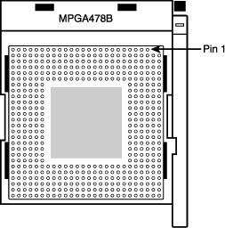
Socket 478 supports a 400MHz, 533MHz, or 800MHz processor bus that connects the processor to the memory controller hub (MCH), which is the main part of the motherboard chipset.
Socket 478 uses a heatsink attachment method that clips the heatsink directly to the motherboard, and not the CPU socket or chassis (as with Socket 423). Therefore, any standard chassis can be used, and the special standoffs used by Socket 423 boards are not required. This heatsink attachment allows for a much greater clamping load between the heatsink and processor, which aids cooling.
Socket 478 processors use five VID pins to signal the VRM built into the motherboard to deliver the correct voltage for the particular CPU you install. This makes the voltage selection completely automatic and foolproof. A small triangular mark indicates the pin-1 corner for proper orientation of the chip.
Socket LGA775
Socket LGA775 (also called Socket T) is used by the Core 2 Duo/Quad processors, the latest versions of the Intel Pentium 4 Prescott processor and the Pentium D and Pentium Extreme Edition processors, as well as some versions of the Celeron and Celeron D. Socket LGA775 is unique in that it uses a land grid array format, so the pins are on the socket, rather than the processor.
LGA uses gold pads (called lands) on the bottom of the processor to replace the pins used in PGA packages. It allows for much greater clamping forces via a load plate with a locking lever, with greater stability and improved thermal transfer (better cooling). The first LGA processors were the Pentium II and Celeron processors in 1997; in those processors LGA chip was soldered on the Slot-1 cartridge. LGA is a recycled version of what was previously called leadless chip carrier (LCC) packaging. This was used way back on the 286 processor in 1984, which had gold lands around the edge only (there were far fewer pins back then). In other ways LGA is simply a modified version of ball grid array (BGA), with gold lands replacing the solder balls, making it more suitable for socketed (rather than soldered) applications. Socket LGA775 is shown in Figure 3.16.
Figure 3.16 Socket LGA775 (Socket T). The release lever on the left is used to raise the load plate out of the way to permit the processor to be placed over the contacts.

Socket LGA1156
Socket LGA1156 (also known as Socket H) was introduced in September 2009, and was designed to support Intel Core i Series processors featuring an integrated chipset north bridge, including a dual-channel DDR3 memory controller and optional integrated graphics. Socket LGA1156 uses a land grid array format, so the pins are on the socket, rather than the processor. Socket LGA1156 is shown in Figure 3.17.
Figure 3.17 Socket LGA1156 (Socket H).
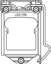
Since the processor includes the chipset north bridge, Socket LGA1156 is designed to interface between a processor and a Platform Controller Hub (PCH), which is the new name used for the south bridge component in supporting 5x series chipsets. The LGA1156 interface includes:
• PCI Express x16 v2.0—For connection to either a single PCIe x16 slot, or two PCIe x8 slots supporting video cards.
• DMI (Direct Media Interface)—For data transfer between the processor and the Platform Controller Hub (PCH). DMI in this case is essentially a modified PCI Express x4 v2.0 connection, with a bandwidth of 2GBps.
• DDR3 dual-channel—For direct connection between the memory controller integrated into the processor and DDR3 SDRAM modules in a dual-channel configuration.
• FDI (Flexible Display Interface)—For the transfer of digital display data between the (optional) processor integrated graphics and the PCH.
When processors with integrated graphics are used, the Flexible Display Interface carries digital display data from the GPU in the processor to the display interface circuitry in the Platform Controller Hub (PCH). Depending on the motherboard, the display interface can support DisplayPort, HDMI, DVI, or VGA connectors.
Socket LGA1366
Socket LGA1366 (also known as Socket B) was introduced in November 2008, and was designed to support high-end Intel Core i Series processors including an integrated triple-channel DDR3 memory controller, but which also requires an external chipset north bridge, in this case called an I/O Hub (IOH). Socket LGA1366 uses a land grid array format, so the pins are on the socket, rather than the processor. Socket LGA1366 is shown in Figure 3.18.
Figure 3.18 Socket LGA1366 (Socket B).

Socket LGA1366 is designed to interface between a processor and an I/O Hub (IOH), which is the new name used for the north bridge component in supporting 5x series chipsets. The LGA1366 interface includes:
• QPI (Quick Path Interconnect)—For data transfer between the processor and the I/O Hub (IOH). QPI transfers 2 bytes per cycle at either 4.8 or 6.4GHz, resulting in a bandwidth of 9.6 or 12.8GBps.
• DDR3 triple-channel—For direct connection between the memory controller integrated into the processor and DDR3 SDRAM modules in a triple-channel configuration.
LGA1366 is designed for high-end PC, workstation, or server use, and supports configurations with multiple processors.
Socket A (Socket 462)
AMD introduced Socket A, also called Socket 462, in June 2000 to support the PGA versions of the Athlon and Duron processors. It is designed as a replacement for Slot A used by the original Athlon processor. Because the Athlon has now moved to incorporate L2 cache on-die, and the low-cost Duron was manufactured only in an on-die cache version, there was no longer a need for the expensive cartridge packaging the original Athlon processors used.
Socket A has 462 pins and 11 plugs oriented in an SPGA form (see Figure 3.19). Socket A has the same physical dimensions and layout as Socket 370; however, the location and placement of the plugs prevent Socket 370 processors from being inserted. Socket A supports 31 voltage levels from 1.100V to 1.850V in 0.025V increments, controlled by the VID0–VID4 pins on the processor. The automatic voltage regulator module circuitry typically is embedded on the motherboard.
Figure 3.19 Socket A (Socket 462) Athlon/Duron layout.
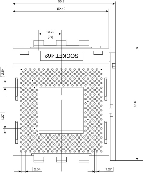
There are 11 total plugged holes, including two of the outside pin holes at A1 and AN1. These are used to allow for keying to force the proper orientation of the processor in the socket.
After the introduction of Socket A, AMD moved all Athlon (including all Athlon XP) processors to this form factor, phasing out Slot A. In addition, for a time AMD also sold a reduced L2 cache version of the Athlon, called the Duron, in this form factor. In 2005, AMD discontinued the Athlon XP and introduced the AMD Sempron in both Socket A and Socket 754 form factors. The first Athlon 64 processors also used Socket 754, but later switched to Socket 939 and AM2.
Caution
Just because a chip can plug into a socket doesn’t mean it will work. The Athlon XP and Socket A Sempron processors require different voltages, BIOS, and chipset support than earlier Socket A Athlon and Duron processors. As always, make sure your motherboard supports the processor you intend to install.
Socket 754
Socket 754 is used with the initial releases of the AMD Athlon 64 processors. Socket 754 is also used by some versions of the AMD Sempron, AMD’s economy processor line. This socket supports single-channel unbuffered DDR SDRAM. Figure 3.20 shows an overhead view of this socket.
Figure 3.20 Socket 754. The large cutout corner at the lower left indicates pin 1.

Socket 939 and 940
Socket 939 is used with the Socket 939 versions of the AMD Athlon 64, 64 FX, and 64 X2 (see Figure 3.21). It’s also used by some recent versions of the AMD Opteron processor for workstations and servers. Motherboards using this socket support conventional unbuffered DDR SDRAM modules in either single- or dual-channel mode, rather than the server-oriented (more expensive) registered modules required by Socket 940 motherboards. Sockets 939 and 940 have different pin arrangements and processors for each and are not interchangeable.
Figure 3.21 Socket 939. The cutout corner and triangle at the lower left indicate pin 1.

Socket 940 is used with the Socket 940 version of the AMD Athlon 64 FX, as well as most AMD Opteron processors (see Figure 3.22). Motherboards using this socket support only registered DDR SDRAM modules in dual-channel mode. Because the pin arrangement is different, Socket 939 processors do not work in Socket 940, and vice versa.
Figure 3.22 Socket 940. The cutout corner and triangle at the lower left indicate pin 1.
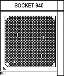
Socket AM2/AM2+/AM3
In May 2006, AMD introduced processors that use a new socket, called Socket AM2 (see Figure 3.23). AM2 was the first replacement for the confusing array of Socket 754, Socket 939, and Socket 940 form factors for the Athlon 64, Athlon 64 FX, and Athlon 64 X2 processors.
Figure 3.23 Socket AM2/AM2+. The arrow (triangle) at the lower left indicates pin 1.

Although Socket AM2 contains 940 pins—the same number as used by Socket 940—Socket AM2 is designed to support the integrated dual-channel DDR2 memory controllers that were added to the Athlon 64 and Opteron processor families in 2006. Processors designed for Sockets 754, 939, and 940 include DDR memory controllers and are not pin compatible with Socket AM2. Sockets 939, 940 and AM2/AM2+ support HyperTransport v2.0, which limits most processors to a 1GHz front-side bus.
Socket AM2+ is an upgrade to Socket AM2 that was released in November 2007. While Sockets AM2 and AM2+ are physically the same, Socket AM2+ adds support for split power planes and HyperTransport 3.0, allowing for front-side bus speeds of up to 2.6GHz. Socket AM2+ chips are backwards compatible with Socket AM2 motherboards, but only at reduced HyperTransport 2.0 front-side bus speeds. Socket AM2 processors can technically work in Socket AM2+ motherboards, however this also requires BIOS support, which is not present in all motherboards.
Socket AM3 was introduced in February 2009, primarily to support processors with integrated DDR3 memory controllers such as the Phenom II. Besides adding support for DDR3 memory, Socket AM3 has 941 pins in a modified key pin configuration that physically prevents Socket AM2 or AM2+ processors from being inserted (see Figure 3.24).
Figure 3.24 Socket AM3. The arrow (triangle) at the lower left indicates pin 1.
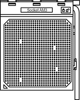
Table 3.14 shows the essential differences between Socket AM2, AM2+ and AM3.
Table 3.14 Socket AM2, AM2+ and AM3 Features

Here is a summary of the compatibility between AM2, AM2+ and AM3 processors and motherboards:
• You cannot install Socket AM2 or AM2+ processors in Socket AM3 motherboards.
• You can install Socket AM2 processors in Socket AM2+ motherboards.
• You can install Socket AM3 or AM2+ processors in Socket AM2 motherboards, however the BIOS must support the processor, the FSB will run at lower HT 2.0 speeds, and only DDR2 memory is supported.
• You can install Socket AM3 processors in Socket AM2+ motherboards, however the BIOS must support the processor, and only DDR2 memory is supported.
While you can physically install newer processors in motherboards with older sockets, and they should theoretically work with reductions in bus speeds and memory support, this also requires BIOS support in the specific motherboard, which may be lacking. In general you are best off matching the processor to a motherboard with the same type of socket.
Socket F (1207FX)
Socket F (also called 1207FX) was initially introduced by AMD in August 2006 for its Opteron line of server processors. Socket F is AMDs first LGA (land grid array) socket (similar to Intel’s Socket LGA775), featuring 1,207 pins in a 35-by-35 grid, with the pins in the socket instead of on the processor. Socket F normally appears on motherboards in pairs because it is designed to run dual physical processors on a single motherboard. Socket F was utilized by AMD for its Quad FX processors, which are dual-core processors sold in matched pairs, operating as a dual socket dual-core system. Future versions may support quad-core processors, for a total of eight cores in the system. Due to the high expense of running dual physical processors, only a very limited number of nonserver motherboards are available with Socket F.
CPU Operating Voltages
One trend that is clear to anybody who has been following processor design is that the operating voltages have gotten lower and lower. The benefits of lower voltage are threefold. The most obvious is that with lower voltage comes lower overall power consumption. By consuming less power, the system is less expensive to run, but more importantly for portable or mobile systems, it runs much longer on existing battery technology. The emphasis on battery operation has driven many of the advances in lowering processor voltage because this has a great effect on battery life.
The second major benefit is that with less voltage and therefore less power consumption, less heat is produced. Processors that run cooler can be packed into systems more tightly and last longer.
The third major benefit is that a processor running cooler on less power can be made to run faster. Lowering the voltage has been one of the key factors in enabling the clock rates of processors to go higher and higher. This is because the lower the voltage, the shorter the time needed to change a signal from low to high.
Starting with the Pentium Pro, all newer processors automatically determine their voltage settings by controlling the motherboard-based voltage regulator. That’s done through built-in VID pins.
For hotrodding purposes, many newer motherboards for these processors have override settings that allow for manual voltage adjustment if desired. Many people have found that when attempting to overclock a processor, increasing the voltage by a tenth of a volt or so often helps. Of course, this increases the heat output of the processor and must be accounted for with adequate heatsinking and case cooling.
Note
Although modern processors use VID pins to enable the processor to select the correct voltage, newer processor that use the same processor socket as older processors might use a voltage setting not supported by the motherboard. Before upgrading an existing motherboard with a new processor, make sure the motherboard will support the processor’s voltage and other features. You might need to install a BIOS upgrade before upgrading the processor to ensure that the processor is properly recognized by the motherboard.
Math Coprocessors (Floating-Point Units)
Older central processing units designed by Intel (and cloned by other companies) used an external math coprocessor chip to perform floating-point operations. However, when Intel introduced the 486DX, it included a built-in math coprocessor, and every processor built by Intel (and AMD and Cyrix, for that matter) since then includes a math coprocessor. Coprocessors provide hardware for floating-point math, which otherwise would create an excessive drain on the main CPU. Math chips speed your computer’s operation only when you are running software designed to take advantage of the coprocessor. All the subsequent fifth- and sixth-generation Intel and compatible processors (such as those from AMD and Cyrix) have featured an integrated floating-point unit.
Math chips (as coprocessors sometimes are called) can perform high-level mathematical operations—long division, trigonometric functions, roots, and logarithms, for example—at 10 to 100 times the speed of the corresponding main processor. The operations performed by the math chip are all operations that make use of noninteger numbers (numbers that contain digits after the decimal point). The need to process numbers in which the decimal is not always the last character leads to the term floating point because the decimal (point) can move (float), depending on the operation. The integer units in the primary CPU work with integer numbers, so they perform addition, subtraction, and multiplication operations. The primary CPU is designed to handle such computations; these operations are not offloaded to the math chip.
The instruction set of the math chip is different from that of the primary CPU. A program must detect the existence of the coprocessor and then execute instructions written explicitly for that coprocessor; otherwise, the math coprocessor draws power and does nothing else. Fortunately, most modern programs that can benefit from the use of the coprocessor correctly detect and use the coprocessor. These programs usually are math intensive: spreadsheet programs, database applications, statistical programs, and graphics programs, such as computer-aided design (CAD) software. Word processing programs do not benefit from a math chip and therefore are not designed to use one. Table 3.15 summarizes the coprocessors available for the Intel family of processors.
Table 3.15 Math Coprocessor Summary
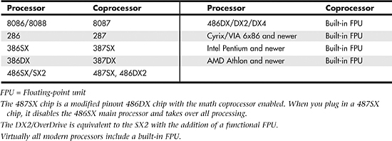
Note
Most applications that formerly used floating-point math now use MMX/SSE instructions instead. These instructions are faster and more accurate than x87 floating-point math.
Processor Bugs and Steppings
Processor manufacturers use specialized equipment to test their own processors, but you have to settle for a little less. The best processor-testing device to which you have access is a system that you know is functional; you then can use the diagnostics available from various utility software companies or your system manufacturer to test the motherboard and processor functions.
Perhaps the most infamous of these bugs is the floating-point division math bug in the early Pentium processors. This and a few other bugs are discussed in detail later in this chapter.
Because the processor is the brain of a system, most systems don’t function with a defective processor. If a system seems to have a dead motherboard, try replacing the processor with one from a functioning motherboard that uses the same CPU chip. You might find that the processor in the original board is the culprit. If the system continues to play dead, however, the problem is elsewhere, most likely in the motherboard, memory, or power supply. See the chapters that cover those parts of the system for more information on troubleshooting those components. I must say that in all my years of troubleshooting and repairing PCs, I have rarely encountered defective processors.
A few system problems are built in at the factory, although these bugs or design defects are rare. By learning to recognize these problems, you can avoid unnecessary repairs or replacements. Each processor section describes several known defects in that generation of processors, such as the infamous floating-point error in the Pentium. For more information on these bugs and defects, see the following sections, and check with the processor manufacturer for updates.
Processor Code Names
Intel, AMD, and Cyrix have always used code names when talking about future processors as well as processor cores. The code names usually are not supposed to become public, but they often do. They can often be found in online and print news and magazine articles talking about future-generation processors. Sometimes they even appear in motherboard manuals because the manuals are written before the processors are officially introduced.
Intel publishes a fairly complete list of processor, chipset, motherboard, and even Ethernet controller code names on its website (http://ark.intel.com/#codenames). AMD doesn’t publish code names on its own site; however, you can usually find such information on other sites by doing a search.
P1 (086) Processors
Intel introduced the 8086 back in June 1978. The 8086 was one of the first 16-bit processor chips on the market; at the time, virtually all other processors were 8-bit designs. The 8086 had 16-bit internal registers and could run a new class of software using 16-bit instructions. It also had a 16-bit external data path, so it could transfer data to memory 16 bits at a time.
The address bus was 20 bits wide, which enabled the 8086 to address a full 1MB (220) of memory. This was in stark contrast to most other chips of that time that had 8-bit internal registers, an 8-bit external data bus, and a 16-bit address bus allowing a maximum of only 64KB of RAM (216).
Unfortunately, most of the personal computer world at the time was using 8-bit processors, which ran 8-bit CP/M (Control Program for Microprocessors) operating systems and software. The board and circuit designs at the time were largely 8-bit, as well. Building a full 16-bit motherboard and memory system was costly, pricing such a computer out of the market.
The cost was high because the 8086 needed a 16-bit data bus rather than a less expensive 8-bit bus. Systems available at that time were 8-bit, and slow sales of the 8086 indicated to Intel that people weren’t willing to pay for the extra performance of the full 16-bit design. In response, Intel introduced a kind of crippled version of the 8086, called the 8088. The 8088 essentially deleted 8 of the 16 bits on the data bus, making the 8088 an 8-bit chip as far as data input and output were concerned. However, because it retained the full 16-bit internal registers and the 20-bit address bus, the 8088 ran 16-bit software and was capable of addressing a full 1MB of RAM.
For these reasons, IBM selected the 8-bit 8088 chip for the original IBM PC. Years later, IBM was criticized for using the 8-bit 8088 instead of the 16-bit 8086. In retrospect, it was a very wise decision. IBM even covered up the physical design in its ads, which at the time indicated its new PC had a “high-speed 16-bit microprocessor.” IBM could say that because the 8088 still ran the same powerful 16-bit software the 8086 ran, just a little more slowly. In fact, programmers universally thought of the 8088 as a 16-bit chip because there was virtually no way a program could distinguish an 8088 from an 8086. This enabled IBM to deliver a PC capable of running a new generation of 16-bit software, while retaining a much less expensive 8-bit design for the hardware. Because of this, the IBM PC was actually priced less at its introduction than the most popular PC of the time, the Apple II. For the trivia buffs out there, the IBM PC listed for $1,265 and included only 16KB of RAM, whereas a similarly configured Apple II cost $1,355.
Even though the 8088 was introduced in June 1979, the original IBM PC that used the processor did not appear until August 1981. Back then, a significant lag time often occurred between the introduction of a new processor and systems that incorporated it. That is unlike today, when new processors and systems using them often are released on the same day.
The 8088 in the IBM PC ran at 4.77MHz; the average instruction on the 8088 took 12 cycles to complete.
Computer users sometimes wonder why a 640KB conventional-memory barrier exists if the 8088 chip can address 1MB of memory. The conventional-memory barrier exists because IBM reserved 384KB of the upper portion of the 1,024KB (1MB) address space of the 8088 for use by adapter cards and system BIOS. The lower 640KB is the conventional memory in which DOS and software applications execute.
P2 (286) Processors
The Intel 80286 (normally abbreviated as 286) processor, which Intel introduced in 1982 and was the first CPU behind the original IBM PC AT (Advanced Technology), did not suffer from the compatibility problems that damned the 80186 and 80188. Other computer makers manufactured what came to be known as IBM clones, with many of these manufacturers calling their systems AT-compatible or AT-class computers.
When IBM developed the AT, it selected the 286 as the basis for the new system because the chip provided compatibility with the 8088 used in the PC and the XT. Therefore, software written for those chips should run on the 286. The 286 chip is many times faster than the 8088 used in the XT, and at the time it offered a major performance boost to PCs used in businesses. The processing speed, or throughput, of the original AT (which ran at 6MHz) is five times greater than that of the PC running at 4.77MHz. The die for the 286 is shown in Figure 3.25.
Figure 3.25 286 Processor die. Photograph used by permission of Intel Corporation.
Intel 286 systems are faster than their predecessors for several reasons. The main reason is that 286 processors are much more efficient in executing instructions. An average instruction takes 12 clock cycles on the 8086 or 8088, but takes an average of only 4.5 cycles on the 286 processor. Additionally, instead of moving 8 bits of data at a time, the 286 chip can handle up to 16 bits of data at a time through an external data bus twice the size of the 8088.
The 286 chip has two modes of operation: real mode and protected mode. The two modes are distinct enough to make the 286 resemble two chips in one. In real mode, a 286 acts essentially the same as an 8086 chip and is fully object-code compatible with the 8086 and 8088. (A processor with object-code compatibility can run programs written for another processor without modification and execute every system instruction in the same manner.)
In the protected mode of operation, the 286 was truly something new. In this mode, a program designed to take advantage of the chip’s capabilities believes that it has access to 1GB of memory (including virtual memory). The 286 chip, however, can address only 16MB of hardware memory. A significant failing of the 286 chip is that it cannot switch from protected mode to real mode without a hardware reset (a warm reboot) of the system. (It can, however, switch from real mode to protected mode without a reset.) A major improvement of the 386 over the 286 is that software can switch the 386 from real mode to protected mode, and vice versa. See the section “Processor Modes,” earlier in this chapter for more information.
Only a small amount of software that took advantage of the 286 chip was sold until Windows 3.0 offered standard mode for 286 compatibility; by that time, the hottest-selling chip was the 386. Still, the 286 was Intel’s first attempt to produce a CPU chip that supported multitasking, in which multiple programs run at the same time.
P3 (386) Processors
The third generation represents perhaps the most significant change in processors since the first PC. The big deal was the migration from processors that handled 16-bit operations to true 32-bit chips. The third-generation processors were so far ahead of their time that it took fully 10 years before 32-bit operating systems and software became mainstream, and by that time the third-generation chips had become a memory.
The Intel 80386 (usually abbreviated as 386) caused quite a stir in the PC industry because of the vastly improved performance it brought to the personal computer. Compared with 8088 and 286 systems, the 386 chip offered greater performance in almost all areas of operation.
The 386 is a full 32-bit processor optimized for high-speed operation and multitasking operating systems. Intel introduced the chip in 1985, but the 386 appeared in the first systems in late 1986 and early 1987. The Compaq Deskpro 386 and systems made by several other manufacturers introduced the chip; somewhat later, IBM used the chip in its PS/2 Model 80.
The 386 can execute the real-mode instructions of an 8086 or 8088, but in fewer clock cycles. The 386 was as efficient as the 286 in executing instructions—the average instruction took about 4.5 clock cycles. In raw performance, therefore, the 286 and 386 actually seemed to be at almost equal clock rates. The 386 offered greater performance in other ways, mainly because of additional software capability (modes) and a greatly enhanced memory management unit (MMU). The die for the 386 is shown in Figure 3.26.
Figure 3.26 386 processor die. Photograph used by permission of Intel Corporation.

The 386 can switch to and from protected mode under software control without a system reset—a capability that makes using protected mode more practical. In addition, the 386 includes a new mode, called virtual real mode, which enables several real mode sessions to run simultaneously under protected mode.
The protected mode of the 386 is fully compatible with the protected mode of the 286. Intel extended the memory-addressing capabilities of 386 protected mode with a new MMU that provided advanced memory paging and program switching. These features were extensions of the 286 type of MMU, so the 386 remained fully compatible with the 286 at the system-code level.
The 386 chip’s virtual real mode was also new. In virtual real mode, the processor could run with hardware memory protection while simulating an 8086’s real mode operation. Multiple copies of DOS and other operating systems, therefore, could run simultaneously on this processor, each in a protected area of memory. If the programs in one segment crashed, the rest of the system was protected.
Numerous variations of the 386 chip were manufactured, some of which are less powerful and some of which are less power hungry. The following sections cover the members of the 386-chip family and their differences.
386DX Processors
The 386DX chip was the first of the 386 family members that Intel introduced. The 386 is a full 32-bit processor with 32-bit internal registers, a 32-bit internal data bus, and a 32-bit external data bus. The 386 contains 275,000 transistors in a very large scale integration (VLSI) circuit. The chip comes in a 132-pin package and draws approximately 400 milliamperes (ma), which is less power than even the 8086 requires. The 386 has a smaller power requirement because it is made of Complementary Metal-Oxide Semiconductor (CMOS) materials. The CMOS design enables devices to consume extremely low levels of power.
The Intel 386 chip was available in clock speeds ranging from 16MHz–33MHz; other manufacturers, primarily AMD and Cyrix, offered comparable versions with speeds up to 40MHz.
The 386DX can address 4GB of physical memory. Its built-in virtual memory manager enables software designed to take advantage of enormous amounts of memory to act as though a system has 64TB of memory. (A terabyte, or TB, is 1,099,511,627,776 bytes of memory, or about 1,000GB.)
386SX Processors
The 386SX was designed for systems designers looking for 386 capabilities at 286 system prices. Similar to the 286, the 386SX is restricted to only 16 bits when communicating with other system components, such as memory. Internally, however, the 386SX is identical to the DX chip; the 386SX has 32-bit internal registers and can therefore run 32-bit software. The 386SX uses a 24-bit memory-addressing scheme like that of the 286, rather than the full 32-bit memory address bus of the standard 386. The 386SX, therefore, can address a maximum 16MB of physical memory rather than the 4GB of physical memory the 386DX can address. Before it was discontinued, the 386SX was available in clock speeds ranging from 16MHz to 33MHz.
The 386SX signaled the end of the 286 because of the 386SX chip’s superior MMU and the addition of the virtual real mode. Under a software manager such as Windows or OS/2, the 386SX can run numerous DOS programs at the same time. The capability to run 386-specific software is another important advantage of the 386SX over any 286 or older design. For example, Windows 3.1 runs nearly as well on a 386SX as it does on a 386DX.
386SL Processors
The 386SL is another variation on the 386 chip. This low-power CPU had the same capabilities as the 386SX, but it was designed for laptop systems in which low power consumption was necessary. The SL chips offered special power-management features that were important to systems that ran on batteries. The SL chip also offered several sleep modes to conserve power.
The chip included an extended architecture that contained a System Management Interrupt (SMI), which provided access to the power-management features. Also included in the SL chip was special support for LIM (Lotus Intel Microsoft) expanded memory functions and a cache controller. The cache controller was designed to control a 16KB–64KB external processor cache.
These extra functions account for the higher transistor count in the SL chips (855,000) compared with even the 386DX processor (275,000). The 386SL was available in 25MHz clock speed.
P4 (486) Processors
Although fourth generation processors were more about refinement than redesign, the Intel 80486 (normally abbreviated as 486) was another major leap forward in the race for speed. The additional power available in the 486 fueled tremendous growth in the software industry. Tens of millions of copies of Windows, and millions of copies of OS/2, have been sold largely because the 486 finally made the GUI of Windows and OS/2 a realistic option for people who work on their computers every day.
The 486 is a family of processors, consisting of DX, SX, and a number of other variations. Four main features make 486 processors roughly twice as fast as an equivalent MHz 386 chip:
• Reduced instruction-execution time—A single instruction in the 486 takes an average of only two clock cycles to complete, compared with an average of more than four cycles on the 386.
• Internal (Level 1) cache—The built-in cache has a hit ratio of 90%–95%, which describes how often zero-wait-state read operations occur. External caches can improve this ratio further.
• Burst-mode memory cycles—A standard 32-bit (4-byte) memory transfer takes two clock cycles. After a standard 32-bit transfer, more data up to the next 12 bytes (or three transfers) can be transferred with only one cycle used for each 32-bit (4-byte) transfer. Thus, up to 16 bytes of contiguous, sequential memory data can be transferred in as little as five cycles instead of eight cycles or more. This effect can be even greater when the transfers are only 8 bits or 16 bits each.
• Built-in (synchronous) enhanced math coprocessor (some versions)—The math coprocessor runs synchronously with the main processor and executes math instructions in fewer cycles than previous designs did. On average, the math coprocessor built into the DX-series chips provides two to three times greater math performance than an external 387 math coprocessor chip.
The 486 chip is about twice as fast as the 386 at the same clock rate. You can see why the arrival of the 486 rapidly killed off the 386 in the marketplace.
486DX Processors
The original Intel 486DX processor was introduced on April 10, 1989, and systems using this chip first appeared during 1990. The first chips had a maximum speed rating of 25MHz; later versions of the 486DX were available in 33MHz- and 50MHz-rated versions. The 486DX originally was available only in a 5V, 168-pin PGA version, but later became available in 5V, 196-pin plastic quad flat pack (PQFP) and 3.3V, 208-pin small quad flat pack (SQFP). These latter form factors were available in SL enhanced versions, which were intended primarily for portable or laptop applications in which saving power is important.
The 486DX processor was fabricated with low-power CMOS technology. The chip has a 32-bit internal register size, a 32-bit external data bus, and a 32-bit address bus. These dimensions are equal to those of the 386DX processor. The internal register size is where the “32-bit” designation used in advertisements comes from. The 486DX chip contains 1.2 million transistors on a piece of silicon no larger than your thumbnail. This figure is more than four times the number of components on 386 processors and should give you a good indication of the 486 chip’s relative power. The die for the 486 is shown in Figure 3.27.
Figure 3.27 486 processor die. Photograph used by permission of Intel Corporation.

The standard 486DX contains a processing unit, floating-point unit (math coprocessor), memory-management unit, and cache controller with 8KB of internal-cache RAM. Due to the internal cache and a more efficient internal processing unit, the 486 family of processors can execute individual instructions in an average of only two processor cycles. Compare this figure with the 286 and 386 families, both of which execute an average 4.5 cycles per instruction. Compare it also with the original 8086 and 8088 processors, which execute an average 12 cycles per instruction. At a given clock rate (MHz), therefore, a 486 processor is roughly twice as efficient as a 386 processor.
486SL
The 486SL was a short-lived, standalone chip. The SL enhancements and features became available in virtually all the 486 processors (SX, DX, and DX2) in what are called SL enhanced versions. SL enhancement refers to a special design that incorporates special power-saving features.
The SL enhanced chips originally were designed to be installed in laptop or notebook systems that run on batteries, but they found their way into desktop systems as well. The SL-enhanced chips featured special power-management techniques, such as sleep mode and clock throttling, to reduce power consumption when necessary. These chips were available in 3.3V versions as well.
Intel designed a power-management architecture called System Management Mode (SMM). This mode of operation is totally isolated and independent from other CPU hardware and software. SMM provides hardware resources such as timers, registers, and other I/O logic that can control and power down mobile-computer components without interfering with any of the other system resources. SMM executes in a dedicated memory space called System Management Memory, which is not visible and does not interfere with operating system and application software. SMM has an interrupt called System Management Interrupt (SMI), which services power-management events and is independent from—and a higher priority than—any of the other interrupts.
SMM provides power management with flexibility and security that were not available previously. For example, an SMI occurs when an application program tries to access a peripheral device that is powered down for battery savings, which powers up the peripheral device and re-executes the I/O instruction automatically.
Intel also designed a feature called Suspend/Resume in the SL processor. The system manufacturer can use this feature to provide the portable computer user with instant on-and-off capability. An SL system typically can resume (instant on) in 1 second from the suspend state (instant off) to exactly where it left off. You do not need to reboot, load the operating system, or load the applications and their data. Instead, simply push the Suspend/Resume button and the system is ready to go.
The SL CPU was designed to consume almost no power in the suspend state. This feature means that the system can stay in the suspend state possibly for weeks and yet start up instantly right where it left off. An SL system can keep working data in normal RAM memory safe for a long time while it is in the suspend state, but saving to a disk still is prudent.
DX2/OverDrive and DX4 Processors
On March 3, 1992, Intel introduced the DX2 speed-doubling processors. On May 26, 1992, Intel announced that the DX2 processors also would be available in a retail version called OverDrive. Originally, the OverDrive versions of the DX2 were available only in 169-pin versions, which meant that they could be used only with 486SX systems that had sockets configured to support the rearranged pin configuration.
On September 14, 1992, Intel introduced 168-pin OverDrive versions for upgrading 486DX systems. These processors could be added to existing 486 (SX or DX) systems as an upgrade, even if those systems did not support the 169-pin configuration. When you use this processor as an upgrade, you install the new chip in your system, which subsequently runs twice as fast.
The DX2/OverDrive processors run internally at twice the clock rate of the host system. If the motherboard clock is 25MHz, for example, the DX2/OverDrive chip runs internally at 50MHz; likewise, if the motherboard is a 33MHz design, the DX2/OverDrive runs at 66MHz. The DX2/OverDrive speed doubling has no effect on the rest of the system; all components on the motherboard run the same as they do with a standard 486 processor. Therefore, you do not have to change other components (such as memory) to accommodate the double-speed chip.
AMD 486 (5x86)
AMD made a line of 486-compatible chips that installed into standard 486 motherboards. In fact, AMD made the fastest 486 processor available, which it called the Am5x86-P75. The name was a little misleading because the 5x86 part made some people think that this was a fifth-generation Pentium-type processor. In reality, it was a fast clock-multiplied (4x clock) 486 that ran at four times the speed of the 33MHz 486 motherboard you plugged it into.
The 5x86 offered high-performance features such as a unified 16KB write-back cache and 133MHz core clock speed; it was approximately comparable to a Pentium 75, which is why it was denoted with a P75 in the part number. It was the ideal choice for cost-effective 486 upgrades, where changing the motherboard is difficult or impossible.
P5 (586) Processors
After the fourth-generation chips such as the 486, Intel and other chip manufacturers went back to the drawing board to come up with new architectures and features that they would later incorporate into what they called fifth-generation chips.
On October 19, 1992, Intel announced that the fifth generation of its compatible microprocessor line (code-named P5) would be named the Pentium processor rather than the 586, as everybody had assumed. Calling the new chip the 586 would have been natural, but Intel discovered that it could not trademark a number designation, and the company wanted to prevent other manufacturers from using the same name for any clone chips it might develop. The actual Pentium chip shipped on March 22, 1993. Systems that used these chips were only a few months behind.
The Pentium is fully compatible with previous Intel processors, but it differs from them in many ways. At least one of these differences is revolutionary: The Pentium features twin data pipelines, which enable it to execute two instructions at the same time. The 486 and all preceding chips can perform only a single instruction at a time. Intel calls the capability to execute two instructions at the same time superscalar technology. This technology provides additional performance compared with the 486.
With superscalar technology, the Pentium can execute many instructions at a rate of two instructions per cycle. Superscalar architecture usually is associated with high-output RISC chips. The Pentium is one of the first CISC chips to be considered superscalar. The Pentium is almost like having two 486 chips under the hood. Table 3.16 shows the Pentium processor specifications.
Table 3.16 Pentium Processor Specifications

The two instruction pipelines within the chip are called the u- and v-pipes. The u-pipe, which is the primary pipe, can execute all integer and floating-point instructions. The v-pipe is a secondary pipe that can execute only simple integer instructions and certain floating-point instructions. The process of operating on two instructions simultaneously in the different pipes is called pairing. Not all sequentially executing instructions can be paired, and when pairing is not possible, only the u-pipe is used. To optimize the Pentium’s efficiency, you can recompile software to enable more instructions to be paired.
The Pentium processor has a branch target buffer (BTB), which employs a technique called branch prediction. It minimizes stalls in one or more of the pipes caused by delays in fetching instructions that branch to nonlinear memory locations. The BTB attempts to predict whether a program branch will be taken and then fetches the appropriate instructions. The use of branch prediction enables the Pentium to keep both pipelines operating at full speed. Figure 3.28 shows the internal architecture of the Pentium processor.
Figure 3.28 Pentium processor internal architecture.
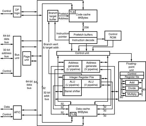
The Pentium has a 32-bit address bus width, giving it the same 4GB memory-addressing capabilities as the 386DX and 486 processors. But the Pentium expands the data bus to 64 bits, which means it can move twice as much data into or out of the CPU, compared with a 486 of the same clock speed. The 64-bit data bus requires that system memory be accessed 64 bits wide, so each bank of memory is 64 bits.
Even though the Pentium has a 64-bit data bus that transfers information 64 bits at a time into and out of the processor, the Pentium has only 32-bit internal registers. As instructions are being processed internally, they are broken down into 32-bit instructions and data elements and processed in much the same way as in the 486. Some people thought that Intel was misleading them by calling the Pentium a 64-bit processor, but 64-bit transfers do indeed take place. Internally, however, the Pentium has 32-bit registers that are fully compatible with the 486.
The Pentium, like the 486, contains an internal math coprocessor or FPU. The FPU in the Pentium was rewritten to perform significantly better than the FPU in the 486 yet still be fully compatible with the 486 and 387 math coprocessors. The Pentium FPU is estimated to be two to as much as ten times faster than the FPU in the 486. In addition, the two standard instruction pipelines in the Pentium provide two units to handle standard integer math. (The math coprocessor handles only more complex calculations.) Other processors, such as the 486, have only a single standard execution pipe and one integer math unit. Interestingly, the Pentium FPU contains a flaw that received widespread publicity. See the discussion in the section “Pentium Defects,” later in this chapter.
First-Generation Pentium Processors
The Pentium was offered in three basic designs, each with several versions. The first-generation design came in 60MHz and 66MHz processor speeds. This design used a 273-pin PGA form factor and ran on 5V power. In this design, the processor ran at the same speed as the motherboard—in other words, a 1x clock was used.
The first-generation Pentium was created through a 0.8-micron BiCMOS process. Unfortunately, this process, combined with the 3.1 million transistor count, resulted in a die that was overly large and complicated to manufacture. As a result, reduced yields kept the chip in short supply; Intel could not make them fast enough. The 0.8-micron process was criticized by other manufacturers, including Motorola and IBM, which had been using 0.6-micron technology for their most advanced chips. The huge die and 5V operating voltage caused the 66MHz versions to consume up to an incredible 3.2 amps or 16 watts of power, resulting in a tremendous amount of heat and problems in some systems that did not employ conservative design techniques. Fortunately, adding a fan to the processor solved most cooling problems, as long as the fan kept running.
Second-Generation Pentium Processors
Intel announced the second-generation Pentium on March 7, 1994. This processor was introduced in 90MHz and 100MHz versions, with a 75MHz version not far behind. Eventually, 120MHz, 133MHz, 150MHz, 166MHz, and 200MHz versions were also introduced. The second-generation Pentium uses 0.6-micron (75/90/100MHz) BiCMOS technology to shrink the die and reduce power consumption. The newer, faster 120MHz (and higher) second-generation versions incorporate an even smaller die built on a 0.35-micron BiCMOS process. These smaller dies are not changed from the 0.6-micron versions; they are basically a photographic reduction of the P54C die. The die for the Pentium is shown in Figure 3.29. Additionally, these processors run on 3.3V power. The 100MHz version consumes a maximum of 3.25 amps of 3.3V power, which equals only 10.725 watts. Further up the scale, the 150MHz chip uses 3.5 amps of 3.3V power (11.6 watts), the 166MHz unit draws 4.4 amps (14.5 watts), and the 200MHz processor uses 4.7 amps (15.5 watts).
Figure 3.29 Pentium processor die. Photograph used by permission of Intel Corporation.

The second-generation Pentium processors use a 296-pin SPGA form factor that is physically incompatible with the first-generation versions. The only way to upgrade from the first generation to the second was to replace the motherboard. The second-generation Pentium processors also have 3.3 million transistors—more than the earlier chips. The extra transistors exist because additional clock-control SL enhancements were added, along with an on-chip advanced programmable interrupt controller (APIC) and dual-processor interface.
The APIC and dual-processor interfaces are responsible for orchestrating dual-processor configurations in which two second-generation Pentium chips can process on the same motherboard simultaneously. Many of the Pentium motherboards designed for file servers come with dual Socket 7 specification sockets, which fully support the multiprocessing capability of the new chips. Software support for what usually is called symmetric multiprocessing (SMP) was integrated into operating systems such as Windows NT and OS/2.
The second-generation Pentium processors use clock-multiplier circuitry to run the processor at speeds faster than the bus. The 150MHz Pentium processor, for example, can run at 2.5 times the bus frequency, which normally is 60MHz. The 200MHz Pentium processor can run at a 3x clock in a system using a 66MHz bus speed.
Virtually all Pentium motherboards had three speed settings: 50MHz, 60MHz, and 66MHz. Pentium chips were available with a variety of internal clock multipliers that caused the processor to operate at various multiples of these motherboard speeds. Refer to Table 3.17 for a list of the speeds of Pentium processors and motherboard bus speeds.
Table 3.17 Pentium BFx Pins and Clock Multipliers

The core-to-bus frequency ratio or clock multiplier is controlled in a Pentium processor by two pins on the chip labeled BF1 and BF2. Table 3.20 shows how the state of the BFx pins affects the clock multiplication in the Pentium processor.
Not all chips support all the bus frequency (BF) pins or combinations of settings. In other words, some of the Pentium processors operate only at specific combinations of these settings or might even be fixed at one particular setting. Many of the later Pentium motherboards included jumpers or switches that enabled you to control the BF pins and, therefore, alter the clock-multiplier ratio within the chip. In theory, you could run a 75MHz-rated Pentium chip at 133MHz by changing jumpers on the motherboard. This is called overclocking and is discussed in the section “Overclocking” in this chapter.
Pentium-MMX Processors
A third generation of Pentium processors (code-named P55C) was released in January 1997, and incorporates what Intel calls MMX technology into the second-generation Pentium design (see Figure 3.30). These Pentium-MMX processors were manufactured in clock rates of 66/166MHz, 66/200MHz, and 66/233MHz and in a mobile-only version, which is 66/266MHz. The MMX processors have a lot in common with other second-generation Pentiums, including superscalar architecture, multiprocessor support, on-chip local APIC controller, and power-management features. New features include a pipelined MMX unit, 16KB code, write-back cache (versus 8KB in earlier Pentiums), and 4.5 million transistors. Pentium-MMX chips are produced on an enhanced 0.35-micron CMOS silicon process that allows for a lower 2.8V voltage level. The newer mobile 233MHz and 266MHz processors are built on a 0.25-micron process and run on only 1.8V. With this newer technology, the 266 processor actually uses less power than the non-MMX 133.
Figure 3.30 Pentium MMX. The left side shows the underside of the chip with the cover plate removed exposing the processor die. Photograph used by permission of Intel Corporation.
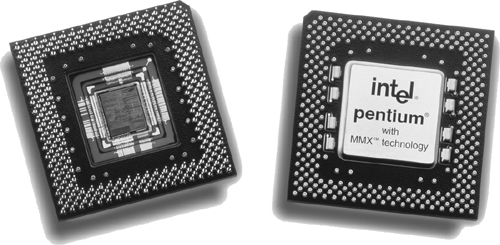
To use the Pentium-MMX, the motherboard must be capable of supplying the lower (2.8V or less) voltage these processors use. To enable a more universal motherboard solution with respect to these changing voltages, Intel developed the Socket 7 with VRM. The VRM is a socketed module that plugs in next to the processor and supplies the correct voltage. Because the module is easily replaced, reconfiguring a motherboard to support any of the voltages required by the newer Pentium processors is easy.
Of course, lower voltage is nice, but MMX is what this chip is really all about. MMX incorporates a process Intel calls single instruction multiple data (SIMD), which enables one instruction to perform the same function on many pieces of data. Fifty-seven new instructions designed specifically to handle video, audio, and graphics data have been added to the chip.
Pentium Defects
Probably the most famous processor bug in history is the now legendary flaw in the Pentium FPU. It has often been called the FDIV bug because it affects primarily the FDIV (floating-point divide) instruction, although several other instructions that use division are also affected. Intel officially refers to this problem as Errata No. 23, titled “Slight precision loss for floating-point divides on specific operand pairs.” The bug has been fixed in the D1 and later steppings of the 60/66MHz Pentium processors, as well as the B5 and later steppings of the 75/90/100MHz processors. The 120MHz and higher processors are manufactured from later steppings, which do not include this problem.
This bug caused a tremendous fervor when it first was reported on the Internet by mathematician Thomas R. Nicely of Lynchburg College in Virginia in October 1994. Within a few days, news of the defect had spread nationwide, and even people who did not have computers had heard about it. The Pentium incorrectly performed floating-point division calculations with certain number combinations, with errors anywhere from the third digit on up. Here is an example of one of the more severe instances of the problem:
962,306,957,033 / 11,010,046 = 87,402.6282027341 (correct answer)
962,306,957,033 / 11,010,046 = 87,399.5805831329 (flawed Pentium)
By the time the bug was publicly discovered outside of Intel, the company had already incorporated the fix into the next stepping of both the 60/66MHz and the 75/90/100MHz Pentium processor, along with the other corrections Intel had made.
After the bug was made public and Intel admitted to already knowing about it, a fury erupted. As people began checking their spreadsheets and other math calculations, many discovered they had also encountered this problem and did not know it. Others who had not encountered the problem had their faith in the core of their PCs shaken. People had come to put so much trust in the PC that they had a hard time coming to terms with the fact that it might not even be capable of doing math correctly!
One interesting result of the fervor surrounding this defect that continues to this day is that people are less inclined to implicitly trust their PCs and are therefore doing more testing and evaluating of important results. The bottom line is that if your information and calculations are important enough, you should implement some results tests. Several math programs were found to have problems. For example, a bug was discovered in the yield function of Excel 5.0 that some were attributing to the Pentium processor. In this case, the problem turned out to be the software (which has been corrected in versions 5.0c and later).
Intel finally decided that in the best interest of the consumer and its public image, it would begin a lifetime replacement warranty on the affected processors. Therefore, if you ever encounter one of the Pentium processors with the Errata 23 floating-point bug, Intel will replace the processor with an equivalent one without this problem.
If you are still using a Pentium-based system and wonder whether you might have a system affected by this bug, visit the Intel “FDIV Replacement Program” page at http://support.intel.com/support/processors/pentium/fdiv/. Here you can find information on how to determine whether your processor is affected and how to obtain a free replacement for an affected processor.
AMD-K5
The AMD-K5 is a Pentium-compatible processor developed by AMD and available as the PR75, PR90, PR100, PR120, PR133, PR166, and PR200. Because it is designed to be physically and functionally compatible, any motherboard that properly supports the Intel Pentium should support the AMD-K5. However, a BIOS upgrade might be required to properly recognize the AMD-K5. The K5 has the following features:
• 16KB instruction cache, 8KB write-back data cache
• Dynamic execution-branch prediction with speculative execution
• Five-stage, RISC-like pipeline with six parallel functional units
• High-performance floating-point unit
• Pin-selectable clock multiples of 1.5x, 1.75x, and 2x
The K5 is sold under the P-Rating system, which means that the number on the chip does not indicate true clock speed, only apparent speed when running certain applications.
Note that the actual clock speeds of several of these processors are not the same as their apparent rated speeds. For example, the PR-166 version actually runs at only 117 true MHz. Sometimes this can confuse the system BIOS, which might report the true speed rather than the P-Rating, which compares the chip against an Intel Pentium of that speed. AMD’s assertion is that because of architecture enhancements over the Pentium, they do not need to run the same clock frequency to achieve that same performance. Even with such improvements, AMD marketed the K5 as a fifth-generation processor, just like the Pentium.
The AMD-K5 operates at 3.52V (VRE setting). Some older motherboards default to 3.3V, which is below specification for the K5 and could cause erratic operation. Because of the relatively low clock speeds and compatibility issues some users experienced with the K5, AMD replaced it with the K6 family of processors.
Intel P6 (686) Processors
The P6 (686) processors represent a new generation with features not found in the previous generation units. The P6 processor family began when the Pentium Pro was released in November 1995. Since then, Intel has released many other P6 chips, all using the same basic P6 core processor as the Pentium Pro. Table 3.18 shows the variations in the P6 family of processors.
Table 3.18 Intel P6 Processor Variations

The main new feature in the fifth-generation Pentium processors was the superscalar architecture, in which two instruction execution units could execute instructions simultaneously in parallel. Later fifth-generation chips also added MMX technology to the mix. So then what did Intel add in the sixth generation to justify calling it a whole new generation of chip? Besides many minor improvements, the real key features of all sixth-generation processors are Dynamic Execution and the Dual Independent Bus (DIB) architecture, plus a greatly improved superscalar design.
Pentium Pro Processors
Intel’s successor to the Pentium is called the Pentium Pro. The Pentium Pro was the first chip in the P6 or sixth-generation processor family. It was introduced in November 1995 and became widely available in 1996. The chip is a 387-pin unit that resides in Socket 8, so it is not pin compatible with earlier Pentiums. The chip is unique among processors because it is constructed in a multichip module (MCM) physical format, which Intel calls a dual-cavity PGA package. Inside the 387-pin chip carrier are two dies. One contains the actual Pentium Pro processor, and the other contains a 256KB, 512KB, or 1MB L2 cache (the Pentium Pro with 256KB cache is shown in Figure 3.31). The processor die contains 5.5 million transistors, the 256KB cache die contains 15.5 million transistors, and the 512KB cache die(s) have 31 million transistors each—for a potential total of nearly 68 million transistors in a Pentium Pro with 1MB of internal cache! A Pentium Pro with 1MB cache has two 512KB cache die and a standard P6 processor die (see Figure 3.32).
Figure 3.31 Pentium Pro processor with 256KB L2 cache (the cache is on the left side of the processor die). Photograph used by permission of Intel Corporation.
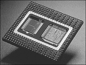
Figure 3.32 Pentium Pro processor with 1MB L2 cache (the cache is in the center and right portions of the die). Photograph used by permission of Intel Corporation.

The main processor die includes a 16KB split L1 cache with an 8KB two-way set associative cache for primary instructions and an 8KB four-way set associative cache for data.
Another sixth-generation processor feature found in the Pentium Pro is the DIB architecture, which addresses the memory bandwidth limitations of previous-generation processor architectures. Two buses make up the DIB architecture: the L2 cache bus (contained entirely within the processor package) and the processor-to-main memory system bus. The speed of the dedicated L2 cache bus on the Pentium Pro is equal to the full-core speed of the processor. This was accomplished by embedding the cache chips directly into the Pentium Pro package. The DIB processor bus architecture addresses processor-to-memory bus bandwidth limitations. It offers up to three times the performance bandwidth of the single-bus, “Socket 7” generation processors, such as the Pentium.
Table 3.19 shows Pentium Pro processor specifications.
Table 3.19 Pentium Pro Family Processor Specifications
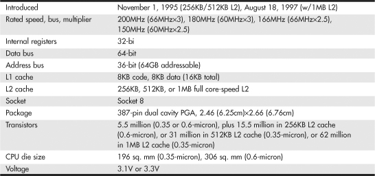
Similar to the Pentium before it, the Pentium Pro runs clock multiplied on a 60/66MHz motherboard. Table 3.20 lists official speeds for Pentium Pro processors and motherboards. There were also unsupported clock multiplier settings of 3.5x and 4x, which if set would result in overclocking the CPU. For example, setting the multiplier to 3.5x on a 66MHz bus would result in 233MHz operation, which worked on many if not most of these processors.
Table 3.20 Speeds for Pentium Pro Processors and Motherboards

The integrated L2 cache is one of the really outstanding features of the Pentium Pro. Because the L2 cache is built into the CPU and is off the motherboard, the Pentium Pro can now run the cache at full processor speed rather than the slower 60MHz or 66MHz motherboard bus speed. In fact, the L2 cache features its own internal 64-bit back-side bus, which does not share time with the external 64-bit front-side bus used by the CPU. The internal registers and data paths are still 32-bit, as with the Pentium. Because the L2 cache is built into the system, motherboards can be cheaper because they no longer require separate cache memory. Some boards might still try to include cache memory in their designs, but the general consensus is that L3 cache (as it would be called) would offer less improvement with the Pentium Pro than with the Pentium. The incorporation of L2 cache is one of the most enduring legacies of the Pentium Pro because this feature has been incorporated into virtually every Intel and AMD processor built since, with the notable exception of the original Celeron.
One of the features of the built-in L2 cache is that multiprocessing is greatly improved. Rather than just SMP, as with the Pentium, the Pentium Pro supports a type of multiprocessor configuration called the Multiprocessor Specification (MPS 1.1). The Pentium Pro with MPS enables configurations of up to four processors running together. Unlike other multiprocessor configurations, the Pentium Pro avoids cache coherency problems because each chip maintains a separate L1 and L2 cache internally.
There are four special VID pins on the Pentium Pro processor. These pins can be used to support automatic selection of power supply voltage. Therefore, a Pentium Pro motherboard does not have voltage regulator jumper settings like most Pentium boards, which greatly eases the setup and integration of a Pentium Pro system. Most Pentium Pro processors run at 3.3V, but a few run at 3.1V.
Pentium II Processors
Intel revealed the Pentium II in May 1997. Prior to its official unveiling, the Pentium II processor was popularly referred to by its code name, Klamath, and was surrounded by much speculation throughout the industry. The Pentium II is essentially the same sixth-generation processor as the Pentium Pro, with MMX technology added (which included double the L1 cache and 57 new MMX instructions); however, there are a few twists to the design. The Pentium II processor die is shown in Figure 3.32.
Figure 3.32 Pentium II Processor die. Photograph used by permission of Intel Corporation.

From a physical standpoint, it was a big departure from previous processors. Abandoning the chip in a socket approach used by virtually all processors up until this point, the Pentium II chip is characterized by its SEC cartridge design. The processor, along with several L2 cache chips, is mounted on a small circuit board (much like an oversized-memory SIMM), as shown in Figure 3.33, and the circuit board is then sealed in a metal and plastic cartridge. The cartridge is then plugged into the motherboard through an edge connector called Slot 1, which looks very much like an adapter card slot.
Figure 3.33 Pentium II processor board (normally found inside the SEC cartridge). Photograph used by permission of Intel Corporation.

The two variations on these cartridges are called SECC (single edge contact cartridge) and SECC2. Figure 3.34 shows a diagram of the SECC package.
Figure 3.34 SECC components showing an enclosed processor board.
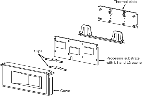
The SECC2 version was cheaper to make because it uses fewer overall parts. It also allowed for a more direct heatsink attachment to the processor for better cooling. Intel transitioned from SECC to SECC2 in the beginning of 1999; all later PII chips, and the Slot 1 PIII chips that followed, use the improved SECC2 design.
By using separate chips mounted on a circuit board, Intel could build the Pentium II much less expensively than the multiple die within a package used in the Pentium Pro. Intel could also use cache chips from other manufacturers and more easily vary the amount of cache in future processors compared to the Pentium Pro design.
Intel offered Pentium II processors with the speeds listed in Table 3.21.
Table 3.21 Speeds for Pentium II Processors and Motherboards

The Pentium II processor core has 7.5 million transistors and is based on Intel’s advanced P6 architecture. The Pentium II started out using a 0.35-micron process technology, although the 333MHz and faster Pentium IIs are based on 0.25-micron technology. This enables a smaller die, allowing increased core frequencies and reduced power consumption. At 333MHz, the Pentium II processor delivers a 75%–150% performance boost, compared to the 233MHz Pentium processor with MMX technology, and approximately 50% more performance on multimedia benchmarks. As shown earlier in Table 3.8, the iCOMP 2.0 Index rating for the Pentium II 266MHz chip is more than twice as fast as a classic Pentium 200MHz.
Aside from speed, the best way to think of the Pentium II is as a Pentium Pro with MMX technology instructions and a slightly modified cache design. It has the same multiprocessor scalability as the Pentium Pro, as well as the integrated L2 cache. The 57 new multimedia-related instructions carried over from the MMX processors and the capability to process repetitive loop commands more efficiently are included as well. Also included as a part of the MMX upgrade is double the internal L1 cache from the Pentium Pro (from 16KB total to 32KB total in the Pentium II).
Maximum power usage for the Pentium II is shown in Table 3.22.
Table 3.22 Maximum Power Usage for the Pentium II Processor
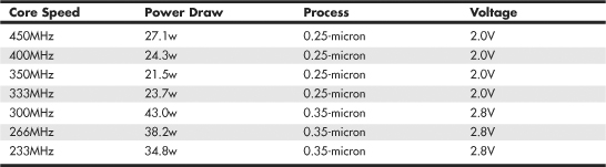
You can see that the highest speed 450MHz version of the Pentium II actually uses less power than the slowest original 233MHz version. This was accomplished by using the smaller 0.25-micron process and running the processor on a lower voltage of only 2.0V. Pentium III and subsequent processors used even smaller processes and lower voltages to continue this trend.
Similar to the Pentium Pro, the Pentium II also includes DIB architecture. The Pentium II processor can use both buses simultaneously, thus getting as much as twice the data in and out of the Pentium II processor as a single-bus architecture processor. The DIB architecture enables the L2 cache of the 333MHz Pentium II processor to run 2 1/2 times as fast as the L2 cache of Pentium processors. As the frequency of future Pentium II processors increases, so will the speed of the L2 cache. Also, the pipelined system bus enables simultaneous parallel transactions instead of singular sequential transactions. Together, these DIB architecture improvements offer up to three times the bandwidth performance over a single-bus architecture as with the regular Pentium.
Table 3.23 shows the general Pentium II processor specifications. Table 3.29 shows the specifications that vary by model.
Table 3.23 Pentium II General Processor Specifications

The L1 cache always runs at full-core speeds because it is part of the processor die. The L2 cache in the Pentium II runs at half-core speed, which saves money and allows for less expensive cache chips to be used. For example, in a 333MHz Pentium II, the L1 cache runs at a full 333MHz, whereas the L2 cache runs at 167MHz. Even though the L2 cache is not at full-core speed as it was with the Pentium Pro, this is still far superior to having cache memory on the motherboard running at the 66MHz motherboard speed of most Socket 7 Pentium designs. Intel claims that the DIB architecture in the Pentium II enables up to three times the bandwidth of normal single-bus processors such as the original Pentium.
By removing the cache from the processor’s internal package and using external chips mounted on a substrate and encased in the cartridge design, Intel could use more cost-effective cache chips and more easily scale the processor up to higher speeds. The Pentium Pro was limited in speed to 200MHz, largely due to the inability to find affordable cache memory that ran any faster. By running the cache memory at half-core speed, the Pentium II can run up to 450MHz while using 225MHz-rated cache chips. To offset the half-core speed cache used in the Pentium II, Intel doubled the basic amount of integrated L2 cache from 256KB standard in the Pro to 512KB standard in the Pentium II.
Note that the tag RAM included in the L2 cache enables up to 512MB of main memory to be cacheable in PII processors from 233MHz to 333MHz. The 350MHz, 400MHz, and faster versions include an enhanced tag RAM that allows up to 4GB of main memory to be cacheable. If you support systems based on the Pentium II, be aware of the caching limitations in the slower processors before upgrading memory above 512MB. Uncached memory will slow down any system.
Pentium III
The Pentium III processor, shown in Figure 3.35, was first released in February 1999 and introduced several new features to the P6 family. It is essentially the same core as a Pentium II with the addition of SSE instructions and integrated on-die L2 cache in the later versions. SSE consists of 70 new instructions that dramatically enhance the performance and possibilities of advanced imaging, 3D, streaming audio, video, and speech-recognition applications.
Figure 3.35 Pentium III processor in SECC2 (Slot 1) and FC-PGA (Socket 370) packages.
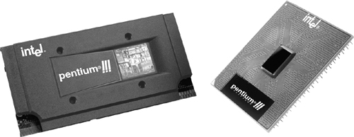
Originally based on Intel’s advanced 0.25-micron CMOS process technology, the PIII core started out with more than 9.5 million transistors. In late 1999, Intel shifted to a 0.18-micron process die (code-named Coppermine) and added 256KB of on-die L2 cache, which brought the transistor count to 28.1 million. The latest version of the Pentium III (code-named Tualatin) uses a 0.13-micron process and has 44 million transistors; motherboards made before the Tualatin-core versions of the Pentium III generally do not support this processor because of logical pinout changes. The Pentium III was manufactured in speeds from 450MHz through 1.4GHz, as well as in server versions with larger or faster cache known as the Pentium Xeon. The Pentium III also incorporates advanced features such as a 32KB L1 cache and either half-core speed 512KB L2 cache or full-core speed on-die 256KB or 512KB L2 with cacheability for up to 4GB of addressable memory space. The PIII also can be used in dual-processing systems with up to 64GB of physical memory. A self-reportable processor serial number gives security, authentication, and system management applications a powerful new tool for identifying individual systems. Because of privacy concerns when the processor was released, you can disable this feature in the system BIOS on most systems that use the Pentium III or Celeron III processors.
Pentium III processors were first made available in Intel’s SECC2 form factor, which replaced the more expensive older SEC packaging. The SECC2 package covers only one side of the chip and allows for better heatsink attachment and less overall weight. Architectural features of the Pentium III processor include the following:
• Streaming SIMD extensions (SSE)—Seventy new instructions for dramatically faster processing and improved imaging, 3D streaming audio and video, web access, speech recognition, new user interfaces, and other graphics and sound-rich applications.
• Intel processor serial number—Serves as an electronic serial number for the processor and, by extension, its system or user. This feature can be enabled or disabled as desired in the BIOS Setup. The serial number enables the system/user to be identified by company internal networks and applications. The processor serial number can be used in applications that benefit from stronger forms of system and user identification, such as the following:
• Applications using security capabilities—Managed access to new Internet content and services; electronic document exchange.
• Manageability applications—Asset management; remote system load and configuration.
Although the initial release of Pentium III processors was made in the improved SECC2 packaging, Intel later switched to the FC-PGA package, which is even less expensive to produce and enables a more direct attachment of the heatsink to the processor core for better cooling. The FC-PGA version plugs into Socket 370 but can be used in Slot 1 with a slot-key adapter.
All Pentium III processors have either 512KB or 256KB of L2 cache, which runs at either half-core or full-core speed. Pentium III Xeon versions have 512KB, 1MB, or 2MB of L2 cache that runs at full-core speed. The Pentium III Xeon is a more expensive version of the Pentium III designed for servers and workstations. All PIII processor L2 caches can cache up to 4GB of addressable memory space and include ECC capability.
Pentium III processors can be identified by their markings, which are found on the top edge of the processor cartridge. Figure 3.36 shows the format and meaning of the markings.
Figure 3.36 Pentium III processor markings.
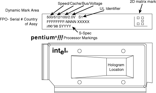
Pentium III processors are all clock multiplier locked. This is a means to prevent processor fraud and overclocking by making the processor work only at a given clock multiplier. Unfortunately, this feature can be bypassed by making modifications to the processor under the cartridge cover, and unscrupulous individuals have been selling lower-speed processors re-marked as higher speeds. It pays to purchase your systems or processors from direct Intel distributors or high-end dealers who do not engage in these practices.
Celeron
The Celeron processor is a chameleon, more of a marketing name than the name of an actual chip. In its first two versions it was originally a P6 with the same processor core as the Pentium II; later it came with the same core as the PIII, then the P4, while more recent versions use the same core as the Core 2 processors. The Celeron name represents essentially a version of Intel’s current mainstream chip that Intel has repackaged for lower-cost PCs.
In creating the original Celerons, Intel figured that by taking a Pentium II and deleting the separate L2 cache chips mounted inside the processor cartridge (and also deleting the cosmetic cover), it could create a “new” processor that was basically just a slower version of the Pentium II. As such, the first 266MHz and 300MHz Celeron models didn’t include any L2 cache. Unfortunately, this proved to have far too great a crippling effect on performance, so starting with the 300A versions, the Celeron received 128KB of on-die full-speed L2 cache, which was actually faster and more advanced than the 512KB of half-speed cache used in the Pentium II it was based on at the time! In fact, the Celeron was the first PC processor to receive on-die L2 cache. It wasn’t until the Coppermine version of the Pentium III appeared that on-die L2 cache migrated to Intel’s main processors.
Needless to say, this caused a lot of confusion in the marketplace about the Celeron. Considering that the Celeron started out as a “crippled” Pentium II and then was revised so as to actually be superior in some ways to the Pentium II on which it was based (all while selling for less), many didn’t know just where the Celeron stood in terms of performance. Fortunately, the crippling lack of L2 cache existed only in the earliest Celeron versions; all of those at speeds greater than 300MHz have on-die full-speed L2 cache.
Since then the Celeron has been released in many different versions, with each newer one based on the then-current mainstream processor. The latest Celerons use the same basic 45nm “Wolfdale” core as more expensive Core 2 processors. The difference is that the Celeron versions are offered in lower processor and bus clock speeds and with smaller caches, in order to justify a lower price point.
Because Intel has offered Celeron and Celeron D processors in many distinctive variations, it’s easy to get confused as to which is which, or which is available at a specific speed. By identifying the spec number of a particular chip and looking up the number on the Intel developer website (http://processorfinder.intel.com), you can find out the exact specification, including socket type, voltage, stepping, cache size, and other information about the chip. If you don’t know the spec number, you can still look up the processor by the model number, or use software such as CPU-Z (www.cpuid.com) to find more detailed information about the processor.
Intel Pentium 4 Processors
The Pentium 4 was introduced in November 2000 and represented a new generation in processors (see Figure 3.37). If this one had a number instead of a name, it might be called the 786 because it represents a generation beyond the previous 686 class processors. Several variations on the Pentium 4 have been released, based on the processor die and architecture. Several of the processor dies are shown in Figure 3.38.
Figure 3.37 Pentium 4 FC-PGA2 processor.

Figure 3.38 The CPU dies for the Pentium 4 CPU based on the Willamette, Northwood, and Prescott cores.
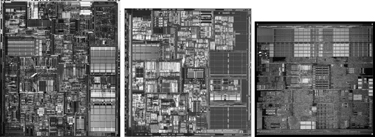
The main technical details for the Pentium 4 include
• Speeds range from 1.3GHz to 3.8GHz.
• Software compatible with previous Intel 32-bit processors.
• Some versions support EM64T (64-bit extensions) and Execute Disable Bit (buffer overflow protection).
• Processor (front-side) bus runs at 400MHz, 533MHz, 800MHz, or 1,066MHz.
• Arithmetic logic units (ALUs) run at twice the processor core frequency.
• Hyper-pipelined (20-stage or 31-stage) technology.
• Hyper-Threading Technology support in all 2.4GHz and faster processors running an 800MHz bus and all 3.06GHz and faster processors running a 533MHz bus.
• Very deep out-of-order instruction execution.
• Enhanced branch prediction.
• 8KB or 16KB L1 cache plus 12K micro-op execution trace cache.
• 256KB, 512KB, 1MB, or 2MB of on-die, full-core speed 256-bit-wide L2 cache with eight-way associativity.
• L2 cache can handle all physical memory and supports ECC.
• 2MB of on-die, full-speed L3 cache (Extreme Edition).
• SSE2-SSE plus 144 new instructions for graphics and sound processing (Willamette and Northwood).
• SSE3-SSE2 plus 13 new instructions for graphics and sound processing (Prescott).
• Enhanced floating-point unit.
• Multiple low-power states.
![]() See “IA-32e 64-Bit Extension Mode (AMD64, x86-64, EM64T),” p. 47 (this chapter).
See “IA-32e 64-Bit Extension Mode (AMD64, x86-64, EM64T),” p. 47 (this chapter).
Intel abandoned Roman numerals for a standard Arabic numeral 4 designation to identify the Pentium 4. Internally, the Pentium 4 introduces a new architecture Intel calls NetBurst microarchitecture, which is a marketing term and not a technical term. Intel uses NetBurst to describe hyper-pipelined technology, a rapid execution engine, a high-speed (400MHz, 533MHz, 800MHz, or 1,066MHz) system bus, and an execution trace cache. The hyper-pipelined technology doubles or triples the instruction pipeline depth as compared to the Pentium III (or Athlon/Athlon 64), meaning more and smaller steps are required to execute instructions. Even though this might seem less efficient, it enables much higher clock speeds to be more easily attained. The rapid execution engine enables the two integer arithmetic logic units (ALUs) to run at twice the processor core frequency, which means instructions can execute in half a clock cycle. The 400MHz/533MHz/800MHz/1,066MHz system bus is a quad-pumped bus running off a 100MHz/133MHz/200MHz/266MHz system clock transferring data four times per clock cycle. The execution trace cache is a high-performance Level 1 cache that stores approximately 12K decoded micro-operations. This removes the instruction decoder from the main execution pipeline, increasing performance.
Of these, the high-speed processor bus is most notable. Technically speaking, the processor bus is a 100MHz, 133MHz, 200MHz, or 266MHz quad-pumped bus that transfers four times per cycle (4x), for a 400MHz, 533MHz, 800MHz, or 1,066MHz effective rate. Because the bus is 64 bits (8 bytes) wide, this results in a throughput rate of 3,200MBps, 4,266MBps, 6,400MBps, or 8,533MBps.
In the Pentium 4’s 20-stage or 31-stage pipelined internal architecture, individual instructions are broken down into many more substages than with previous processors such as the Pentium III, making this almost like a RISC processor. Unfortunately, this can add to the number of cycles taken to execute instructions if they are not optimized for this processor. Another important architectural advantage is Hyper-Threading Technology, which can be found in all Pentium 4 2.4GHz and faster processors running an 800MHz bus and all 3.06GHz and faster processors running a 533MHz bus. Hyper-threading enables a single processor to run two threads simultaneously, thereby acting as if it were two processors instead of one. For more information on Hyper-Threading Technology, see the section “Hyper-Threading Technology,” earlier in this chapter.
The Pentium 4 initially used Socket 423, which has 423 pins in a 39×39 SPGA arrangement. Later versions used Socket 478; recent versions use Socket T (LGA775), which has additional pins to support new features such as EM64T (64-bit extensions), Execute Disable Bit (protection against buffer overflow attacks), Intel Virtualization Technology, and other advanced features. The Celeron was never designed to work in Socket 423, but Celeron and Celeron D versions are available for Socket 478 and Socket T (LGA775), allowing for lower-cost systems compatible with the Pentium 4. Voltage selection is made via an automatic voltage regulator module installed on the motherboard and wired to the socket.
Table 3.24 includes a guide to Pentium 4 processor features as well as those for the Pentium 4 Extreme Edition, which is discussed in more detail in the next section. For information on the features unique to a specific processor, see the Intel Processor Spec Finder at http://processorfinder.intel.com.
Table 3.24 Pentium 4 Processor Information

For some time now, it has been obvious that “Pentium 4” has been far more of a brand than a single processor family, leading to endless confusion when users have considered processor upgrades or new system purchases. Because of the three form factors (Socket 423, Socket 478, and Socket 775) and the wide range of features available in the Pentium 4 family, it’s essential that you determine exactly what the features are of a particular processor before you purchase it as an upgrade to an existing processor or as part of a complete system.
Pentium 4 Extreme Edition
In November 2003, Intel introduced the Extreme Edition of the Pentium 4, which is notable for being the first desktop PC processor to incorporate L3 cache. The Extreme Edition (or Pentium 4EE) is basically a revamped version of the Prestonia core Xeon workstation/server processor, which has used L3 cache since November 2002. The Pentium 4EE has 512KB of L2 cache and 2MB of L3 cache, which increases the transistor count to 178 million transistors and makes the die significantly larger than the standard Pentium 4. Because of the large die based on the 130-nanometer process, this chip is expensive to produce and the extremely high selling price reflects that. The Extreme Edition is targeted toward the gaming market, where people are willing to spend extra money for additional performance. The additional cache doesn’t help standard business applications as well as it helps power-hungry 3D games.
In 2004, revised versions of the Pentium 4 Extreme Edition were introduced. These processors are based on the 90-nanometer (0.09-micron) Pentium 4 Prescott core but with a larger 2MB L2 cache in place of the 512KB L2 cache design used by the standard Prescott-core Pentium 4. Pentium 4 Extreme Edition processors based on the Prescott core do not have L3 cache.
The Pentium 4 Extreme Edition is available in both Socket 478 and Socket T form factors, with clock speeds ranging from 3.2GHz to 3.4GHz (Socket 478) and from 3.4GHz to 3.73GHz (Socket T).
Pentium 4 Power Supply and Cooling Issues
Compared to older processors, the Pentium 4 requires a lot of electrical power, and because of this, starting in February 2000 Intel changed the ATX motherboard and power supply specifications to support a CPU voltage regulator module powered from 12V instead of 3.3V or 5V, as with previous designs. By using the 12V power, more 3.3V and 5V power is available to run the rest of the system and the overall current draw is greatly reduced with the higher voltage as a source. PC power supplies normally generate more than enough 12V power, but the previous ATX motherboard and power supply designs originally allotted only one pin for 12V power (each pin is rated for only 6 amps), so additional 12V lines were necessary to carry this power to the motherboard.
The fix appears in the form of a CPU power connector called the ATX12V connector. Any motherboard having the ATX12V connector requires that you supply power to it. If you are using an older ATX power supply that lacks the proper ATX12V connector, several companies sell adapters that convert a standard Molex-type peripheral power connector to the ATX12V connector. Typically, a 300-watt (the minimum recommended) or larger power supply has more than adequate levels of 12V power for both the drives and the ATX12V connector.
If your power supply is less than the 300-watt minimum recommended, you may need to purchase a replacement supply.
![]() See “Motherboard Power Connectors,” p. 937 (Chapter 18, “Power Supplies”).
See “Motherboard Power Connectors,” p. 937 (Chapter 18, “Power Supplies”).
Cooling a high-wattage processor such as the Pentium 4 requires a large active heatsink. These heavy (sometimes more than 1 lb.) heatsinks can damage a CPU or destroy a motherboard when subjected to vibration or shock, especially during shipping. To solve this problem with Pentium 4 motherboards, various methods have been used to secure the heatsink in the system. Intel’s specifications for Socket 423 added four standoffs to the ATX chassis design flanking the Socket 423 to support the heatsink retention brackets. These standoffs enabled the chassis to support the weight of the heatsink instead of depending on the motherboard, as with older designs. Vendors also used other means to reinforce the CPU location without requiring a direct chassis attachment. For example, Asus’s P4T motherboard was supplied with a metal reinforcing plate to enable off-the-shelf ATX cases to work with the motherboard.
Socket 478 systems do not require any special standoffs or reinforcement plates; instead they use a unique scheme in which the CPU heatsink attaches directly to the motherboard rather than to the CPU socket or chassis. Motherboards with Socket 478 can be installed into any ATX chassis-no special standoffs are required.
Socket T (LGA775) systems use a unique locking mechanism that holds the processor in place. The heatsink is positioned over the processor and locking pins attach it to the motherboard.
Because the Pentium 4 processor family has been manufactured in three socket types with a wide variation in clock speed and power dissipation, it’s essential that you choose a heatsink made specifically for the processor form factor and speed you have purchased (or intend to purchase).
Intel Pentium D and Pentium Extreme Edition
Intel introduced its first dual-core processors, the Pentium Extreme Edition and Pentium D, in May 2005. Although these processors used the code name Smithfield before their introductions, they are based on the Pentium 4 Prescott core. In fact, to bring dual-core processors to market as quickly as possible, Intel used two Prescott cores in each Pentium D or Pentium Extreme Edition processor. Each core communicates with the other via the MCH (North Bridge) chip on the motherboard (see Figure 3.39).
Figure 3.39 The Pentium D and Pentium Extreme Edition’s processor cores communicate with each other via the chipset’s MCH (North Bridge) chip.

For this reason, Intel 915 and 925 chipsets and some third-party chipsets made for the Pentium 4 cannot be used with the Pentium D or Pentium Extreme Edition. Intel’s 945 series, 955X and 975X desktop chipsets, and the E7230 workstation chipset are the first Intel chipsets to support these processors. The nForce 4 series from NVIDIA also works with these processors.
![]() See “Intel 945 Express Family,” p. 221 and “Intel 955X and 975X Family,” p. 222 (Chapter 4, “Motherboards and Buses”), for more information on these chipsets.
See “Intel 945 Express Family,” p. 221 and “Intel 955X and 975X Family,” p. 222 (Chapter 4, “Motherboards and Buses”), for more information on these chipsets.
The major features of the Pentium D include
• Clock speeds of 2.66GHz–3.6GHz
• 533MHz or 800MHz processor bus
• EM64T 64-bit extensions
• Execute Disable Bit support
• 65- or 90-nanometer manufacturing process
• 2MB/4MB L2 cache (1MB/2MB per core)
• Socket T (LGA775)
The 830, 840, and 9xx models also include Enhanced Intel Speed Step Technology, which results in cooler and quieter PC operation by providing a wide range of processor speeds in response to workload and thermal issues.
The Pentium Extreme Edition is a high-end version of the Pentium D, but with the following differences:
• HT Technology is supported, enabling each core to simulate two processor cores for even better performance with multithreaded applications.
• Enhanced Intel Speed Step Technology is not supported.
• It includes unlocked clock multipliers, enabling easy overclocking.
Table 3.25 compares the features of the various Pentium D and Pentium Extreme Edition processors.
Table 3.25 Pentium D and Pentium Extreme Edition Processors

Intel Core Processors
During production of the Pentium 4, Intel realized that the high power consumption of the NetBurst architecture was becoming a serious problem. As the clock speeds increased, so did the power consumption. At the heart of the problem was the 31-stage deep internal pipeline, which made the processor fast but much less efficient. To continue evolving processors with faster versions featuring multiple cores, a solution was needed to increase efficiency and reduce power consumption dramatically. Fortunately Intel had the perfect solution in its mobile processors, already regarded as the most efficient PC processors in the world. Starting with the Pentium M, Intel’s mobile processors used a completely different internal architecture from its desktop processors such as the Pentium 4. In fact, the Pentium M mobile processor was originally based on the Pentium III! To create a powerful new desktop processor, Intel started with the highly efficient mobile processors and then added several new features and technologies to increase performance. These new processors were designed from the outset to be multicore chips, with two or more cores per physical chip. The end result of this development was the Core processor family, which was first released on July 27, 2006 as the Core 2.
Intel Core 2 Family
The highly efficient Core microarchitecture design featured in the Core 2 processor family provides 40% better performance and is 40% more energy efficient than the previous generation Pentium D processor. It is also interesting to note that the Core 2 Duo processor is Intel’s third-generation dual-core processor; the first generation was the Pentium D processor for desktop PCs, and the second generation was the Core Duo processor for mobile PCs.
The naming of both the Core 2 processor and the Core microarchitecture is somewhat confusing because the Core name was also used on the Core Solo and Core Duo processors, which were the successors to the Pentium M in Intel’s mobile processor family. What is strange is that the Core Solo/Duo do not incorporate Intel’s Core microarchitecture, and although they served as a developmental starting point for the Core 2, the Core Solo/Duo are internally different and not in the same family as the Core 2 processors. Because the Core Solo and Core Duo processors are considered mobile processors only, they are not covered here.
The Core 2 was initially released as a dual-core processor, but since then quad-core versions have also been released. The dual-core versions of the Core 2 processors have 291 million transistors, whereas the quad-core versions have double that, or 582 million. They include 1MB or 2MB of L2 cache per core, with up to 8MB total L2 in the quad-core versions. Initially all were built on 300mm wafers using a 65nm process, but since then 45nm versions have been released as well.
The highlights of the Core microarchitecture include
• Wide dynamic execution—Each internal execution core is 33% wider than in previous generations, allowing each core to execute up to four full instructions simultaneously. Further efficiencies are achieved through more accurate branch prediction, deeper instruction buffers for greater execution flexibility, and additional features to reduce execution time.
• Intelligent power capability—An advanced power-gating capability that turns on individual processor subsystems only if and when they are needed.
• Advanced smart cache—A multicore optimized cache that increases the probability that each execution core can access data from a shared L2 cache.
• Smart memory access—Includes a capability called memory disambiguation, which increases the efficiency of out-of-order processing by providing the execution cores with the intelligence to speculatively load data for instructions that are about to execute.
• Advanced digital media boost—Improves performance when executing Streaming SIMD Extension (SSE) instructions by enabling 128-bit instructions to be executed at a throughput rate of one per clock cycle. This effectively doubles the speed of execution for these instructions as compared to previous generations.
The Core 2 family includes both dual-core and quad-core processors under three different names:
• Core 2 Duo—Standard dual-core processors
• Celeron—Low-end single or dual-core processors
• Core 2 Quad—Standard quad-core processors
• Core 2 Extreme—High-end versions of either dual-core or quad-core processors
Figure 3.40 shows a cutaway view of a Core 2 Duo chip, revealing the single dual-core die underneath the heat spreader.
Figure 3.40 Core 2 Duo cutaway view.

All Core 2 family processors support 64-bit extensions, as well as SSSE3 (Supplemental SSE3), which adds 32 new SIMD (Single Instruction Multiple Data) instructions to SSE3. These processors also support Enhanced Intel Speedstep Technology (EIST) and most provide support for hardware Virtualization Technology as well.
Tables 3.26 and 3.27 detail the various processors in the Core 2 family.
Table 3.26 Core 2 Family Dual-Core Processors
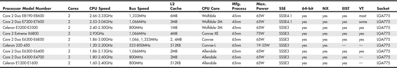
Table 3.27 Core 2 Family Quad-Core Processors

Intel Nehalem (Core i) Processors
The Nehalem microarchitecture is the successor to Intel’s Core 2 microarchitecture. Nehalem processors are known as the Core i Series Family. Key features of this family include the integration of the memory controller into the processor, and in some models, the entire north bridge including an optional graphics processor codenamed Larrabee.
The first Core i Series processor was the Core i7 introduced in November 2008. Initially built on a 45nm process, later Core i Series processors were built on an improved 32nm process allowing for smaller die, lower power consumption and greater performance. All support DDR3 memory and include L3 cache, and some models include support for Hyper-Threading (HT) Technology.
There are two main variants in the Core i Series Family, high end versions that use Socket LGA1366, and more mainstream models that use Socket LGA1156. The latter mainstream models include a fully integrated north bridge including a dual-channel DDR3 memory controller, graphics interface, and even an optional full-blown graphics processor (codename Larrabee). Because the entire north bridge functionality is integrated into the processor, Sockt LGA1156 chips use a slower 2GBps DMI (Direct Media Interface) as the front-side bus connection to the south bridge component on the motherboard.
Core i 900 Series processors using Socket LGA1366 include a triple-channel DDR3 memory controller and a high performance front-side bus called QPI (Quick Path Interconnect) that connects to the north bridge component (called an I/O Hub or IOH) on the motherboard (see Figure 3.41). The IOH implements the PCIe graphics interface.
Figure 3.41 Core i7 900 series processor die. Photograph courtesy of Intel.

The initial members of the Core i Series Family included the Core i5 and i7 processors. These were later joined by the i3 and i9 processors to extend the range on both the low and high-end. Table 3.28 details the various processors in the Core i Series family.
Table 3.28 Core i Series Family Processors

AMD K6 Processors
Unlike Cyrix and some of the other Intel competitors, AMD is a manufacturer and a designer. Therefore, it designs and builds its chips in its own fabs. AMD produced P6-type processors, the initial versions of which were designed to interface with P5 class motherboards for the lower-end markets. AMD later offered up the Athlon and Duron processors, which were true sixth-generation designs using their own proprietary connections to the system.
NexGen Nx586
NexGen was founded by Thampy Thomas, who hired some of the people formerly involved with the 486 and Pentium processors at Intel. At NexGen, developers created the Nx586, a processor that was functionally the same as the Pentium but not pin compatible. As such, it was always supplied with a motherboard; in fact, it was usually soldered in. NexGen did not manufacture the chips or the motherboards they came in; for that it hired IBM Microelectronics. Later NexGen was bought by AMD, right before it was ready to introduce the Nx686—a greatly improved design by Greg Favor and a true competitor for the Pentium. AMD took the Nx686 design and combined it with a Pentium electrical interface to create a drop-in Pentium-compatible chip called the K6, which actually outperformed the original from Intel.
The Nx586 had all the standard fifth-generation processor features, such as superscalar execution with two internal pipelines and a high-performance integral L1 cache with separate code and data caches. One advantage is that the Nx586 includes separate 16KB instruction and 16KB data caches, compared to 8KB each for the Pentium. These caches keep key instruction and data close to the processing engines to increase overall system performance.
The Nx586 also includes branch prediction capabilities, which are one of the hallmarks of a sixth-generation processor. Branch prediction means the processor has internal functions to predict program flow to optimize the instruction execution.
The Nx586 processor also featured a RISC core. A translation unit dynamically translates x86 instructions into RISC86 instructions. These RISC86 instructions were designed specifically with direct support for the x86 architecture while obeying RISC performance principles. They are thus simpler and easier to execute than the complex x86 instructions. This type of capability is another feature normally found only in P6 class processors.
The Nx586 was discontinued after the merger with AMD, which then took the design for the successor Nx686 and released it as the AMD-K6.
AMD-K6 Series
The AMD-K6 processor is a high-performance sixth-generation processor that is physically installable in a P5 (Pentium) motherboard. It essentially was designed for AMD by NexGen and was first known as the Nx686. The NexGen version never appeared because it was purchased by AMD before the chip was due to be released. The AMD-K6 delivers performance levels somewhere between the Pentium and Pentium II processor as a result of its unique hybrid design.
The K6 processor contains an industry-standard, high-performance implementation of the new multimedia instruction set, enabling a high level of multimedia performance for the time period. The K6-2 introduced an upgrade to MMX that AMD calls 3DNow!, which adds even more graphics and sound instructions. AMD designed the K6 processor to fit the low-cost, high-volume Socket 7 infrastructure. Initially, it used AMD’s 0.35-micron, five-metal layer process technology; later the 0.25-micron process was used to increase production quantities because of reduced die size, as well as to decrease power consumption.
AMD-K6 processor technical features include
• Sixth-generation internal design, fifth-generation external interface
• Internal RISC core, translates x86 to RISC instructions
• Superscalar parallel execution units (seven)
• Dynamic execution
• Branch prediction
• Speculative execution
• Large 64KB L1 cache (32KB instruction cache plus 32KB write-back dual-ported data cache)
• Built-in floating-point unit
• Industry-standard MMX instruction support
• System Management Mode
• Ceramic pin grid array (CPGA) Socket 7 design
• Manufactured using 0.35-micron and 0.25-micron, five-layer designs
The AMD-K6 processor architecture is fully x86 binary code compatible, which means it runs all Intel software, including MMX instructions. To make up for the lower L2 cache performance of the Socket 7 design, AMD beefed up the internal L1 cache to 64KB total, twice the size of the Pentium II or III. This, plus the dynamic execution capability, enabled the K6 to outperform the Pentium and come close to the Pentium II and III in performance for a given clock rate.
There were two subsequent additions to the K6 family, in the form of the K6-2 and K6-3. The K6-2 offered higher clock and bus speeds (up to 100MHz) and support for the 3DNow! instruction set. The K6-3 added 256KB of on-die full-core speed L2 cache. The addition of the full-speed L2 cache in the K6-3 was significant because it enabled the K6 series to fully compete with the Intel Pentium III processor family, although it did cause the processor to run very hot, resulting in its discontinuation after a relatively brief period.
The original K6 has 8.8 million transistors and is built on a 0.35-micron, five-layer process. The die is 12.7mm on each side, or about 162 square mm. The K6-3 uses a 0.25-micron process and incorporates 21.3 million transistors on a die only 10.9mm on each side, or about 118 square mm.