
12
Circuit Design and Simulation Using PSpice®
Objectives
Electronic System Design and Manufacturing (ESDM) involves the circuit design, thereby evaluating the circuit performance. Modern integrated circuits on various electronic gadgets such as mobile phones, iPods, and so on need complex circuit design. Hence, the design is done on computers using some software. One such software that is discussed in this chapter is the PSpice software. The features of this software are as follows:
- Design of electronic circuits based on desired performance with trial and error circuit design
- Variation of circuit component parameters for optimum design and cost analysis
- Simulation of possible noise and distortion content to estimate the circuit performance and to study the different methods to overcome such circuit disturbances
- Sensitivity and Fourier analysis without using costly equipment such as spectrum analyzers
- In this chapter basic concepts are explained
12.1 INTRODUCTION
‘SPICE’ means Simulation Program with Integrated Circuit Emphasis. The procedures for setting up of the software are as follows:
- Installation of demo version of PSpice software on a laptop or a personal computer.
- Creation of PSpice schematic (workspace) window.
- Selection of all circuit components and placing them on the workspace of PSpice window.
- Wiring the electronic circuit by interconnecting the total components in the circuit.
- Simulating the circuit response and obtaining the output response for the designed circuit.
12.2 PSPICE WORKSPACE AND WIRING THE CIRCUIT
Steps to work on PSpice to simulate electronic circuits are as follows:
- Install PSpice in the computer.
- Open ‘All Programs’ window on the computer.
- ‘Double click’ on the ICON named as ‘PSpice Design manager’.
- PSpice Design manager window appears (slide 1).
- Select ‘File’ option on the menu bar and click on it.
- Small window drops at it with some options.
- Click on ‘New Workspace’ option.
- Small window pops up showing ‘New Workspace’ on the title bar (Slide 2).
- Enter a name for the ‘input file’ of your choice in the text box under name and click on ‘Create’ menu. In this example, the input file name typed is ‘op amp circuit simulation-1’.
- A new window appears with the following title on its Title Bar (Slide-3). (Page 12-3)
PSpice Design Manager (op amp circuit simulation-1)

Pop-up window to (enter) create a name for the ‘input file’
Example: Enter input filename in the text box as ‘op amp circuit simulation-1’


- Go to ‘Tools’ option on menu bar of workspace window and click on it.
- A small window pops up there with some options on it.
- Double click on ‘Schematic’ option in the small window.
- ‘PSpice Schematics-[Schematic1 p.1]’ window appears as shown in next slide.

PSpice Schematics-[Schematic1 p.1] window
- It consists of total working area for creating an electronic or electrical circuit of our choice of design and obtaining necessary specifications for testing and implementation.
- Electronic circuit design and testing for op amp circuit with voltage gain ‘A’ follows.

Move the mouse pointer on PSpice Schematics-[Schematic1 p.1] window menu bar to option ‘Draw’ and click it. A small window drops at it.

Various steps to create op amp circuit on PSpice schematics window
- The mouse pointer is moved on to the option ‘Get New Part’ on the small window in the previous slide.
- Click ‘Get New Part’ and another small window with the name ‘Part Browser Advanced’ appears.


- Part Browser Advanced window consists of text box with title ‘Part name’.
- Type letter ‘U’ for selecting ‘UA741’ op amp in the text box with Part Name.
- Then the symbol for UA741 op amp appears in the text area with title ‘Library’.
- In the ‘Part List’ text area, UA741 appears as the selected name of the component for the circuit.
Selecting the part ‘op amp’ and placing it in the desired location (area) of ‘op amp’ circuit
- The mouse pointer is moved on to the active button ‘Place’. Click the button ‘Place’ and drag the part symbol to the desired working space to create the circuit. Place (drop) the part symbol.
- Op amp displays the pin numbers 3 (+ terminal) and 2 (− terminal) of input terminals, output terminal (pin 6), and the two supply voltage terminals. Pin 7 to connect + VCC and pin 4 to connect −VCC.

Procedure to identify input AC (VAC) voltage source and fixing its voltage level (Please see the below screen)
- Type VAC in the text box of ‘Part Name’.
- Then AC Voltage source VAC appears in the text area below ‘Library’.
- Click the active button ‘Place’. AC source is selected. Drag the voltage source VAC and place it at desired location at the input port area of op amp UA741. Then the magnitude of voltage source is kept as explained in the first window slide of next page.

Fixing the amplitude of input voltage source VAC for op amp
- Double click ‘0 V’ symbol by the side of input voltage source VAC.
- A small window pops up (appears) with the title bar ‘Set Attribute Value’ and below it another parameter ‘ACMAG’ text box appears with two active buttons ‘OK’ and ‘Cancel’.
- Now type the desired value of voltage to VAC. Type ‘2 V’ in the text area as input amplitude to op amp and click ‘OK’ button now. ‘0 V’ at VAC will be changed to ‘2 V’ as shown in the second slide of this page.

OP amp with input AC voltage source VAC fixed at ‘2 V’ as explained in previous slide

Fixing supply voltages +VCC (15 V) at pin 7 and −VCC (−15 V) at pin 4 of op amp
- Type VDC in the text box of ‘Part Name’ in the window ‘Part Browser Advanced’.
- A DC voltage source appears in the text area nearer to ‘Library’.
- The mouse pointer is moved on to the active button ‘Place’ and clicked. Drag the part symbol ‘DC Voltage Source’ to the desired location nearer to pin 7 of op amp.
- Select another DC voltage source and place it nearer to pin 4, which is nearer to op amp. Set the voltage levels also to +15 V at pin 7 and −15 V at pin 4 of op amp.

Fixing DC voltage sources to + VCC to pin 7 and −VCC to pin 4 of op amp UA741
Procedure to apply supply voltages to op amp is given in the previous slide.

Placing four resistors in op amp circuit
- Placing resistor R1 (1 k) at the non-inverting terminal, resistor R2 (1 k) at the Inverting terminal of input port, resistor RF (10 k) in the feedback path, and resistor RL (10 k) at the output port of op amp as load resistor.
- Type ‘r’ in the text box of ‘Part Name’. Resistor symbol appears in the text area below ‘Library’. Double click the button ‘Place’ and drag the resistor symbol.
- Place the resistor at the non-inverting terminal. Set the value of resistor as R1 and the value as 1 k. Repeat the procedure to place the remaining three resistors at the locations of op amp circuit as shown in the diagram.

- Four resistors R1, R2, RF, and RL are located at various places in the circuit with R1 = 1 k, R2 = 1 k, RF = 10 k, and RL = 10 k according to the various procedures, which are explained till now.
- By now, the required components in the op circuit, UA741, AC and DC voltage sources and resistors are assembled to simulate voltage gain A = 10 in the PSpice simulation process.

Placing ground points for other ends of DC and AC voltages and common ground terminal to total op amp circuit
- Type GND in the text box of ‘Part Name’ in the window ‘Part Browser Advanced’.
- GND symbol appears in the text area nearer to ‘Library’. The GND points are placed at the points as shown in the op amp circuit (shown in next slide).

Five GND points placed at different locations in the op amp circuit
- One op amp UA741, one AC source, two DC voltage sources, four resistors, and five ground points are placed in the circuit.
- Final wiring is done by selecting ‘wire’ from the ‘Draw’ window. After finishing the complete wiring, the circuit is considered to be complete and is ready for testing.

Complete wiring of op amp circuit according to a selected op amp circuit configuration
- By now, the required circuit components are placed at different locations.
- All the components are connected together by wiring. Select ‘Draw’ option on the title bar of ‘PSpice Schematic’ window with input file name ‘op amp circuit simulation-1’ and click ‘Wire’. Then, connecting wires can be drawn on to the workspace area and the total circuit is assembled as shown in the next slide.
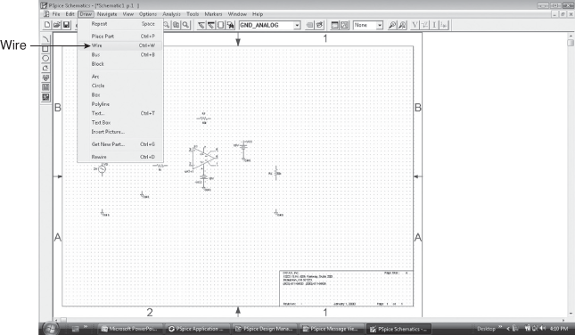
Complete op amp circuit after wiring the total components in the circuit

Testing the stability of wiring of op amp circuit simulation-1
- Move the mouse pointer onto the option ‘Analysis’ on the menu bar of PSpice Schematic (op amp circuit simulation-1) window.
- Then a small window pops down at the selected point.
- Click on the option ‘Create Netlist’. If the circuit wiring is perfect, it will not display anything. Then, we can proceed for simulation and the analysis of the circuit. If there are errors in the circuit, then it displays the errors and they are to be rectified till the netlist becomes zero.

PSpice Message Viewer window appears when we click on ‘Create Netlist’ option on the drop-down window at ‘Analysis’ option (shown below). It displays two messages:
- Creating PSpice Netlist
- Netlist Completed (It does not show any errors in wiring.)
The above two messages indicate that complete wiring of op amp circuit is perfect, and we can go ahead with circuit simulation testing and taking the necessary observations.

- Click on ‘Analysis’ option on menu bar of PSpice Schematic window.
- A small window drops down at ‘Analysis’ location.
- Select ‘Setup’ on the drop-down window and click it. Then a window with the title ‘Analysis Setup’ appears on the screen as shown in the second slide of next page (12–14).

- To obtain simulation output, click Analysis option on the menu Bar of PSpice Schematic window. A small window appears as shown in the previous slide.
- Click ‘Set Up’. Then a window with name ‘Analysis Setup’ appears on it as shown below.
- Select ‘AC Sweep’ and ‘Bias Point Detail’ radio buttons on the Analysis setup window.

Click on Analysis option. Then click ‘Simulate’ option in the drop-down window.

Click on Probe Setup Option and a window appears as shown in the next slide.

In the Probe Setup Options window, select two radio button options:
- Automatically Run Probe after Simulation.
- None

Circuit parameters in Schematics Netlist

Operational amplifier with voltage Gain A = 10, Vin = 2 V, and Vout = 20 V

Input and output voltages of operational amplifier with Gain A = 10

Differential amplifier using op amp UA741
Create circuit file in PSpice Design Manager (differential amp using op amp UA741) window.

Differential amplifier circuit
- Move the mouse pointer onto menu bar and click ‘Tools’ option.
- A small window pops down with options. Click on ‘Schematics’ option.
- A window with PSpice Design Manager schematic-1 p.1 appears. It is shown in next slide.

Differential amplifier using op amp UA741
PSpice Schematics-[Schematic1 P.1] window has the total workspace to create the electronic circuit.

Differential amplifier
- Click on ‘Draw’ option on the title bar of this window.
- Small window pops down as shown below.
- ‘Get New Part’ option in the drop window is used for picking up the total circuit components.
- Wire option is used to join all the selected parts of the circuit for assembling the total circuit.

Differential amplifier using op amp
Clicking on ‘Get New Part’ option, a new window appears with name ‘Part Browser Advanced’.

Differential amplifier using op amp
- Type the first letter of the desired ‘Part Name’ in the text box nearer to Part Name.
- If we need op amp UA741, type the letter ‘U’ in the text box.
- UA741 symbol appears in the text area nearer to Library.
- This part ‘UA741 op amp’ with its pin configuration can be brought into desired place in the workspace of the window as shown in the next window.

Differential amplifier using op amp
- Double click on the active button ‘Place’.
- You find the symbol of op amp at the side of the button area.
- You drag the component (Symbol) and place it (drop) at a convenient place in the workspace area for the circuit.

Differential amplifier using op amp UA741
- Type the letters ‘VAC’ in the text box nearer to ‘Part Name’ (to place voltage source in the op amp circuit at the desired location of ivort of op amp).
- AC Voltage source appears in the text area nearer to ‘Library’.

Differential amplifier using op amp UA741
- Double click on active button ‘Place’ in the ‘Part Browser Advanced’ window.
- Voltage source part appears nearer to the button area.
- Drag the voltage source to the desired location nearer to non-inverting pin 3 of op amp in the workspace and drop (place) at it.
- Using similar procedure, place another voltage source nearer to inverting input terminal ‘2’ of op amp.

Differential amplifier using operational amplifier UA741
- Type VDC in the text box of ‘Part Name’.
- DC voltage source appears in the text area of ‘Library’.

Differential amplifier using op amp UA741
- Place one DC Source nearer to pin 7 to connect +VCC for op amp.
- Similarly, place a second DC Source nearer to pin 4. It should be a negative voltage supply −VCC to op amp. Select the second voltage source and use keys Ctrl+R. The voltage source turns into horizontal direction.
- Again press Ctrl+R keys. Then the voltage source will be rotated by another 90° vertically. Then the voltage source will have its negative terminal in the upward direction.
- Now place the second voltage source nearer to pin 4. Then −VCC can be connected to it (pin 4).

Differential amplifier using op amp UA741
- Type the letter ‘R’ in the text box of Part Name.
- Resistor symbol appears in the text area of ‘Library’.
- Select the resistor and place it nearer to the output port of op amp. The resistor will be in the Horizontal direction. To Use it as load resistor, it should be rotated to vertical direction. Select the resistor and then Use Ctrl+R keys and simultaneously press them. The resistor will turn to vertical direction. Load resistor turned into vertical direction is shown in next slide.

Differential amplifier using op amp UA741
All the circuit components are put on the workspace.

Differential amplifier using op amp UA741
Before doing the total inter connections of the circuit components through ‘wiring’.
- Type GND in the text box in the Part Name area.
- GND appears in the text area of ‘Library’.
- Place the GND at the other ends to DC and AC voltage sources and at common line of op amp. They are shown in the next slide of this page 12-23.

Differential amplifier using op amp UA741
- Select ‘Draw’ option in the Schematics window and click on it.
- Select ‘wire’ option in the pop-down window.
- Use the wire and completely connect the total circuit as differential amplifier as shown in the current slide.

Differential amplifier using op amp UA741
Before verifying for the correctness, the circuit is saved with the file name as shown: Differential amplifier using op amp UA741 on desktop computer.

Differential amplifier using op amp UA741
- Select ‘Analysis’ on the title bar of Schematics window and click it.
- A small window drops down at it.
- Click the option ‘create Netlist’ in the drop-down window.
- If there are no errors in the circuit wiring, then it displays no errors as shown in the next window (Page 12-26).
- If there are any errors displayed, then they have to be corrected till perfect wiring of the circuit is done.

Differential amplifier using op amp UA741
Result comments for perfectness of the assembled circuit without any errors

Differential amplifier using op amp UA741
- To set some values or attributes to input AC voltage source, click on AC source symbol. A small window appears with name ‘V1 part name: AC’.
- It has one text box with Name. Enter VAMPL in it. There will be another text box with name ‘Value’. Enter 2 V in it (or any other convenient value for signal amplitude).
- Click on Save Attribute button and then click ‘OK’ button. The amplitude of the AC signal voltage is set to amplitude of 2 V.

Differential amplifier using op amp UA741
Change the amplitude of the input sine wave using the following sequence of actions:
- Set the amplitude VAMPL = 2 V and click on Save attribute button.
- Click on Change Display button. A small window pops up with name ‘Change Attribute’.
- Click on or select the radio button ‘Both Name and Value’ and click okay.
Sequence of actions −> Enter VAMPL − 2 V −> Save Attr −> Change Display −> Both Name and Value −> Okay

Differential amplifier using op amp UA741
- To set the value of +VCC to 15 V at pin 7 of amp.
- Double Click on ‘0 V’ nearer to DC voltage source. A small window with caption ‘Set Attribute Value’ appears.
- Enter the value of op amp supply voltage in this case for UA741 VCC = 15 V. Then, click on OK on the window. The supply voltage +VCC will be set at +15 V.
- Using the same procedure, set the supply voltage −VCC = 15 V for the second supply terminal at pin 4.
(Please see below slide for details).

Differential amplifier using op amp UA741
- Magnitude of DC power supply voltage +VCC to 15 V at pin 7.
- Magnitude of DC power supply voltage −VCC to −15 V at pin 4 is done by double clicking on ‘0’ and entering the value 15 V in the text box of set value window appeared on it.

Differential amplifier using op amp UA741
- Double clicking ON value 1 k by the side of resistor R1, a small window appears with caption: Set Attribute value.
- Enter 15 k in the text box.
- Save the attribute and click on OK.
- Now the value of the resistor is set at 15 k.
- Using the same procedure, change the name of the resistor R1 as RL to indicate that it is a load resistance RL.

Differential amplifier using op amp UA741
- Double click on resistor parameter R1. Small window with caption ‘Edit Reference Designator’ appears on the screen.
- Enter ‘RL’ in the text box and click OK. Name of the resistor will be changed to RL now.

- Differential amplifier circuit using op amp UA741
- Final circuit to process the result (output Vout)

Differential amplifier with feedback

Summing amplifier circuit using op amp UA741
Vin1 = 5 V, Vin2 = 2 V, and resulted output Vout = −7 V

Summing amplifier using op amp UA741
Input voltage Vin(1) = 5 Volts, Vin(2) = 2 Volts, and output result Vout = −7 V

Summing amplifier with feedback resistor changed to 22 k

Output response of summing amplifier with feedback resistor RF = 22 k
Vin1 = 5 V, Vin2 = 2 V, Vout = −15 V

Summing amplifier using op amp UA741

Input and output voltages of summing amplifier using op amp UA741
Vin1 = 10 Volts, Vin2 = 2 Volts, and output Vout = 8 Volts

Circuit diagram of a subtractor using op amp UA741

Input and output voltages of a subtractor using op amp 741 Vin1 = 8 V, Vin2 = 5 V, and Vout = 3 V

Circuit diagram of a comparator using op amp UA741

Input and output waveforms of a comparator using op amp with Vin = 5 V, Freq = 1 kHz, and Vref = 4 V

Circuit diagram of active low-pass filter using op amp UA741

Input and output waveforms of active low-pass Filter using op amp UA741

Circuit diagram of active low-pass filter using op amp UA741

Frequency response for active low-pass filter using op amp

Circuit diagram of first-order low-pass filter using op amp UA741 with R = 560 ohm and C = 0.1 μF

Frequency response of first-order low-pass filter using UA741 with R = 560 ohm and C = 0.1 μF

Circuit diagram of first-order low-pass filter using op amp UA741 with R = 15.9 kohm and C = 0.01 μF

Frequency response of first-order low-pass filter using op amp UA741 with R = 15.9 kohm and C = 0.01 μF

Operational amplifier with voltage Gain A = 10, Vin = 2 V, and Vout = 20 V
(Please see pages 1 to 20 to know the total procedure to assemble the circuits.)


Input and output voltages of operational amplifier UA741 with Gain A = 10

Summing Amplifier using op amp UA741

Input and output value of Summing Amplifier using op amp UA741

High-pass filter

High-pass filter response

High-pass filter

High-pass filter

High-pass filter response

Wideband pass filter using op amp

Frequency response of wideband pass filter

Notch filter using op amp

Frequency response of notch filter

Cadence, the Cadence logo, Allegro, and OrCAD are registered trademarks of Cadence Design Systems, Inc. in the United States and other countries. All other trademarks are the property of their respective owners. For more information about OrCAD or PSpice please write to [email protected].