11
Introduction to Digital Integrated Circuits
Objectives
To understand the theory, analysis, and basic concepts of digital integrated circuits
- Integrated circuits
- Various logic gates
- Logic gates using bipolar junction transistors as switches.
- Inverter, AND, NAND, OR, and NOR gates using BITs
- Logic gates using MOSFETs as electronic switches
- Inverter, AND, NAND, OR, and NOR gates using MOS and CMOSFETs
- Introduction to digital integrated circuits
11.1 INTRODUCTION TO INTEGRATED CIRCUITS
Knowledge about different types of integrated circuits (ICs), along with their applications and usage in computer circuits, microcontrollers, microprocessors, and programmable logic arrays are important for engineers of all disciplines (Computer, Electronics, Electrical, Civil, and Mechanical). Present day Engineers have no choice but for learning both hardware and software technologies because they are used in all forms of advancements of their individual disciplines.
- An integrated circuit is also known as IC, microcircuit, microchip, silicon chip, or chip. It is a miniaturized electronic circuit consisting of semiconductor devices and passive components. Integrated circuit is a complex electronic structure, in which multiple electronic components are embedded into a small package. Transistors, diodes, resistors, and capacitors can be integrated into an IC in large quantities, up to tens of millions of devices in microprocessors and programmable logic arrays.
- Depending on the input and output signals (analog/digital), ICs are broadly classified as follows:
- Analog integrated circuits: Amplifiers, voltage regulators, filters, convertors, etc.
- Digital integrated circuits: Logic gates, counters, flip-flops, microprocessors, etc.

- 3. Integrated circuits are used in electronic gadgets that we use in day- to-day life, such as an alarm clock that wakes us up, TV that shows daily news and radios, and mobile phones to talk to people from all over the world. This fast growing civilization is delivered all over the world due to the launch and rapid development and deployment of the ICs in various advanced applications.
Main Advantages of ICs
- Low in cost (laws of scale)
- Small and compact in size
- Low in mass and weight
- Large-scale production due to the batch processing of large number of devices and components
- Components are reliable
- Matched transistors available for specific applications
- Low power requirement, resulting in low voltage operation of mobile devices such as cell phones and tablets
- Easily programmable
- Limitations of IC
- Inductors and transformers cannot be fabricated on ICs
- If any internal component of the IC goes out of order, the entire chip has to be replaced
- Capacitors and resistors are limited in maximum values
- High power ICs cannot be produced (greater than 10 W)
11.2 CLASSIFICATION OF INTEGRATED CIRCUITS
Digital ICs are classified as follows:
- Fabrication techniques
- Functionality
- Number of gates inside an IC
- Active devices employed in IC
Fabrication Techniques
On the basis of fabrication techniques, the ICs can be classified as
Monolithic ICs
In monolithic IC, the active and passive elements and their circuit layouts with interconnections are formed upon or within silicon wafers. Monolithic ICs are most common type used in our daily life. Commercially available monolithic ICs are amplifiers, voltage regulators, AM receiver, TV circuits, etc.
Hybrid ICs
When an IC consists of a number of monolithic ICs, then the combination is known as hybrid IC. Hybrid ICs are widely used for high-power audio amplifier applications.
Thin and Thick Film ICs
Due to the use of printing technique in their silk screen process, they are also known as film printed circuits. These ICs have the advantage of forming passive components with wider range of values, better tolerances, and better isolation between the components when compared to monolithic ICs.
Functionality
On the basis of functionality, IC can be divided into two classes.
- 1. Linear IC: For linear ICs, input and output relationship of a circuit is linear; they are used in making amplifiers, oscillator circuits, etc.
- Digital IC: When a circuit is either in ON state or OFF state and not in between the two states, the circuit is known as a digital circuit. These digital ICs are used for logic operations and used in computers, logic circuits, digital communication systems, etc.
Scale of Integration
- Small-scale Integrated (SSI) Circuits: These circuits contain only few tens of transistors; and their typical applications are operational amplifiers and logic gates. During 1962s, Apollo programme and Minuteman Missile-based defence programme used SSI chips. The average price of a chip fell from $50 in 1962 to $2 in 1968.
- Medium-scale Integrated (MSI) Circuits: These circuits contain few hundreds up to 1,000 of transistors; these circuits include counters and registers.
- Large-scale Integrated Circuits (LSI) (mid-1970s): They contain of more than 1,000 transistors on a single chip; they were typically used in 1 kB RAM, calculator, and first microprocessors (using 4,000 transistors).
- Very Large-Scale Integrated (VLSI) Circuits (early 1980s till late 2000s): These circuits contain more than 100,000 transistors on a single chip. Their typical applications are FPGA and CPU.
- Ultra Large-Scale Integrated (ULSI) Circuits: These are used with integrated systems using millions to billions of transistors per chip.
- 6. Wafer-Scale Integrated (WSI) Circuits: These circuits are used for large-scale systems in super computers. Because of the large-scale production of large systems, system costs are reduced.
- 7. System ON Chip (SoC or SOC) Circuits: comprises of total circuit design and assembling of all disparate components of sub-system or sub-systems into a single chip, so as to simplify overall system design. Quite useful in smaller digital systems such as mobile phones (with very large volume) which carry a computer subsystem on a SOC. Though the design and manufacturing of SOC is complex, its final chip reduces power consumption and also the overall cost of the end devices. SOC consists of hardware and Software Typical application is embedded Systems.
- 8. Three-dimensional Integrated Circuits (3D-ICs): They have two or more layers of electronic components that are designed into vertical or horizontal layers, enabling communication between the layers within the circuit die. This type of IC further simplifies the overall gadget design.
Devices Employed in IC
Nanotechnology in present-day IC fabrication suggests the existence of billions of transistors in an IC.
On the basis of device fabrication technology, ICs can be classified as
- Bipolar ICs: They use bipolar junction transistor (BJT)
- Unipolar ICs: These circuits use field-effect transistor (FET) and MOSFET
Two techniques are used for the manufacture of ICs namely bipolar and metal oxide semiconductor (MOS) technologies.
- Bipolar technology is preferred for SSI and MSI because BJTs work faster.
- Metal oxide semiconductor technology is preferred for LSI because of the increased density of MOSFETs in same chip area.
There are many types of integrated logic circuits, also called as logic families, and they are classified as
- Bipolar logic families use bipolar devices such as diodes and transistors, along with passive elements such as resistors and capacitors.
- Unipolar logic families use unipolar devices such as MOSFETs in addition to passive elements.
11.3 CLASSIFICATION OF LOGIC FAMILIES
The hardware technology used to build logic circuits electronically is introduced in this chapter. Further, fundamental building blocks to implement large-size electronic circuits are familiarized step by step. Standard logic gates contain hundreds of transistors to implement simple logic function.
Bipolar Logic Families
In bipolar ICs, there are mainly two types of logic operations:
- Saturated logic
- Unsaturated logic
The difference between saturated and unsaturated logic circuits is that in the former, the transistors used in the IC are driven to function in the saturation region of device characteristics, while in the latter, the transistors are not driven into the saturation region.
Examples of saturated logic:
- Resistor transistor logic (RTL)
- Direct coupled transistor logic (DCTL)
- Integrated injection logic (IIL or FL)
- Diode–transistor logic (DTL)
- High threshold logic (HTL)
- Transistor–transistor logic (TTL)
- Metal oxide semiconductor (MOS) logic
- Complementary MOS (CMOS) logic
Examples of unsaturated logic family are as follows:
- Schottky TTL
- Emitter-coupled logic (ECL)
Unipolar Logic Families
MOSFETs are used in unipolar logic ICs. The different types of MOSFET’s used are as follows:
- N-channel MOSFETs
- P-channel MOSFETs
- Complementary MOSFETs that employ both P-channel mosfet and N-channel mosfet devices on the same chip.
Accordingly, the unipolar logic families are classified as in the following:
- PMOS
- NMOS
- CMOS
11.3.1 Introduction to Logic Gates
Logic gates are mostly used in the design of large complex ICs such as microprocessors and computers. Digital systems and ICs using binary logic signals are known as digital logic families. In digital electronic systems, information carrying data, audio, and video are processed in their binary form, where all of the information is encoded in two-valued binary values 0 and 1. However, processing such binary data requires binary logic circuits to conduct various logic operations (these are different from the typical decimal operations). The input and output voltages (currents) of digital electronic circuits contain this binary data. Boolean algebra is used for the design and analysis of digital electronic systems. The two states of binary logic variables can be represented in different styles of logic operations based on logic levels.
- ON or OFF
- TRUE or FALSE
- Open or Closed
- HIGH or LOW
Example for ON/OFF state representation is an electronic switch. When a transistor/FET conducts, it is in the ON state; further, when the transistor’s output voltage is ‘LOW’ (ranging from 0 to 0.8 V), it is considered as value ‘0’. Similarly, if the transistor is in the OFF state, output voltage is ‘HIGH’ (ranging from 2 to 5 V), it is considered as value ‘1’. Based on this definition of ‘electronic switching’ of ON and OFF states, BJT, FET, MOSFET, and CMOSFET are used in logic circuits to form digital electronic systems.
Logic/binary data is denoted by 0s and 1s for binary mathematical operations that are implemented using electronic devices and resistors in building blocks called ‘logic gates’. Their structure and architecture depends upon the required logical mapping and electronic applications. The simplicity or complexity in the architecture (layout) of logic gates goes hand in hand with their use in many commonly known applications such as follows:
- mobile phones/tablets/smart phones/phablets
- arithmetic logic units (ALU), central processing units (CPU), memory chips (RAM/ROM), and controls in computer circuits
- digital communication systems
- automobile circuits
Complex systems and applications (state machines) are solved by dividing them into smaller and smaller sub-operations (software applications running on top of the operating system which in turn runs on microprocessors, with higher computer languages translating into binary code and logic) in binary/Boolean logic.
Three fundamental/basic logic gates (building blocks) using Boolean algebra with values 0s and 1s are AND gate, OR gate, and NOT gate. Boolean algebra was invented by G. Boole to solve logic equations using only two values (0 and 1), instead of the traditional binary system (0 to 9).
The basic logic gates are extended into four more logic operations: NAND, NOR, EX-OR, and EX-NOR. Further, two logic gates NAND and NOR are known as universal gates, meaning the combination of these gates can effectively solve large complex logic functions/operations. Two most popular minimization techniques are Karnaugh Maps and Quine–McCluskey methods.
These logic gates are used directly or in various combinations to form the root operations in Digital Electronics and Telecommunication engineering. They use broadly sequential or combinational switching circuits. The understanding of complex digital circuits becomes easier, once the fundamental concepts are clear in mind.
Most of the digital electronic systems use ICs. Some ICs with logic gates are shown in the following discussions to familiarize with practical circuit assembly. However, logic operations in digital circuits use ICs fabricated using different technologies such as transistor–transistor logic (TTL) circuits using BJTs, NMOSFET devices and resistors using MOSFETs, and complementary metal oxide semiconductor (CMOSFET) devices, and resistors using MOSFETs.
11.3.2 Concepts of AND, OR, and NOR Logic Gates
Definition of AND Logic Gate
Figure 11.1(a) and (b) show two-input AND gate and three-input AND gate, including their graphical symbols and truth tables. A truth table indicates the status of output voltage for different combinations of input voltages (currents) to the logic gate circuit; further, it shows the logic functions performed by the individual logic gates on its input and output signals.


Fig. 11.1 (a) Two-input AND and (b) Three-input AND Gates

Fig. 11.1 (c) 7408 IC Quad Two-input AND Gates
Operation of AND Logic
For two-input AND gate, output Y is TRUE (1) if and only if both the inputs (A and B) are TRUE (1). It can take two or more inputs and gives out a single output.
AND Gate: Logic Operations of Two-input and Three-input AND Gates
Figure 11.1(a) shows the two-input AND gate operation with two inputs A and B and output Y with their corresponding symbol and truth table, containing its input and output states (logic functions). Output Y is a function of the two input variables A and B. The binary/Boolean logic operation of AND gate is Output Y = Input A· Input B.
This expression can be extended to include multiple inputs. Output Y = (A·B·C…N) for N-inputs.
Three-input AND Gate
Three-input AND gate symbol and truth table are shown in the Fig. 11.1(b). Output ‘Y’ is a function of three input variables A, B, and C as shown in the truth table, with output Y = A · B · C. This is similar to a simple multiplication operation. Output will be equal to 1 only when all its inputs are in ‘1’ state. If any one of the inputs is in ‘0’ state, the output becomes ‘0’.
Commercial ICs Performing Logic Operations
Following table has a list of commercial ICs that perform specific logic functions, and this chapter will discuss the first four of the listed ICs.

The IC 7408 has four AND gates and Fig. 11.1(c) shows the IC along with the pin configuration.
Two-input Quad AND Gate IC 7408
Definition of OR Logic Gate
Two-input and three-input OR gate operations are shown in Fig. 11.2(a) and (b), along with symbols and their truth tables.


Fig. 11.2 (a) Two-input; (b) Three-input OR Gate; (c) NOR Gates and (d) IC 7402 Quad NOR Gate
Output Y = Input A + Input B
OR logic is used in a system, where output is enabled/TRUE when any one of the input is TRUE.
The logic operations or equations of OR gate follow the simple rules of binary addition. (Note: the normal operation of addition is given as (1 + 1 = 2), whereas in binary/Boolean operation of OR will be (1 + 1 = 1).)
Logic Operation of OR Gate
For two-input OR gate, output Y is TRUE (1) if
- Input A is TRUE (1) or input B is TRUE (1), or
- both input A and input B are TRUE (1)
It can be extended to any number of inputs and can operate on multiple inputs and produce a single output.
Logic equations for two-input OR operation and three-input OR operations are shown in Fig. 11.2(a) and (b).
Definition of NOR Logic Gate
The symbol of NOR gate and the corresponding truth table are shown in Fig. 11.2(c). Further, IC 7402 with quad (four) NOR gates is shown in Fig. 11.2(d). From the logic operations shown in the truth table, it can be observed that the NOR gate operation is a combination of AND, NOT, and OR logic operations. NAND gates and NOR gates are mostly used in solving Boolean equations and implementing digital electronic circuits.
11.3.3 Concepts of NOT, NAND, Exclusive-OR (XOR) Logic Gates
The symbol of NOT logic gate (inverter) circuit, IC 7404 (commercial IC), and the corresponding truth table are shown in Fig. 11.3(a) and (b) respectively.

Fig. 11.3 (a) Symbol of NOT Gate (Inverter) Circuit; (b) Pin Configuration of 7404 HEX Inverter IC; and the Corresponding Truth Table
Logic Operation of NOT/Inverter
The output voltage levels of NOT/inverter gate represent inverse or complement operation to input signals. The NOT circuit inverts an input signal. At the same time, binary signal levels and the wave shapes of voltages do not undergo any changes during the transmission through gates. The inverter circuit operates on one input voltage Vin [signals shown in Fig. 11.3(a)].
- When input voltage Vin = OFF (0) state, output voltage Vout = ON (1) state.
- When input voltage Vin = ON (1) state, output voltage Vout = OFF (0) state.
Behaviour of NOT Gate
Single-input NOT gate with its symbol and their truth table are shown in Fig. 11.3(a) and (c).
NOT Operation: In this operation, output Y equals NOT of A. In other words, output Y is the complement of A. It means that if A = 0, its output Y = 1 and vice versa. The inverter/NOT circuit operates with single input and single output only.
Behaviour of NAND Gate
NAND Gate: NAND operation is a combination of NOT and AND operations in a single module of AND and NOT circuit, as shown in Fig. 11.4(a) and (b). From the logic operations shown in the truth table, NAND gate operation is a combination of OR, AND, and NOT logic operations.

Fig. 11.4 (a) Two-input NAND Gate; (b) Another Representation of Two-input NAND Gate with Another and (c) 7400 IC Quad Two-input NAND Gates
Logic Equations for Two-input and Three-input NAND Operations
NAND operation is self-explanatory from its symbols shown in Fig. 11.4(a); further, the corresponding truth table is given in Fig. 11.4(b). IC 7400 having four two-input NAND gates is shown in Fig. 11.4(c), along with its logic operations.
Definition of Exclusive-OR Gate Behaviour
The output level of two-input ‘Exclusive OR’ gate will be in ‘1’ state, if only one of the inputs assume the state ‘1’ (this means that if both inputs are ON, then the output is going to remain as OFF).
Exclusive-OR Gate: Logic Equations and Truth Table for Two-input X-OR
Exclusive-OR gate symbol and the corresponding truth table are shown in Fig. 11.5(a). The operation of Exclusive-OR can be explained as when output Y is TRUE, if input A is TRUE (1) or input B is TRUE (1) with a constraint such that the condition of truth is exclusive. In other words, input A and input B should not remain TRUE (1) at a time when output Y of Exclusive-OR gate has to be TRUE.


Fig. 11.5 (a) The Symbol of Exclusive-OR Gate and Boolean Expression Y = A + B, and Truth Table of Exclusive-OR Gate
Sample Applications
Digital computers and computer programming use logic circuits for arithmetic operations such as addition, subtraction, multiplication, and division. Multiplication is repeated addition, while division is repeated subtraction. Flip-Flop circuits can also be realized using NOT gates, and they are used in memory and register circuits.
Any arbitrary function can be synthesized by using a combination of logic gates such as AND, OR, NOT, NOR, or NAND. An example for the synthesis of logic network using the function:
Output Y = ABC + (A + B + C) + BC
Example 11.1
Consider the following Boolean expression;
Output Y = ABC + (A + B + C) + BC
where A, B, and C are the inputs.
Select the required logic gates and draw a logic network for implementation and layout.
Solution: From the individual logic gate circuit diagrams, the output logic levels can be predicted from the nature of inputs to the digital system using Boolean algebra. From the total digital circuit diagram, required Boolean expression can be predicted by simple observation.
The expression is divided as follows:
- Two product terms ABC and BC are implemented by using two AND gates.
- The function (A + B + C) can be implemented by using one OR gate.
- In order to realize total output ‘Y’, outputs of the three gates (two AND and one OR) are applied through another OR gate.
Thus, Fig. 11.5(b) shows the logic gate circuit for Boolean expression

Fig. 11.5 (b) Implementation of Boolean Expression Using Logic Gates
Y = ABC + (A + B + C) + BC.
Instead of using separate OR and AND gates, the Boolean expression can also be simulated by using NAND and NOR gates.
Example 11.2
Simulate the function of a ‘logic network’ to provide output Y = (A · B′ + C · D), where A, B, C, and D are the input signals.
Solution:
- B′ can be implemented by using one inverter, and term A · B′ implemented by using one AND gate.
- Term C · D can be implemented by using one AND gate.
- Total output Y can be implemented by using OR gate using the two outputs of the above gates as two inputs.
- Therefore, output Y = (A · B′ + C · D). The simulation of logic network for Boolean expression is shown in Fig. 11.5(c).

Fig. 11.5 (c) Implementation of Boolean Expression Using Logic Gates
11.3.4 Comparison of Various Logic Families
- Power supply requirements of the circuit
- Reliability of the circuit
- Maintainability of the circuit
- Cost of the circuit
- Past history in electronic circuit applications
- Propagation time delay for switching between logic states (speed)
- Interfacing capabilities with other circuits in the chain, which are measured by fan-in and fan-out capabilities
- Immunity to noise levels
- Over-all power dissipation in a package
- Logic configurations and their implementations on VLSI vary depending upon the applications
Diode–Transistor Logic Circuit: Three-input NAND gate DTL circuit is shown in Fig. 11.5(d). It consists of three diodes, one transistor, and two resistors for multiple inputs A, B, and C for a single output ‘Y’. (DTL circuits have current hogging, propagation delay, and voltage degradation; hence, they are not used in latest IC applications.)

Fig. 11.5 (d) Three-input Diode Transistor Logic Circuit to Explain the Circuit Operation Principles
Working Operation of Circuit
- If the input voltage to any of the inputs A, B, or C is in a LOW state (zero voltage), the corresponding diode will conduct. The transistor will be switched OFF and then output voltage Y will be in HIGH state (logic 1)
- If the input voltages to all the three inputs are in LOW states, all the three diodes will conduct by turning off the transistor. Then, the output of the NPN transistor will be in HIGH state (logic 1)
- If the voltages to all the three inputs A, B, and C are in one (1) state (HIGH), the diodes will not conduct, because all the diodes are reverse biased. The transistor is turned ON due to the supply voltage and the DC biasing voltages. Transistor output voltage ‘Y’ will be in LOW state (logic 0).
Such logic operations show that it is an NAND gate. Presently, diode transistor circuits are not used, due to the main disadvantages such as limited speed operation and less noise immunity. Therefore, TTL circuits evolved with many advantages.
Transistor–Transistor Logic
The speed limitation in DTL is remedied in TTL gate circuit. A simple TTL gate circuit is shown in Fig. 11.6(a). The TTL logic family gates are available to implement most of the Boolean functions in SSI and MSI ICs. Digital circuits can be synthesized with TTL gates.

Fig. 11.6 (a) Transistor–Transistor Logic Circuit
Let us analyse the operation of the TTL circuit as in the following:
- Consider input A to transistor T1 be logic ‘1’ (HIGH). Then, the emitter–base junction of NPN transistor T1 is reverse biased. While, collector–base junction of transistor T1 is forward biased by
- the supply voltage. Therefore, current I(B1) flows through ‘R’, through base–collector junction of T1, into the base of transistor T4 and transistor T4 conducts. Therefore, output voltage Vout will be ‘LOW’.
- Consider input A to transistor T1 be logic ‘0’ (LOW). Then, the emitter–base junction of NPN transistor T1 is forward biased. The charge stored in the base of T4 is removed very fast through the collector of transistor T1. Transistor T4 switches very fast into OFF state, with the output voltage changing to HIGH (logic 1) state.
- If DTL and TTL circuits are compared, resistor RB is absent in TTL logic circuit. Hence, TTL logic circuits work at faster speeds and do not lose amplitude and are used extensively in present-day technologies.
11.4 STANDARD TTL NAND GATE: ANALYSIS AND CHARACTERISTICS
The TTL belongs to saturated bipolar transistor logic family. The TTL circuits has become popular and have been widely used for a long time. Therefore, they are considered as ‘standard TTL gates’, and the circuits use only transistors. However, the TTL circuit is an improved version of resistor–transistor logic (RTL) and DTL circuit families. In Fig. 11.6(a), the single-input TTL logic circuit layout is used as a single logic gate, and if this circuit needs to be expanded to provide multiple input signals in the logic, the following process is adopted.
Multiple inputs can be provided by using paralleled transistors with input base, emitter, and collector terminals connected, as shown in Fig. 11.6(b), to meet the circuit requirements. The modified circuit layout is shown in Fig. 11.7.

Fig. 11.6 (b) Transistor–transistor Logic NAND Gate with Input Transistor T1 with Base Terminals Tied Together and Collector Terminals Tied Together to Understand the Concept of Multiple Emitter Transistor T1 in Fig. 11.7

Fig. 11.7 Transistor–transistor Logic Circuit with Multiple Emitters for Three Inputs
Operation of Multiple Emitter Transistor Circuit
The operation of multiple emitter transistor can be clearly understood by considering a basic circuit with three transistors, as shown in Fig. 11.6(b). The features of the circuit are that three base terminals of the three transistors are tied together, three collector terminals are tied together, and input voltages are applied between emitter terminal of each transistor and ground or common terminal.
Instead of using paralleled transistor structure shown in Fig. 11.6(b), single transistor with multiple emitters (to operate on multiple inputs as required in logic gates) with common base and common collector structure is used nowadays, as shown in Fig. 11.7. In IC fabrication, creating such transistors with multiple emitters is more convenient. The transistor with multiple emitters in logic gates is further discussed in the following.
Transistor–transistor logic (TTL) gate circuit with multiple emitters is shown in Fig. 11.7.
From the figure, we can observe that the TTL gate work with three inputs. Multiple-emitter transistor has three emitters to operate with three input signals A, B, and C, working as three-input NAND gate. Further, the truth table for the NAND gate is given in Table 11.1.
Table 11.1 Truth Table for Triple Three-Input NAND Gate Shown in Figs. 11.6 and 11.7

If any one of the signal level or all the three-input signal levels to transistor T1 are at logic level ‘0’ or LOW, input transistor–emitter junction(s) is forward biased, and transistor T1 conducts. As a result, the output voltage of transistor T1 goes LOW. Further, the low output voltage of transistor T1 is connected/transmitted to the base terminal of transistor T4, which is switched into OFF condition. Then, output voltage Y will turn to logic ‘1’ state.
If all the three logic inputs A, B, and C to the NAND gate are maintained at ‘HIGH’ (1) state, the emitter junctions of transistor T1 are reverse biased, making the transistor to be in ‘OFF’ condition. The collector voltage of transistor T1 will be in ‘HIGH’ (1) state. This high voltage is communicated to the base terminal of transistor T4, turning it into ‘ON’ state. Then, output voltage Y will be ‘0’. This implies the logic ‘0’ state of NAND gate, when all its input voltages are in logic ‘1’ condition.
The TTL NAND gate is discussed till now without considering the associated junction capacitances in BJTs. The inherent junction capacitance (present at the output port of second transistor T4) results in propagation delays: propagation delay during the signal transmissions from LOW to HIGH state (PDLH) and propagation delay during the signal transmissions from HIGH to LOW state (PDHL). Such propagation time delays occur during the transitions of LOW to HIGH states or HIGH to LOW states at the output levels in the logic gates.
Three-input NAND Gate with Totem-pole Circuit Operation
The propagation delays during the transitions of output logic voltage levels ‘0’ and ‘1’ are minimized by using totem-pole output circuit, which uses two transistors T3 and T4. Totem-pole circuit uses a phase splitter circuit (using transistor T2) for switching ON and OFF operations between the two transistors T3 and T4 at a time. Texas Instruments started the manufacture of these TTL family of logic gates since the early years of 1960s.
The propagation delays for output logic level transitions are due to the large charging time constant (Rc × Cout) at the output port of the NAND gate. Further, the transition times between the logical switching can be minimized by reducing the component value of collector resistor of transistor T4. But reduction in Rc increases the Collector current with consequence in increased power dissipations in the resistor Rc and the transistor T4.

Fig. 11.8 Three-input TTL NAND Gate with Phase Splitter and Totem-pole Output Circuits
To avoid such undesirable situation of increased power dissipation, an emitter follower circuit to simulate low value of Rc and diode D1 is introduced in the circuit in place of original Rc. Transistor T4 will be in ON state, when the transistor T3 is in OFF state. Such switching operations are achieved by using a phase splitter circuit using transistor T2. The low value of output resistance of emitter follower circuit (using transistor T3) takes care of the minimization of propagation delays and avoids the increase in power dissipation in the transistor.
T3 is an NPN transistor and forms an emitter follower circuit. When the output voltage is ‘LOW’, emitter (input) junction of T3 is reverse biased due to the voltage drop across diode D1. Transistor T3 will not conduct and transistor T4 only conducts, thus making the output resistance very low.
When the output is HIGH, transistor T3 conducts and the output resistance is very low. Therefore, we have low output resistances for both HIGH and LOW states of transitions. The charge and discharge time constants are low, resulting in low propagation delays in the circuit.
11.4.1 Two-input TTL NAND Gate
Circuit Description
- Standard two-input TTL NAND gate with totem-pole output configuration is shown in Fig. 11.9. Multiple-emitter transistor T1 consists of two emitters E1 and E2. Two input voltages A and B can be applied to each emitter of transistor T1 for the circuit to function as a gate. Further simply explained by using diode equivalent function for (BJT) transistor T1 as shown in Fig. 11.10. Transistor T3 functions as phase splitter circuit. Transistors T3 and T4 form totem-pole output pair.
>

Fig. 11.9 Two-input TTL NAND Gate

Fig. 11.10 (a) Two-input TTL NAND Gate Operations When Inputs A or B or Both Inputs are LOW

Fig. 11.10 (b) Two-input TTL NAND Gate Operations When Both Inputs A and B are in HIGH State
- Multiple emitters (up to 8) for a transistor can facilitate up to eight input voltages for logic operations. The fabrication of transistors with multiple emitters is possible with IC technology. (Data and address bits in many ICs are in multiples of eight, forming a byte.)
- Multiple-emitter transistor T1 may be visualized as three diodes D2, D3, and D4 in order to understand the circuit behaviour. Two diodes D2 and D3 represent the base–emitter (input) junctions, and D4 represents the output junction between the base and the collector junction.
Circuit Operation of Two-input TTL NAND Gate
- Two input voltages A and B are applied to transistor T1. They can be either LOW (ideally grounded) or HIGH (ideally +5 V) for ‘0’ or ‘1’ logic inputs, respectively.
- If either of the inputs A or B or both are LOW [see Fig. 11.10(a)], the corresponding diode(s) are forward biased and act as short circuits. Then, base voltage of T1 becomes threshold (cut-in) voltage (0.7 V, voltage across diode during conduction) for silicon transistors.
- Transistor T1 will be in ON state, causing its collector voltage to be very low. The base voltage of T2 becomes close to 0 V, further switching T2 OFF. The high voltage at the collector terminal of T2 switches transistor T3 into ON state and the low voltage at its emitter terminal switches transistor T4 into OFF condition. Such a situation is achieved from phase splitter circuit configuration of transistor T2.
- Transistor T3 is an emitter follower circuit and its output resistance is very small. Therefore, the charging time constant becomes small, thereby reducing the propagation delay. However, totem-pole output voltage Y becomes HIGH (1 state) voltage with less delay.
- When both the inputs, A and B, are High [see Fig. 11.10(b)], transistor T1 will be in ON state, further switching transistor T4 ON (see Table 11.2). Transistor T4 goes into saturation, producing a low output.
- Transistors T4 and T3 along with diode D1 in between output terminal ‘Y’ and emitter terminal of transistor T3 form totem-pole output circuit. It has two advantages: low power dissipation across output transistor T3, when the output is ‘LOW’ and low output resistance as T3 functions as emitter follower, when output is HIGH.
- Without diode D1 in the circuit, T3 will conduct heavily, when the output is LOW. To prevent this, the diode is inserted; its voltage drop keeps the base–emitter diode of T3 reverse biased. In this way, only T4 conducts, when the output is LOW.
Table 11.2 Truth Table for Two-input NAND Gate

This circuits functions similar to the DTL circuit, as shown in Fig. 11.5.
11.4.2 Three-input TTL NAND Gate
Multiple-emitter Transistor
Figure 11.11 shows three-input NAND gate. It consists of multiple-emitter transistor T1 and NPN transistor T1 has three emitters, one for each of the inputs A, B, and C to the NAND Gate.

Fig. 11.11 Three-input TTL NAND Gate with Multiple-emitter Transistor
Phase Splitter Circuit
Transistor T2 works as phase splitter circuit, which provides out-of-phase signals so that transistors T3 and T4 will be alternating between the ON and the OFF states.
Totem-pole Output
Transistors T3 and T4 function as totem-pole output circuit.
This circuit facilitates three-input signal operation with the NAND gate.
For three-input NAND gate, if all the inputs are (HIGH) logic 1, output is logic 0. For all other combinations of input voltages A and B, output is logic 1.
Table 11.3 Truth Table for Three-input NAND Gate Shown in Fig. 11.11

Logic inputs and outputs for the NAND gate are shown in Table 11.3. This operation is similar to two-input NAND gate. For the three inputs A, B, and C using logic states (1 or 0), there will be eight combinations of input levels A, B, and C and output ‘Y’, as shown in Table11.3.
11.4.3 Two-input NAND Gate with Totem-pole Output and Phase Splitter
Figure 11.12 shows transistors T3 and T4 forming a totem-pole output configuration. It is also known as active pull-up circuit. Totem-pole architecture is required to increase the switching speed of the gate. The switching speed is normally limited due to the parasitic capacitance at the output. However, active pull-up formed by transistors T3 and T4 remedies the situation and contributes to specific advantages. Here, the totem-pole transistors are used because they offer LOW output impedance. Either T3 acts as an emitter follower (HIGH output) or T4 is saturated (LOW output).

Fig. 11.12 Two-input NAND Gate with Totem-pole Output and Phase Splitter Circuit
When T3 is conducting, the output resistance is approximately 60 Ω; when T4 is saturated, the output resistance is very small. The output resistance is very low in both the situations. However, the output voltage can change quickly from one state to the other because any stray output capacitance is rapidly charged or discharged through the very low output impedance. As a result of low output resistance, the propagation delay becomes small in totem-pole TTL logic circuit.
Circuit Analysis
IC 7400 consists of four NAND gates with two inputs for each gate. It is known as quad two-input NAND gate. Figure 11.12 shows one NAND gate circuit having totem-pole output and phase-splitter configurations. Two diodes D2 and D3 have been added at input terminals A and B to protect the circuit from large negative transients on input lines. When an input signal is greater than −1 V, corresponding protection diode is forward biased and behaves like a short circuit to ground. Thus, the transients are not allowed into the circuit using input diodes.
Circuit in Fig. 11.13 is considered with input A = 0Volts and input B = +5Volts. Then the transistor T1 conducts and the transistor T2 is switch off. Transistor T2 functions as an open switch and no current flows through it. Instead, current flows through the resistor R2 and into the Base of T3, turning it on. T4 remains off because there is no path through which it can receive Base current. Equivalent switches in the totem-pole circuit under these conditions are shown in Fig. 11.13. The output current IL, flows through resistor R3 and diode D1. Therefore, the output voltage VOH will be HIGH.

Fig. 11.13 Static Analysis When Logic Output is HIGH
VOH = VCC/1 VCE(sat) − VD/1 IL × (R1)
where VD is the forward drop across diode D1, which is about 0.7 V for silicon diode and VCE(sat) is the saturation voltage of T3, which is about 0.1 V.
When both inputs A and B are HIGH, transistor T2 is ON and it drives T4, turning it ON. The operating conditions are shown in Fig. 11.14. Under this condition, the voltage at the base of T3 is equal to the sum of the base-to-emitter drop of T4 and VCE(sat) of T2.

Fig. 11.14 Static Analysis of TTL Gate if Logic Output is Low
VB/1 = VBE(T4) + VCE(sat) (T2) ≈ 0.7 V + 0.1 V = 0.8 V
Now, we can easily understand the purpose of diode D1. It does not allow base–emitter junction of T3 to be forward biased, and thus ensures that T3 remains OFF when T4 is in ON state.
Transistors T3 and T4 form totem-pole output pair. The two transistors are maintained in ON and OFF states alternately by the phase splitter using transistor T2, with out-of-phase signals at its collector and emitter terminals.
Digital Logic Family Parameters
The main parameters used for the comparison of ICs and in the selection of electronic circuit applications are fan-out, propagation delay, and power dissipation.
11.4.4 Input and Output Currents, Fan-out Capability
The output voltage of a logic gate has to be normally connected to several input ports of the following gates as loads. Therefore, multiple loads will be connected to the output stage of a gate. The number of loads that can be connected to a gate are determined from the calculations of the output current strength of a gate, which drives multiple loads. However, the number of loads that can be connected will be determined by summing the input currents of the individual loads. The current strength of the output load driven by the logic gate should be equal to the total input current of the following loads it can drive. The number of loads it can drive will be equal to the fan-out of the logic gate.
In Fig. 11.15, TTL output stage is a totem-pole configuration. The operation of the circuit is given as follows:

Fig. 11.15 Transistor T4 Functions as Current Sink, if Its Output is LOW
- Pull-up Transistor T3: when T3 is ON, the output level is in HIGH voltage. It supplies load current IIH. When the high output voltage supplies current to load resistor, transistor T3 becomes a pull-up transistor.
- Pull-down Transistor T4: when T4 is ON, the output is LOW and it draws current from the load to pull down the output load voltage. Hence, transistor T4 is called a pull-down transistor.
- When output is in HIGH state, current flows out of the totem-pole output, and T3 acts as a current source to the load.
- When the output is LOW, current flows into T4 and then T4 is a current sink. Figure 11.15 shows the output stage of TTL driver connected to the input stage of the TTL load. In Fig. 11.15, the driver output is LOW and T4 sinks the current from the forward-biased base–emitter junction of the input transistor of the load.
From Fig. 11.16, we can observe that the driver output is in HIGH state and T3 source supplies current IOH to the load. A small leakage current IIL is supplied to the reverse-biased emitter–base junction of the input transistor of the load. By convention, the current flowing into a device is positive and current flowing out is negative. Therefore, manufacturers specify negative values for IOH and IIL.

Fig. 11.16 Pull-up Transistor T3 Functions as a Current Source if Output is in HIGH State
Figure 11.17 shows a TTL output connected to the several TTL loads. When the output is HIGH, it is necessary to supply load current (IIH) to each TTL load; therefore, T3 must be capable of sourcing the sum of these currents.

Fig. 11.17 TTL Output VOH Connected to Multiple Loads
Fan-out is the maximum number of loads belonging to same family that a logic gate can drive.
Therefore, fan-out = IOH(max)/IIH(max).
For standard TTL, IOH(max) = −400 μA and IIH(max) = 40 μA. Therefore, fan-out is 10.
Similarly, when the output is LOW, each load supplies current to the totem-pole (see Fig. 11.18), and therefore, T4 must be capable of sinking the sum of these currents. In this case, fan-out is defined as

Fig. 11.18 Each Load Supplies Current to Totem-pole Output When TTL Output is in LOW State
IOL(max) =16 μA and IIL(max) = −1.6 μA. Therefore, fan-out is 10.
Fan-out can be determined in two ways, as discussed previously. Here, in both cases, fan-out is 10. However, if they differ, the actual fan-out is always the smaller of the two values.
11.5 STANDARD TTL GATE CIRCUIT PARAMETERS
In 1964, Texas Instruments Corporation introduced the standard TTL ICs, 54/74 series. They were the beginning of TTL logic gates. Therefore, they were known as Standard TTL Logic Gates. There are several series/subfamilies in the TTL family of logic devices. However, electrical characteristics of the standard 74 series are first analysed. Later, the other TTL series and three different methods of output configurations are discussed: TTL gate with open-collector output, TTL gate with totem-pole output, and tri-state logic output.
Supply Voltages to ICs and their Operating Temperatures
Both the 74 series and 54 series ICs are designed to work with supply voltage (VCC) of 5 V.
- ICs with 74 series works reliably over the operating voltages ranging from 4.75 V to 5.25 V. The 74-series ICs work reliably at temperatures ranging from 0 to 70°C.
- ICs with 54 series work satisfactorily with supply voltage variation ranging from 4.5 V to 5.5 V. ICs with 54 series can handle temperatures ranging from −55 to +125°C.
- From the previous data, we conclude that 54-series IC devices have greater tolerance of variations in voltages and temperatures. Hence, these devices are used in military and space application to provide a reliable working environment. However, they are expensive.
Power Dissipation
Millions of transistors are used in an IC. Hence, every care is taken so that individual transistor consumes very small power. Every IC is supplied with a design supply voltage (VCC) specified in data sheets. Current (IC) requirements of the IC depends upon the circuit components and the type of logic gates. Power dissipation = VCC × IC. Standard TTL gate has an average power dissipation of about 10 mW. It varies depending upon the amplitudes of operating signals. NMOS and PMOS gates suffer from static power dissipation. This means that they consume power under a static condition, that is, when the inputs are not changing. In PMOS gates, static power dissipation occurs when the output is HIGH. During the changes in the signal amplitudes, dynamic power dissipation occurs. Both static and dynamic power dissipations are present in NMOS FETs, whereas power dissipation in CMOS transistors is very less. At present, CMOS gates are mostly used. For special cases, NMOS gates are used.
Propagation Delay Times (PDT)
Propagation delay is the time it takes for the output of a gate to change after the inputs have changed. The propagation delay time of a TTL gate is approximately 10 ns. The signals traveling from input to output through a gate takes a certain amount of time. The signal propagation time is known as propagation delay. If the signal travels through a series of gates (from input to output ports), the propagation delay in the total path is the sum of the propagation delays in each gate. There are two types of propagation delay times:
PDT (LH)
The time taken for a logic signal to change from LOW (0) state to HIGH (1) state in a logic circuit during propagation of signals is known as propagation delay time (LOW to HIGH). This is because the change of states cannot occur instantaneously.
PDT (HL)
The time taken for a logic signal to change from HIGH (1) state to LOW (0) state in a logic circuit during the propagation of signals is known as propagation delay time (HIGH to LOW). Overall, propagation delay time is estimated from the input and output waveforms.
The power consumption in ICs and their speed are the important parameters of the IC.
General Definition of Fan-out
The output of logic circuit is used to drive a number of or multiple inputs of following stage. Fan-output is defined as the maximum number of logic inputs; further, the output of a logic gate circuit can safely/reliably operate within the power limitations. If the fan-out factor of a logic circuit is 5, it means that logic output can drive five standard logic inputs of the following gate, within defined voltage levels. Further, fan-out capability is also called as ‘loading factor’.
Fan-out
Standard TTL output can typically drive 10 standard TTL logic inputs. Therefore, standard TTL has fan-out of 10. If it is required to drive more number of inputs, changes in voltage levels occur.
Table 11.4 Parameters of Standard TTL Logic Gates

The 54-series ICs are having wide ranges of operating voltages and temperatures. As a result, they are preferred in Space and Military Applications, where reliable circuit operation over wide operating temperatures are required. They are costlier when compared to the 74-series ICs. The 74-series ICs are more popular in regular applications, where wide ranges of temperatures and voltages are not needed. The latest 74-series ICs are 74LS (low-power Schottky devices with high speed and low power consumption). 74AS (advanced Schottky) ICs are very fast with low power consumption. They are used in high speed gadgets.
Unconnected (Floating) Inputs to Input Transistor T1
Figure 11.19(a) shows TTL (CMOS) gate with one of the input terminals not connected to any external signal. It means that it is open or floating input terminal. Then, the input junction between base and emitter of NPN transistor T1 is reverse biased. The junction capacitance will be very low, which is of the order of a few picofarads. The existence of static charges cause large junction voltage at the input port of MOSFET gate and may damage the IC. Therefore, necessary precautions are taken by grounding the unconnected input terminal or by connecting the floating terminal to supply voltage as shown in Fig. 11.19(b).

Fig. 11.19 Connecting Unused Input Terminal of Transistor T1 of TTL Gate to Supply Voltage VCC. (a) Transistor T1 with Unconnected Input and (b) Standard Connection
11.6 TTL OPEN-COLLECTOR OUTPUTS
Logic gates with totem-pole outputs are discussed till now. A major drawback occurs when the outputs of two separate logic gates with totem-pole outputs are connected together.
Figure 11.20 shows a circuit with totem-pole outputs Y(1) and Y(2) of two separate gates (gate-(1) and gate-(2)) are joined at a point X. If the output of gate (1) is in HIGH state, transistor T3(1) exists in ON state and transistor T4(1) will be in OFF condition. If the output of gate-(2) is in LOW state, transistor T3(2) will be in OFF condition and the transistor T4(2) will be in ON state.

Fig. 11.20 Joining Totem-pole Outputs of Two Logic Gates Cause Impedance Mismatches and Cause High Currents
Conducting transistor has low output resistance and transistor in OFF state has very high output resistance. Thus, impedance mismatches occur at the connecting port between the two logic gates. Then, transistor T4(2) acts as a load to T3(1). However, transistor T4(2) conducts heavily, as it works as low resistance load. Such high currents through transistors T3(1) or T4(2) may exceed maximum current limits of heavily conducting transistors in this process. As a result, it leads to overheating of transistors, resulting in transistor breakdown.
To avoid such undesirable situations, another method of obtaining output voltages from TTL logic gates is devised. It is known as ‘open-collector output’. If the output voltages of two different gates with open-collector outputs are joined at one point, such circuit connection is called as ‘wired logic operation’.
Figure 11.21 shows two-input NAND gate with an open-collector output. Such circuit operation eliminates pull-up transistor T3, diode D1, and resistor R4. However, the final output is taken from the open-collector terminal of transistor T4.

Fig. 11.21 Two-input TTL NAND Gate with Open-collector Output
TTL logic gate (see Fig. 11.21) cannot function satisfactorily, as the collector of T4 is open-circuited. It is remedied by connecting an external pull-up resistor RL, as shown in Fig. 11.22. When T4 is ON, the gate output becomes LOW. If transistor T4 turns OFF, its output is connected to Vcc through an external pull-up resistor.

Fig. 11.22 TTL Gate with Open-collector Output and Pull-up Resistor
11.6.1 Wired-AND Connection to Join Open-collector Outputs of Two or More Gates
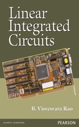
The open-collector outputs of two or more gates can be connected together, as shown in Fig. 11.23(a) and (b). If the outputs of each gate are in ‘HIGH’ state, the final output transistors behave as open switches. The circuit shown in Fig. 11.23(c) is the electrical equivalent circuit for the circuit shown in Fig. 11.23(b).


Fig. 11.23 (a) Open-collector Output of Two and (b) Three TTL Gates Connected Together

Fig. 11.23 (c) Output Transistors of all Gates Work as Open Switches, When Their Outputs are in HIGH State. Electrical Equivalent Circuit for the Circuit shown in (b).
The connection of the open-collector outputs of two and three TTL gates using wired-AND symbol by special AND gate symbol is represented schematically in Fig. 11.24(a) and (b). The concept can be implemented to more number of gates. It shows that the output is HIGH only when all switches are open, that is, only when output of each stage is in HIGH state. Thus, the output is the logical AND operation of the logic function performed by the gates.
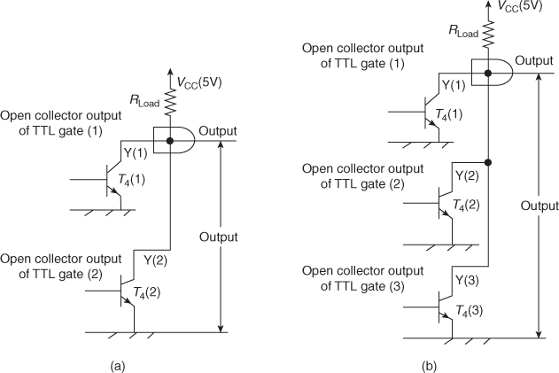
Fig. 11.24 Open-collector Outputs of (a) Two and (b) Three TTL Gates Connected Together Using Wired-AND Gate Symbol
IC 7401 consists of four NAND gates with open-collector outputs is shown in Fig. 11.25(b). The wired output for two NAND gates and its output logic expression is shown in Fig. 11.25(a).

Fig. 11.25 (a) Wire-ANDed Output of Two NAND Gates Showing Their Output Logic and (b) 7401 IC

Fig. 11.26 (a) Wire-ANDed NOR Gates Showing Their Output Logic and (b) IC 7433 Quad NOR Gate
IC 7405 consists of six (HEX) inverter gates with open-collector outputs. For perfect logic operations, pull-up resistors R of value 1 kΩ is used in the circuit, as shown in the figure. The open-collector outputs of three inverters are wire-ANDed with one pull-up resistor ‘R’ as shown in Fig. 11.27(a). From the logic output, the circuit works as ‘three-input NAND gate’. The open-collector gates are slow in their switching because their pull-up resistor has high value (in kilo-Ohm). In this way, long time constants can be obtained, resulting in long propagation delay in switching over between two logic states from ‘0’ to ‘1’ or vice versa.

Fig. 11.27 (a) Three-input NAND Gate Using Wire-ANDed Output of Three Inverters of HEX Inverter IC 7405 with Open-collector Outputs and (b) 7405 IC HEX Inverter
11.7 TRISTATE TTL OUTPUT STAGE
Tristate TTL output stage configuration is a third type of TTL output connectivity available for parallel connection of outputs of various ICs (see Fig. 11.28). The figure shows the parallel connection of logic outputs from multiple ICs. As a result, it increases the number of words in a memory chip.

Fig. 11.28 TTL Inverter Circuit Using Tristate Logic
It utilizes the high-speed operation of the totem-pole arrangement while permitting outputs to be wired-AND (connected together). This TTL inverter circuit implements the tristate logic with following possible output stages: high output impedance, low, and high. As a result, the circuit is called ‘Tristate TTL’. These stages are explained as
- When the output of TTL tristate logic is HIGH, transistor T3 is ON and transistor T4 is in OFF state.
- When the output is LOW, transistor T4 is ON and transistor T3 will be in the OFF state.
- When both transistors T3 and T4 in the totem-pole arrangement are in the OFF state, the output port will be in the ‘high impedance state’. As a result, the output is open or floating, it is neither LOW nor HIGH.
The third condition is an advantageous situation for parallel connection of tristate TTL output stages in memory circuits as in RAM.
Figure 11.28 shows the circuit for ‘tristate TTL logic output stage’. It behaves as an ‘inverter’. Input A is a normal logic input voltage, whereas second input E is an ENABLE input voltage.
- When ENABLE input is HIGH, the circuit works as a normal inverter. When ‘E’ is HIGH, diode D2 is reverse biased and behaves as an open switch. The logic input level of A (0 or 1) determines whether transistor T1 is either ON or OFF.
- When ‘E’ is LOW, diode D2 is forward biased and acts as a closed switch. Regardless of the state of logic input A, both transistors T3 and T4 are in OFF state. Therefore, the output port is at high impedance state. The tristate TTL output stage behaves as tristate inverters for ‘HIGH and LOW input states’ of ENABLE input ‘E’, as shown in Fig. 11.29 with their symbols.

Fig. 11.29 Logic Symbols for Active HIGH ENABLE Input and Active LOW ENABLE Input
Sharing of Data over Common Data Bus Using Tristate Logic Output Stages
Fig. 11.30 shows the common data bus between one input system and two output devices. The distribution of data over the common data bus can be extended to multiple ICs by connecting them in parallel. The switching of data to a particular system is decided by the ENABLE or DISABLE control input voltage levels (1s and 0s), which exist over the chip-select control lines. However, the data bus could be AND-wired among a group of ICs.

Fig. 11.30 Tristate Buffer Used to Control Data Flow Over Common Bus Connecting Multiple Devices in Parallel
11.8 METAL OXIDE SEMICONDUCTOR (MOS) FET SWITCHES IN LOGIC GATES
Based on the principle of fabrication of electronic devices, field-effect transistors (FETs) are of two types: junction field-effect transistors (JFETs) that are used as electronic switches in linear circuits and metal oxide semiconductor (MOS)FETs that are used as electronic switches in digital circuits. MOSFETs are used in logic gates similar to BJTs.
11.8.1 Introduction to MOSFET Switches
The MOSFET works as ON/OFF switch. When MOSFET is not conducting, it has infinite resistance, as no current flows through the transistor. The output voltage is 5 V when the MOSFET is in ON state, as it has almost zero resistance.
These MOSFETs have four types of material structures to obtain different circuit features. They are mostly used in very large-scale integrated (VLSI) circuits. The current flow through the MOSFET is controlled by the electric field; established in the device due to the applied voltage to the controlling Gate terminal. However, the current flow is due to only one type of charge carriers (electrons or holes). Therefore, MOSFET is unipolar device and it has different configurations for various applications. Hence, they are widely used in large-scale integrated (LSI) circuits for applications such as microprocessor, microcontrollers, and memories.
N-Channel MOSFET: Conduction channel between the source and the drain of the MOSFET contains N-type of charges called electrons. It behaves as an electronic switch. For simplicity, the N-channel MOSFET switch is popularly known as NMOS switch. It is further called as NMOS.
P-Channel MOSFET: Conduction channel between the source and the drain of MOSFET contains P-type of charges called holes. It behaves as an electronic switch. For simplicity, this P-channel MOSFET switch is popularly known as PMOS switch. It is further called as PMOS.
Another classification of MOSFETs is done whether the channel for the flow of charge carriers exists before the application of biasing voltages to the MOSFETs or is induced after the application of voltages to the MOSFET devices.
Depletion-mode MOSFET: If the conduction channel between the source and the drain of the MOSFET devices is formed during the device fabrication, it is considered as built-in channel in the device. When the drain supply voltage is given to the device, the drain current flows through the device, even at zero-gate voltage. Then, the device is normally in the conduction or ‘ON’ state. It acts as an ON switch. For the device to be switched OFF, the charges have to be depleted from the channel. Such MOSFET with built-in channel is known as depletion-mode MOSFET.
Enhancement-mode MOSFET
If the channel region between the source and the drain (below the gate region) of the device is empty (without any charge carriers in the channel) and when the drain supply voltage is given to the device, then the drain current is zero as long as the gate voltage is zero. As a result, the device is normally in the ‘OFF’ state and it acts as an OFF switch.

Fig. 11.31 (a) Depletion Mode N-channel MOSFET and (b) Depletion Mode P-channel MOSFET

Fig. 11.31 Enhancement Mode of (c) N-channel MOSFET and (d) P-channel MOSFET

Fig. 11.31 (e) Symbol of NMOS and PMOS transistors
It means that when the input voltage to the gate terminal is ‘0’, the transistor will be in OFF state. Then, the output voltage will be in ‘1’ state. For the device to be brought into conduction state for the MOSFET switch to be ON, a conduction channel is induced (established) between the source and the drain. The induced channel is established by applying positive voltage on the gate for N-channel MOSFET. For P-channel MOSFET, negative voltage is applied to the gate. This method of enhancement of conduction to switch ‘ON’ the device is known as enhancement-mode MOSFET. This means that when the input voltage to the gate terminal is ‘1’, transistor will be in ON state. Then, the output voltage will be in ‘0’ state.
The symbols for the four types of MOSFET switches are shown in the following.
The broken line between the source and the drain of MOSFET device symbol indicates that NMOS (PMOS) devices are of induced channel-type devices. It means that they are enhancement-type devices. They are normally OFF without the gate voltages. When gate voltage of appropriate polarity is applied to MOS transistors, they conduct and turn into ON switches.
Depletion-type MOSFET as a ‘Resistor’
Silicon dioxide material acts as an insulating material between the gate electrode of the MOSFET and both drain and source. If the gate terminal is connected to the bias voltage for permanent conduction of (depletion-type) MOSFET device, then it can be used as a resistor, as shown in Fig. 11.32. The magnitude of the drain current is controlled by the gate voltage.

Fig. 11.32 (a) Connections in a MOSFET as a Resistor (b) Connections in MOSFET as Variable Resistor
Therefore, it acts as voltage-controlled switch. The depletion-type MOSFET is mostly used as a substitute to a ‘resistor’ in VLSI circuits, because MOSFET devices need less area for the IC fabrication.
Enhancement-mode MOSFET operates as a voltage-controlled resistor by varying the gate voltage, as shown in Fig. 11.32.
MOSFET-based digital circuits are classified into three categories:
- NMOS circuits that use only enhanced N-channel MOSFETs have twice the packaging density than the PMOS and also they switch three times faster than the PMOS. NMOS circuits have electrons that are faster moving current carriers whereas PMOS use slower moving holes as their current carriers.
- PMOS circuits that use only enhanced P-channel MOSFETs with holes as current carriers. NMOS and PMOS digital circuits have higher packing density than CMOS circuits, and hence, they are more economical.
- CMOS circuits use both P- and N-channel MOSFETs. Despite the complexity and lower packaging density, CMOS circuits have the advantage of lower dissipation while maintaining a decent high speed.
As a result, NMOS- and CMOS-based digital circuits are most popular. However, the PMOS-based circuits are not considered in the recent designs.
The CMOS gates are being widely used because of the following advantages:
- low power consumption (dissipation) of the gates
- reduction in propagation delay during the output voltage level transitions from ‘0’ to ‘1’ or vice versa
11.8.2 NMOS Inverter, NOR, and NAND Logic Gates
Digital logic gates using NMOSFETs are discussed in the following sections. MOSFETs are used as ON/OFF switches, resistors, diodes, and capacitors.
Inverter Logic Gate Using NMOSFET
Figure 11.33(a) shows the symbol for NOT gate or inverter gate, Fig. 11.33(b) shows the IC pin configuration and Fig. 11.33 shows the truth table of inverter or NOT gate. They are general representations for understanding the concepts of gate operations, irrespective of the nature of active devices and the circuit components in their structures.

Fig. 11.33 (a) NOT Gate (Inverter) Circuit Symbol, (b) HEX Inverter IC Pin Configuration and Truth Table for Inverter (NOT) Logic Gate
NMOS inverter gate consists of enhancement-type NMOSFET (T1) that acts as ON/OFF switch and depletion-type NMOSFET transistor T2 that acts as a resistor and a load resistor. ICs with NMOSFET devices work fast (conduction due to the lightweight charged electrons) and the processing of NMOSFETs is simple. NMOSFETs are widely used in high-speed electronic gadgets such as microcontrollers, memories, and FPGA circuits.
In the circuit of Fig. 11.34(a), when the input voltage to the gate terminal is ‘1’ (HIGH), the enhancement-type NMOSFET (without built-in channel) acts as an ON switch (due to the induced channel between the source and the drain). Then, drain current flows through the resistor and the output voltage will be in ‘0’ (LOW) state. It means that the inverter gate output is ‘0’, when input to the gate is ‘1’.

Fig. 11.34 NMOS Inverter (a) Output is 0 When Input is 1 and (b) Output is 1 When Input is 0
In the circuit given in Fig. 11.34(b), when the input voltage to the gate terminal is ‘0’ (zero), the enhancement-type NMOSFET (without built-in channel) acts as an OFF switch. Then, the drain current through the resistor is zero. The output voltage will be in ‘1’ (HIGH) state.
This means that the inverter gate output is ‘1’, when input to the gate is ‘0’. The input and output voltages are shown in the ‘truth table’ for the inverter gate in Fig. 11.33.
NOR Logic Gate Using NMOSFET
In an NOR logic gate circuit, two NMOSFETs (T1) and (T2) act as ON/OFF switches and NMOSFET (T3) work as a resistor with the drain supply voltage, as shown in Fig. 11.35 (a). The equivalent behaviour of the NOR circuit using mechanical switches S1 and S2 and a resistor is shown in Fig 11.35(b).

Fig. 11.35 (a) NOR Logic Gate Using NMOSFET and (b) Using MOSFET Concept as Switches for NOR Logic Gate and Truth Table for NOR Logic Operation
- If both input A and input B to the MOSFETs are ‘0’, then two transistors T1 and T2 will not conduct. Therefore, they work as open switches and output voltage ‘Y’ of the logic gate corresponds to ‘1’ state.
- If input A = 0, transistor T1 will not conduct and acts as an open switch. At the same time, if input B = 1, transistor T2 will conduct and works as ‘ON’ switch. Then, output voltage ‘Y’ will be ‘0’.
- Similarly, when input voltage A = 1 and input voltage B = 0, output voltage ‘Y’ will be zero.
- For the other combinations, that is, if both input A and input B are ‘1’, the two transistors conduct. Then, they act as closed switches and output voltage ‘Y’ will be zero.
The truth table showing the logic signal operations for NOR gate is shown in Fig. 11.35.
NAND Logic Gate Using NMOSFET
The two-input NAND logic gate with input and output signal operations is given in truth table (see Fig. 11.36). The NAND logic circuit with three NMOSFET transistors (T1, T2, and T3) is shown in Fig. 11.36(a). T1 and T2 are MOSFET switches and T3 is an MOSFET resistor. This circuit can be extended to operate on more number of inputs by simply adding more transistors in series with T1 and T2. The number of additional transistors will be decided by the number of additional inputs.
The NAND logic concept is explained in Fig. 11.36(b) using equivalent switches S1 and S2 with a resistor. The circuit operates on positive logic concepts.

Fig. 11.36 (a) NAND Logic Gate Using NMOSFETs. (b) NAND Gate Working Concept Using Switches S1 and S2 and Resistor Using MOSFET and NAND Gate Operation Using Truth Table
- If both the input voltages A and B are ‘0’ (LOW), two transistors T1 and T2 will not conduct or they are in ‘switched off’ condition. Then, output ‘Y’ will be ‘1’ (HIGH)
- When input A is ‘0’ (LOW), the transistor T1 will not conduct and it acts as an open switch. At the same time, if Input B is ‘1’ (HIGH), transistor T2 will conduct and it will be in ON state. Then, output ‘Y will be in ‘1’ state.
- When input A is ‘1’ (HIGH), transistor T1 will conduct and it acts as a closed switch. At the same time, if input B is ‘0’ (LOW), transistor T2 will not conduct and it will be in OFF state. Then, output ‘Y will be in ‘1’ state.
- If both input voltages A and B are ‘1’ (HIGH), two transistors T1 and T2 will conduct or they are in ‘switched on’ condition. Then, output ‘Y’ will be ‘0’ (LOW).
NMOS and PMOS transistors are used together in a complementary way to form CMOS logic gates. The circuits for CMOS inverter, NAND, and NOR logic gates are discussed in the following section.
11.8.3 CMOS Inverter, NAND, and NOR Gate Circuits
The complementary MOS circuits consist of N-channel MOSFET and P-channel MOSFET on the same substrate. They are interconnected to perform various logic functions such as NOT, OR, NOR, AND, and NAND functions and are required in various applications.
CMOS inverter circuit operation is similar to the other inverter logic gates. The CMOS logic gate circuit has both the gates of the two transistors connected together. Therefore, the gate has common (single) input terminal. NMOSFET and PMOSFETs are connected in series as shown in Fig. 11.37 to form a complementary MOSFET structure. The drain terminals of both P-channel MOSFET and N-channel MOSFET are joined together. The output is taken between the common drain output terminal and the ground terminal. Further, supply voltages to CMOSFET gates are around 5 to 15 V.
NMOSFET operates as a closed or open switch for logic functions whenever its gate is applied with an input voltage of ‘0’ (LOW) or ‘1’ (HIGH), respectively. PMOSFET works as a load resistor to the logic gate to maintain the ON/OFF states.

Fig.11.37 CMOS Inverter Logic Gate
- If input voltage ‘A’ is ‘0’ (LOW), NMOSFET transistor T1 will be in OFF state. Then, PMOSFET will be in ON state and the output voltage is equal to VDD that is ‘1’ (HIGH) state.
- If input voltage ‘A’ is ‘1’ (HIGH), NMOSFET transistor T1 will be in ON state. Then, PMOSFET will be in OFF state and the output voltage is equal to ‘0’ (LOW) state.
From the logic states, the circuit works as inverter or NOT gate.
CMOS NAND Gate Using a Combination of NMOSFET NAND and PMOSFET NOR Logic Gates
Figure 11.38 shows CMOS two-input NAND gate, which is a combination of NOR gate using two PMOSFET transistors (T3 and T4) and NAND gate using two NMOSFET transistors (T1 and T2). If the input voltages are input A and input B, output Y = (A·B)′.
The NOR gate consists of two P-channel MOSFETs (T3 and T4) and they are connected in parallel. The NAND gate uses two N-channel MOSFET transistors (T1 and T2) and are connected in series. (Driver transistors are series-connected.) The circuit layout is shown in Fig. 11.38.
The two input terminals A of the transistors T2 and T3 are connected together to function as a single input A. The two input terminals B of the transistors T1 and T4 are connected together to function as a single input B. Then, the complete CMOS NAND gate has two-input logic terminals A and B and one-output terminal, as shown in Fig. 11.38.

Fig. 11.38 CMOS NAND Logic Gate Using a Combination of NMOS NAND and PMOS NOR Gates
When the gate voltage is negative with respect to its source, a P-channel MOSFET is ON. The opposite is true for N-channel MOSFET, that is the gate voltage needs to be positive (with respect to its source) to turn the N-channel MOSFET to be ON.
Truth Table of Two-input NAND Gate Using CMOSFET Devices (ON/OFF States of MOSFET Transistor Switches T1, T2, T3, and T4)

The specifications of CMOSFET logic gate supplied by manufacturers will be similar to that of the BJT logic Gates.
Specifications for Various Logic Gates
- Input and voltage levels to satisfy the ‘1’ and ‘0’ level operations at input and output ports of logic circuits. The type of voltage and current magnitudes depend upon the positive or negative logic. Normal logic is positive logic.
- Power consumption in ICs depends upon active devices in the circuits (power dissipation magnitudes range from about 50 nW to few tens of microwatts).
- Propagation delays for voltage transitions between ‘1’ and ‘0’ states and vice versa. (Typical propagation delays are of the order of 20–30 ns) (transition times are of the order of 20–60 ns).
- Fall and rise times of responses (typical values of rise and fall times is below 20 ns).
- Operating speeds of the order of 20 to 100 ns.
- Range of supply voltages (5 V to 15 V).
- Noise immunity.
- Fan-in and fan-out capabilities in the interfacing of various circuits.
- Operating temperatures.
The differences in specifications are due to the advances in material processes and fabrication technologies associated with VLSI circuit innovations.
Three-input NAND Gate Using CMOSFETs
Three-input NAND gate using CMOSFETs with relevant inputs of CMOS pairs for input A, input B, and input C tied together is shown in Fig. 11.39.

Fig. 11.39 Three-input NAND Gate Using CMOSFETs
CMOSFET NOR Logic Gate Using NMOS NOR Gate and PMOS NAND Gates
Figure 11.39 shows a two-input CMOS NOR gate. Here, T1 and T2 (both P-channel MOSFETs) are connected in series and T3 and T4 (both N-channel MOSFETs) are connected in parallel. This circuit functions like an NAND circuit, when a low input signal turns the output ON and vice versa. The following truth table is given to understand the logic operations of a two-input NOR Gate. Figure 11.39 shows the CMOS NOR gate with inputs A and B tied together.
Truth Table for NOR Gate Using CMOSFET Devices (ON/OFF States of MOSFET Transistor Switches T1, T2, T3, T4)

CMOS NAND (using N-channel) and NOR (using P-channel) gates do not have identical output performance, as P-channel transistor has greater ON resistance than N-channel transistor; this is similar to the case when similar transistors are connected in series. For the same number of inputs, a multi-input NAND gate is generally faster than multi-input NOR gate.
11.8.4 Advantages and Disadvantages of CMOS Family

11.8.5 CMOSFET IC Series Characteristics
CMOS ICs have better performance characteristics when compared to TTL circuits. Therefore, CMOS ICs are predominantly used in latest applications. CMOS logic circuits have special functional ICs in addition to already existing TTL functional circuits.
Pin Compatibility: If the pin configurations of CMOS ICs and TTL ICs are same, ICs of both technologies are pin compatible.
Identical Functionality: If the logic functions of both CMOS ICs and TTL ICs are identical, they do equivalent functions.
Operating Speed: CMOS ICs are slower than TTL series by approximately 25 to 100 ns. Operating speeds vary for circuits with the sub-family of CMOS. 4000 series of CMOS circuits were originally from RCA and 14000 series of CMOS circuits are later developed by Motorola companies. Both the series work with low power dissipation and operate on voltages ranging from 3 to 15 V. They are slower in speed when compared to TTL circuits.
Simpler Fabrication Process: Fabrication process of CMOSFET is simpler than TTL systems and packing density is more. More number of CMOS circuits can be assembled in Silicon Wafers of desired area when compared to TTL circuits. Therefore, the circuit cost also becomes low.
Fan-out: Fan-out for CMOS depends on the permissible maximum propagation delay. Typically, CMOS outputs are limited to a fan-out of 50 for low frequency operation (1 mHz). Fan-out capability decreases for high frequency signals.
Power dissipation (PD): Power dissipation in a logic gate is the product of power supply voltage VCC and current IC during the circuit operation. Power dissipation PD = (VCC × IC). Applied voltage VCC is constant, whereas the magnitude of current drawn from the supply voltage depends upon the nature of logic states ‘1’and ‘0’. Thus, the power dissipation is simply a function of the different dynamic states of logic gates. Under the DC condition, CMOS IC has low power dissipation and that increases in proportion with the frequency of circuit switching (how fast the logic states change). For example, an NAND gate with supply voltages ranging from 5 V to 15 V have a PD from 0.001 mW to 0.01 mW. Typical value of VDD is 5 V. At a frequency of 100 kHz, PD is of the order of 0.1 mW and it increases to 1 mW when the frequency increases to 1 mHz.
Unused Inputs: Similar to any unused logic gates on a chip, CMOS inputs should always be connected – to some input – to a fixed voltage (0 V or VDD) or another input. This is a common rule for all logic gates and it is always necessary to provide a valid input signal to the input terminal. If not, the CMOS circuit can be subjected to slightest signal noise, increasing power dissipation and even heating the device.
For any unused inputs, AND and NAND gates should connect to default logic 1, and OR and NOR gates to default logic 0. Figure 11.39 shows an unused input tied to another input.
POINTS TO REMEMBER
- AND Logic Operation: For two-input AND gate, output Y is TRUE (1) if and only if both the inputs, input A is TRUE (1) and input B is also TRUE (1). It has two or more inputs and single output.
- OR Logic Operation: For two-input OR gate, output Y is TRUE (1) if input A is TRUE (1) or input B is TRUE (1) or if both input A and input B are TRUE (1). Boolean expression: Y = (A + B). It can be extended to any number of inputs. It can operate on multiple inputs and produce a single output.
- NOT/Inverter Logic Operation: Output voltage levels of NOT/inverter gate represent inversion or complement operation to input signals. NOT circuit inverts an input signal. At the same time, binary signal levels and the wave shapes of voltages do not undergo any changes during transmission through gates. The inverter circuit operates on two-input voltages V(0)/V(1) (signals are shown in Fig. 11.3(a)).
- When the input voltage is V(0) that is ‘0’ state, then the output voltage will be V(1) that is ‘1’ state.
- When the input voltage is V(1) that is ‘1’ state, then the output voltage will be V(0) that is ‘0’ state.
- NAND Gate: NAND Operation: It is a combination of NOT and AND operations in a single module of AND and NOT circuit operations.
SUMMARY
An integrated circuit is also known as IC, microcircuit, microchip, silicon chip, or chip. It is a miniaturized electronic circuit consisting of semiconductor devices and passive components. Integrated circuit is a complex electronic structure in which multiple electronic components are embedded into a small package. Transistors, diodes, resistors, and capacitors can be integrated into an IC in large quantities, up to tens of millions of devices in Microprocessors and Programmable Logic Arrays.
- The different characteristics of the logic family are propagation time delay, fan-in and fan-out, noise margin, noise immunity and power dissipation.
- Propagation time delay is the average transition delay time for the signal to propagate from input to output when the signal charges its value. This determines how fast the logic system can operate.
- Fan-in: The maximum number of inputs that can be applied to a logic gate is known as fan-in.
- Fan-out: The number of gates that can be driven by logic gate.
- Noise margin is the property of logic circuit to withstand unwanted noise voltage at input or the maximum value of noise signal that a system can reject with performance unaffected.
- Noise Immunity: The ability of the circuit to tolerate noise signal is called as noise immunity of the circuit.
- Power Dissipation: The power consumed by the gate that must be available from the power supply.
- Transistor–transistor logic is the most popular amongst all logic families because of its speed, good fan-in, and fan-out. This switch uses a multiple-emitter transistor that can be easily fabricated.
- A totem-pole connection has a major advantage that it offers the same low output impedance in both output states (HIGH and LOW ). Tristate gate utilize the high-speed operation of the totem-pole arrangement, when input enabled.
- Transistor–transistor logic requires a good power supply; further, it is used when the speed is considered to be very important.
- 11. CMOS 4000 is good for battery equipment, in which the speed is not so important.
QUESTIONS FOR PRACTICE
- Explain the working of logic gates inverter circuits using TTL and CMOSFETs.
- Explain the working of logic gates AND circuits using TTL and NMOSFETs.
- Explain the working of logic gates NAND circuits using TTL and NMOSFETs.
- Explain the working of logic gates OR circuits using TTL and NMOSFETs.
- Explain the working of logic gates NOR circuits using TTL and NMOSFETs.
- What is meant by tristate logic?
- Draw the circuit of tristate TTL logic and explain its functions.
- Explain totem-pole TTL gate with suitable circuit diagrams.
- Write short notes on TTL gates.
- Explain the operation of NMOSFET as switch and resistor to act as load.
- List out the advantages of CMOS logic.
- Draw the circuit of CMOS NOT gate and verify the Boolean function.
- Draw the circuit of CMOS AND gate and verify the Boolean function.
- Compare different logic families and mention their advantages and disadvantages.
- Draw the schematic circuits of CMOS NAND and CMOS NOR gates and explain their functions with the help of truth table.
- What are the advantages and disadvantages of CMOS over TTL gate?
- 17. Compare the relative merits of NMOS, CMOS, TTL, and ECL logic families.
MULTIPLE-CHOICE QUESTIONS
- CMOS inverter circuit consists of the following two types of MOSFETs:
- N-channel D-MOSFET and P-channel E-MOSFET
- N-channel D-MOSFET and N-channel E-MOSFET
- N-channel E-MOSFET and P-channel MOSFET
- N-channel E-MOSFET and N-channel E-MOSFET
[Ans. (c)]
- The logic family which has minimum power dissipation feature is
- ECL
- CMOS
- I2 L
- TTL
[Ans. (d)]
- TTL logic family gates have the following output circuit features
- Totem-Pole output
- Open-collector output
- Tristate output
- All the above
[Ans. (d)]
- Processing of MOS ICs is less expensive than bipolar ICs primarily because
- Their diffusion processes are less
- Their high packing density
- They need no component isolation
- They have less number of components
[Ans. (b)]
- Main advantage of using totem-pole output stage in standard TTL logic family is
- Increase in the output impedance
- Decrease the switching delay between HIGH and LOW output states
- Facilitate a wired-AND logic connection
- Increase in the noise margin
[Ans. (b)]
- For standard TTL, the logic 0 has a voltage level between
- 0 and 1 V
- 0 and 0.8 V
- 0 and 0.5 V
- 0 and 0.4 V
[Ans. (a)]
- TTL systems operate on high and low voltage levels to represent 1s and 0s.
- +5 and −5 V
- +5 and 0 V
- +15 and −15 V
- +25 and −25 V
[Ans. (b)]
- In standard TTL, the ‘totem-pole’ output stage has the following main advantage
- Reduction in propagation delay between output states
- Multiple-emitter transistor input stage
- Power dissipation minimization
- Increase in speed of operation
[Ans. (d)]
- Main advantage of TTL circuits with active pull-up transistor is
- Increase in operation speed and decrease in power dissipation
- Wired-AND operation
- Common bus operated system
- Suitable for IC fabrication
[Ans. (a)]
- Typical power dissipation of MOS inverter is of the order of
- 100 mW
- 10 nW
- 100 nW
- 10 mW
[Ans. (b)]