10
Analog to Digital and Digital to Analog Data Converters
Objectives
To understand the theory, analysis, and design concepts of data converters
- Data in the real world is in the form of analog signals. For example, temperature, pressure, biopotentials from human body, and so on can be detected by using appropriate sensors (transducers). Though the sensed quantities are analog signals, they can be converted into digital signals for measurement and practical applications. Electronic circuits used for analog to digital signal conversion are called analog to digital converters (ADCs). The basic principles of analog to digital signal conversion using different techniques are explained.
- Electronic circuits in devices such as compact disc (CD) player and video player circuits use digital to analog converters (DACs). For example, the final loads are the loud speakers for audio signals. They operate only on analog quantities. Hence, DAC circuits are explained. On similar lines, digital to analog signal conversion techniques using various circuits are explained.
10.1 INTRODUCTION
In long-distance telephone calls, the microphone housed in a telephone is used to convert speech into electronic (analog) signals. They are converted to digital data using ADCs. This digital data is transmitted for distance transmission using computers and digital exchanges (CDOT exchange). Signals from the digital exchanges are transformed back to analog signals by using DAC circuits. The received analog signal is converted back to speech by the loudspeakers (transducers) in the telephones (telephone handset, mobile phone, i-phone etc.).
Physical system variables can be measured using a signal transducer. For example, the transducers in an electrocardiogram (ECG) convert the biopotentials of the body into electrical signals of small magnitude. The measured signal will be analog in nature. As the possibility of getting reliable and accurate measurements is high with digital technology, the measured analog signal will be converted to a digital signal format by an analog to digital converter (ADC) circuit using an operational amplifier (op amp) such as μ A 741 or μ A 1458 (dual op amp).
The digital output of the ADC is then processed in the database and other logic systems depending upon the application. It is then converted into analog signals using a digital to analog converter (DAC) circuit. The final analog electrical output is applied to an electrical control circuit for practical application. In one form of DAC, a summing amplifier using an op amp and a ladder network (consisting of R-2R elements) converts binary or digital signals into analog signals.
10.2 Analog TO DIGITAL DATA CONVERTERS
10.2.1 Analog Switches
An analog switch is also called a bilateral switch. It functions as a relay unit. In electronic circuits, (a) bipolar junction transistor (BJT), (b) field-effect transistor (FET), (c) metal oxide semiconductor FET (MOSFET), and (d) complementary metal oxide semiconductor (CMOS) devices are used as a replacement to mechanical switches. Transistors operate in the closed or open condition between two points in a circuit. Such conditions are obtained by using a control signal for operation as a switch. For example, P-channel MOSFETs are used as electronic switches in transistor−transistor logic (TTL) circuits.
- Electronic switches are available in the form of integrated circuits (ICs). They are available as single pole single throw (SPST) and double pole double throw (DPDT) switches.
- The combination of P-channel MOSFET and N-channel MOSFET devices functions as electronic switches. When the electronic switch is ON, analog and digital signals can conduct in both directions. When the switch is in the OFF condition, the circuits on either side of the switch are isolated. The control signal and the input/output signals are isolated.
- They have applications as audio, video signal routing, and data switches. Other applications are in multiplexers and demultiplexers.
Circuit: For a P-channel MOSFET device, the gate is of an N-type material and the channel is of a P-type material. The biasing voltage VDD and control signal VGS are shown in Fig. 10.1.

Fig. 10.1 P-channel MOSFET as Electronic Switch
- MOSFET works as a switch in the ON condition if zero voltage (logical 0 state) is applied to the gate terminal. It works as a closed switch with resistance less than 100 ohms.
- When logical 1 state with a positive voltage is applied to the gate, MOSFET works as an open switch with very high resistance.
Thus, the control signal obtained from the logic level voltages or other similar control signals can control and operate the P-channel MOSFET as a switch.
10.2.2 Analog to Digital Data Conversion
- An ADC circuit converts a continuous signal into a digital signal using the sampling process. One simple technique uses sample and hold circuits consisting of an op amp and FET switches. A digital signal assumes discrete outputs at definite time intervals.
- The output of an ADC consists of digital values representing the binary values of 0s and 1s in digital form. The number of discrete values depends upon the resolution of the ADC and the method of reconstruction (recovery) process used by the DAC to get back the original analog signal. The number of discrete levels sampled is represented as 2N, where N represents the number of samples.
- Temperature, pressure, and other such data in nature are in the form of analog signals (continuously varying signals). For practical use in real-time applications, these analog signals need to be converted into electrical analog signals by using different types of sensors (transducers). When analog signals are used in digital instruments and industrial process control instrumentation, they are converted into digital format using ADC ICs. Digital signal conditioning and processing is done using microcontrollers. Such processes provide noise-free, accurate systems as in energy monitoring and management systems.
Advantages of Digital Systems
- 1. Digital signals can be processed and updated easily by using software programs. Several types of ADCs are available in IC form.
- Digital signal processing provides noise immunity.
- They have storage capability in various forms such as DVDs, audio CDs, random access memory (RAM), read-only memory (ROM), cloud computing, and emails.
- There is flexibility.
- Lower computer processing power has made analog to digital conversion more popular. Today, telecommunications industry mostly uses digital communications, for example, television, long-distance telephone, and video using Skype on computer systems.
Disadvantages of Digital Systems
- The cost for the implementation of even a small system is high in the digital domain.
- During the process of converting analog to digital signals, sampling and quantization results in quantization errors, which in turn results in loss of information.
- They operate satisfactorily with low-frequency signals only.
Advantages of Analog Systems
- Analog systems work at a higher speed than digital systems.
- They can work with high-frequency signals.
- Signals in the real world are of analog nature.
Basic Block Diagram to Illustrate the Concept of Analog to Digital Data Conversion
When an analog input signal is applied to an ADC, it produces digital output signals in the binary form of 0s and 1s. The voltage levels of the binary signals depend upon the type of hardware used in the logic circuits. The binary output signals can be assumed as samples of data at different instants of time sequence such as D1, D2, D3, ..., Dn. Figure 10.2 shows the block diagram of an ADC.

Fig. 10.2 Block Diagram of an Analog to Digital Signal Converter
10.2.3 Different Types of Analog to Digital Converter Circuits
Analog to digital converter circuits are of two categories:
- Direct type ADCs:
- Parallel comparator (flash) ADC
- Counter type ADC
- Successive approximation (SA) ADC
- Integrating type ADCs:
- Single slope type ADC
- Dual slope type ADC
These ADCs are discussed in detail in the following sections.
10.3 PARALLEL COMPARATOR (FLASH) TYPE Analog TO DIGITAL CONVERTER
The following are some of the salient features of the flash type ADC:
- Simple structure
- Fast conversion (hence the name flash ADC)
- High cost
- Possibility to improve resolution by increasing the number of comparators
- High accuracy
A flash ADC consists of the following components:
- Analog input signal (for conversion to digital signal)
- Linear voltage divider network consisting of resistors (capacitors in IC form are used for linear division of the analog input signal)
- Set of eight op amp parallel comparators (driven by a resistive voltage dividing network and the output voltages fed to the encoder)
- Encoder (converts the inputs from the comparators into binary outputs fed to digital display)
- Binary (digital) outputs
- Digital display (seven-segment display)
The circuit of a flash type ADC is shown in Fig. 10.3.

Fig. 10.3 Flash Type Analog to Digital Converter
The maximum frequency fmax of a sine wave that can be digitized is expressed by the equation
![]() Hz
Hz
where
n = number of bits used for conversion
TC = conversion time to undergo analog to digital conversion process.
Principle of Operation
- One input of each op amp comparator is connected to an analog input voltage Vin.
- The second input terminal of the comparators is connected to a part of reference voltage Vref obtained from linear voltage division using resistors (capacitors in the IC form).
- The available voltage levels at each node (connected to the comparator input terminals) of the resistor chain are equally divided between reference voltage VR and ground. The voltage levels at each node of the resistor chain starting from the ground terminal are as given in Table 10.1.
Table 10.1 Nodal Voltages in Resistor Chain Used in Flash Type Analog to Digital Converters

- The role of the op amp comparators is to compare the input signal voltage and reference voltage at each node of the comparator and generate a digital logic output (analog to digital conversion) as follows (refer Table 10.2):
Table 10.2 Digital Logic Output Corresponding to Input Signal and Reference Voltages

- The comparator produces logical 1 (one) output if the input signal for the ADC is larger than the reference voltage level from the resistor chain.
- The comparator produces logical 0 (zero) output if the input signal for the ADC is less than the reference voltage level from the resistor chain.
- If the voltage of the analog input signal is equal to the node voltage from the resistor chain, the comparator output produces the binary state corresponding to its previous output state.
- Binary output voltages from the eight parallel comparators are fed to an encoder circuit input port. They can be considered as B0, B1, B2, B3, B4, B5, B6, and B7.
- An 8-bit to 3-bit encoder circuit is considered here. The encoder output voltages form the binary code with digits D0, D1, and D2.
The output pattern of states (logical 0s and 1s) of the parallel comparators and the binary code corresponding to the analog input signal to the flash type ADC are given in Table 10.3.
Table 10.3 Conversion of Analog Signal Voltage Levels to Binary Levels

The conversion of analog signal voltage levels to binary levels occurs simultaneously due to parallel conversion by the comparator circuits. Hence, analog to digital data conversion is faster in flash type ADCs.
Disadvantage
The number of required comparators doubles for every added bit requirement as follows:
A 2-bit ADC needs (2N − 1) = (22 − 1) = 3 comparators.
A 3-bit ADC needs (2N − 1) = (23 − 1) = 7 comparators.
A 4-bit ADC needs (2N − 1) = (24 − 1) = 15 comparators.
Hence, a disadvantage of flash type ADCs is that they need more comparators.
Applications
ADC outputs are used in the following applications:
- Digital displays
- Video signal recording
- Radio frequency signal processing where conversion times are less than 100 μC
Example 10.1
For a sinusoidal signal of frequency 100 Hz, calculate the required conversion time TC for the conversion of the signal into 4-bit digital data.
Solution: ![]()
Therefore, conversion time ![]()
Example 10.2
Calculate the voltage at node 4 for a flash ADC having eight comparators and eight resistors of equal value R as shown in Fig. 10.3. Reference voltage VR = 16 V.
Solution: Voltage at node 4: ![]()
10.4 COUNTER OR TRACKING TYPE Analog TO DIGITAL CONVERTER
Counter type ADC is one of the simplest ADCs. The following are the components of counter type ADCs:
- Analog input signal (for conversion to digital signal)
- Op amp comparator
- AND gate
- Clock generator
- DAC
- Reference voltage
- Binary counter
- Digital output
- Digital display
The schematic block diagram of a counter type ADC is shown in Fig. 10.4. Its input is an analog signal and output is a digital signal, which is a collection of 0s and 1s.

Fig. 10.4 Counter Type Analog to Digital Converter
Principle of Operation
- Reset the binary counter to zero (before starting the analog to digital conversion).
- At the beginning of the ADC process, voltage VDAC (VD) = 0.
- There are two input signals to the op amp comparator.
- The input signal of the ADC is connected to the input terminal of the comparator.
- The output voltage VDAC of the DAC is compared with the analog input signal of the ADC.
- The input signals to the AND gate are the output voltage from the comparator and the clock generator output (clock pulses).
- If the analog input signal Vin is greater than 0, its comparator output will be logical 1. The logical 1 output enables the AND gate for transmission of clock pulses to the binary counter. The counter then receives the clock pulses.
- The clock pulses from the AND gate are connected to the binary counter.
- The binary counter output is the digital output. It will become 0001.
- The maximum number of count levels N = 2n, where n is the number of bits in the counter.
- The digital output from the binary counter is converted to analog voltage VDAC/1by the DAC and produces an output voltage VDAC = 1. If the analog signal is greater than one at this instant of time, the comparator output goes to logical 1. It enables the AND gate, and the counter advances and reads 0010. The output of the DAC is continuously compared with the analog input (to ADC) for conversion into digital output display.
- The comparison of the analog signals Vin and VDAC (output of DAC) is made by the comparator. If its output is greater than one, counting progresses. When the analog input signal equals or is less than the DAC output, the counter stops. The digital output is used for the external process.
- 13. The binary counter output is the digital output, which is the converted signal of the external analog input signal. Thus, analog to digital signal conversion takes place. The digital output is displayed in the seven-segment display.
Thus, the following are the basic operations involved in the working of a counter type ADC:
- Reset and start counter.
- The DAC converts the digital output of the counter to the analog voltage VDAC.
- The analog input signal voltages Vin and VDAC are compared by the comparator.
- If the comparator produces logical 1 output voltage, it operates the counter.
- The output of the counter is the digital output of the analog voltage used for the conversion.
- The cycle of events during the ADC conversion process repeat.
- When the analog input signal equals or is less than the DAC output, the counter stops.
Advantages
- The operation is simple and straightforward.
- Computer data acquisition systems.
Disadvantages
- The variable conversion time depends upon the amplitude of the analog signal.
- The speed of conversion is low because of the following reasons:
- Time taken in the conversion of the binary input into analog output by the DAC
- Limitation in the response of the comparator in the comparison process between the external analog input signal and the input from the DAC
- The time taken for conversion by the DAC will be high for large signals.
Example 10.3
Calculate (a) the conversion time for one cycle of the analog to digital conversion process and (b) the percentage resolution R of the ADC when it uses a 4-bit counter and the clock pulses operate at a frequency of 2.5 MHZ.
Solution:
- Number of output levels N of a 4-bit counter = 2n = 24 = 16 levels
Counter time period T =

Total counting time interval = T × N = 0.4 × 10−6 × 16 = 6.4 μs
- Percentage resolution R =
 = 6.25%
10.5 SUCCESSIVE APPROXIMATION TYPE Analog TO DIGITAL CONVERTER
The SA ADC converts analog signal waveform into digital signals. The various components of an SA ADC are as follows:
- Analog input signal
- Output voltage VDAC from the DAC for comparison by the comparator circuit
- Analog voltage comparator
- Reference voltage Vref to normalize the input
- Successive approximation register (SAR) consisting of (a) logic block, (b) clock generator, (c) shift register, and (d) storage register
- DAC circuit
- Clock generator
- Digital output from SAR
The SA ADC consists of two additional circuits—shift register and logic circuits—than the counter type ADC. The transition diagram for an SA ADC for a 3-bit operation is shown in Fig. 10.5.

Fig. 10.5 Successive Approximation Type Analog to Digital Converter
Principle of Operation
- The conversion process is initiated when a start pulse (SOC) is applied to the SA ADC. The start pulse makes transitions on the shift and storage registers with their most significant bit (MSB) set to 1 and the binary word (output) will be 100 in the seven- segment display.
- Initially, during the first approximation, the output voltage VD of the DAC is set to half the full-scale voltage VFS. If the full-scale voltage is 20 V, VD is set at 10 V.
- The SAR takes the input from the output of the comparator and provides an approximate digital output (code) of the applied input signal to the DAC. The DAC produces an output voltage proportional to the binary data output obtained from the SAR.
- Now, there will be two input voltages to the comparator: (a) analog input signal voltage VA and (b) feedback voltage VD from the DAC outputs.
- If the analog voltage VA is greater than VD, the binary output of the SAR will retain 1 at its MSB and the SAR displays 100.
- If the analog voltage VA is less than VD, the binary output of the SAR will reset 1 to 0 at its MSB and pushes 1 to the next lower position. Then, the SAR displays 010. The DAC converts this binary word 010 to the corresponding analog voltage, say
 .
. - As long as the input voltage lies between 10 and
 12.5 V, the SAR has an output of 100. The DAC produces the corresponding voltage, say
  . It is fed to the comparator input for successive comparison with the external input signals.
  and the new input signal are now compared.
- As long as the input voltage lies between 12.5 and
 15 V, the SAR has an output of 101. The DAC produces the corresponding output voltage, say
  .
.  and the new input signal are now compared.
 - If the input voltage lies between 15 and
 , the SAR has an output of 110. The DAC produces the corresponding voltage, say
  .
.  and the new input signal are compared.
 - 11. If the input voltage lies between 17.5 and (Vmax = 20) 20 V, the SAR has an output of 111. The DAC produces the corresponding voltage
 . Similar levels of input signal voltages and comparison with their corresponding DAC feedback voltages can be explained from Fig. 10.6. The digital outputs are also shown in Figs 10.5 and 10.6.

Fig. 10.6 Input Signal expressed as a Fraction of Full Scale Voltage
The working environment is similar irrespective of the number of bits in the conversion process of analog to digital domain. For an SA type ADC, the time for digital to analog signal conversion
![]()
where
n = number of bits of digital output
f = clock frequency
Example 10.4
Calculate the conversion time TSA DAC for an SA type ADC with 12-bit output to the counter and working with a clock frequency of 3 MHz.
Solution: Time ![]()
n = number of bits = 12 and clock frequency f = 3 MHz
![]()
Example 10.5
Calculate the conversion time TSA ADC for an SA Type ADC with 10-bit output to the counter and working with a clock frequency of 5 MHz.
Solution: Time ![]()
n = number of bits = 10 and clock frequency f = 5 MHz
![]()
Advantages
- Less time for analog to digital signal conversion
- High resolution
- Less circuit cost, when compared to the other ADC types
Disadvantage
It is slower than the other types of ADCs.
10.6 SINGLE SLOPE TYPE Analog TO DIGITAL CONVERTER
Single slope ADC is a type of integrating ADC. The following are the various features in a single slope analog to digital signal converter (Fig. 10.7):

Fig. 10.7 Single Slope Type Analog to Digital Signal Converter
- An analog signal Vin is provided as the input for conversion to digital signal.
- A linear ramp voltage is produced by an op amp ramp generator (whenever triggered by a reset signal).
- The op amp comparator is applied with (a) an analog signal and (b) a linear ramp signal. Whenever the ramp voltage equals the magnitude of the analog signal, the voltage of the comparator output becomes high.
- The AND gate has two input voltages: (a) timing control voltage and (b) clock pulses of uniform amplitude and stable frequency.
- The linear ramp voltage is used to convert the unknown analog input signal into a proportionate time interval. It is done by the timing signal and the AND gate.
- Clock pulses are allowed to enter the binary counter whenever the comparator output is a high voltage. Otherwise, the clock pulses are stopped (disconnected) and do not reach the binary counter.
- The AND gate allows the clock pulses to enter the binary counter or stops them depending upon the level of output voltage of the comparator (explained in point 6).
- 8.The timing and control circuit provides the control signal to the AND gate to allow the clock pulses to enter the binary counter or to stop them. The clock pulses are counted by the binary counter during the latch operation done according to the time interval (proportional to the analog input voltage).
- The encoder provides the digital display proportional to the measured input voltage.
Principle of Operation
OP Amp Comparator. The op amp comparator is applied with two signals: (a) analog signal to positive input terminal Vin and (b) output signal from ramp generator Vramp to negative input terminal. The comparator compares the two input signals. When the ramp voltage equals the analog signal, the comparator output becomes high.
AND Gate. The comparator output and a set of clock pulses (two signals) of uniform amplitude and stable frequency are applied to the AND gate. The AND gate passes the clock pulses to the binary counter whenever the comparator output is a high voltage. Otherwise, the clock pulses are stopped (disconnected) from entering the binary counter. The pulses are counted and displayed in the digital display.
Ramp Generator. The high output of the comparator triggers the ramp generator (through a control switch) to produce the ramp signal. The ramp voltage Vramp is connected to the inverting (−) input terminal of the comparator. When the ramp voltage goes sufficiently positive and exceeds the input signal, the comparator output turns into a low voltage. The low output voltage from the comparator triggers the AND gate and stops the entry of clock pulses into the binary counter.
Control Circuit and Binary Counter. The control circuit latches the digital data and displays it in the counter. The digital output can be made available as a digital signal proportional to the analog input.
Application
The principle of the single slope type ADC was initially used in digital voltmeters (DVMs).
10.7 DUAL SLOPE TYPE Analog TO DIGITAL CONVERTER
The dual slope ADC is another type of integrating converter. The schematic diagram of a dual slope ADC is shown in Fig. 10.8. It is also known as a dual ramp converter circuit. It is used for the measurement of analog signals (voltages) using digital techniques in DVMs. The digital measurement shows the measured alternating current (AC) or direct current (DC) voltage as numbers in the display unit. Thus, the measurement of analog signals is easy to read and reliable. Sample and hold circuits are not used for analog to digital conversion in dual slope ADCs.

Fig. 10.8 Dual Slope Type Analog to Digital Converter Circuit
The dual slope ADC in a DVM consists of the following:
- The electronic single pole double throw (SPDT) switch connects either the analog input (data) signal or the reference voltage (−Vref) to the op amp integrator at appropriate times.
- If positive voltage is to be digitized, the reference voltage is negative (−Vref). If negative voltage is to be digitized, the reference voltage is positive (+Vref).
- The buffer amplifier maintains high input impedance at the input port of the measuring instrument so that it will not load the source or drain power from the source.
- The op amp integrator circuit is a ramp voltage generator using the principle of capacitor charging to the analog input signal amplitude V1 for a time interval T fixed by the counter. The integrator circuit output increases linearly like a ramp voltage, as shown in Fig. 10.8.
- The op amp comparator circuit has two input voltages:
- Output voltage of the integrator circuit connected to the comparator input circuit
- Reference voltage VR
The comparator circuit gives a stop command whenever its output voltage exceeds the reference voltage VR. It is kept at 0 volts in this circuit.
- The control logic circuit controls the clock, starts the count, and clears the count pulses of the counter circuit and the switching actions of the two switches.
- An N-stage binary counter and register is also available.
- The clock generator could be a simple AND circuit. It has two inputs:
- Output voltage of comparator circuit
- Clock generator output
The clock generator output is connected to a control logic circuit.
- The seven-segment display for digital output voltages displays the magnitude of the measured voltage as a numerical value (number).
Principle of Operation
When the DVM start signal is switched ON, the following operations are initiated:
- The SPDT switch-1 connects the input voltage Vin (for measurement) to the integrator circuit through the buffer amplifier.
- Switch-2 across the capacitor in the integrator circuit becomes open to allow the capacitor to charge from the initial zero voltage (VC = 0) to the applied input voltage.
- The digital counter is initially reset to zero.
The input voltage drives a current i through the resistor R and capacitor C in the integrator circuit. Then the capacitor charges to a voltage ![]() . The capacitor voltage VC(T1) is the integrator output voltage at time T1 as shown in Fig. 10.9. It is a linear ramp voltage if the input voltage is DC. It is a negative voltage, as seen by the integrator voltage expression, when the input voltage is positive. The integrator output voltage
. The capacitor voltage VC(T1) is the integrator output voltage at time T1 as shown in Fig. 10.9. It is a linear ramp voltage if the input voltage is DC. It is a negative voltage, as seen by the integrator voltage expression, when the input voltage is positive. The integrator output voltage ![]() is applied to one of the input terminals of the op amp comparator.
is applied to one of the input terminals of the op amp comparator.

Fig. 10.9 Integrator Output Voltages of a Dual Slope Analog to Digital Converter
The reference voltage VR to the comparator circuit is kept zero by grounding that terminal on the comparator. Then, the comparator output voltage will become high and will operate the control logic circuit. The counter counts the clock pulses C1 during the interval zero to T1. At the end of period T1, the integrator circuit integrates the total input voltage (when the capacitor is totally charged to the input voltage).
Then, the SPDT switch-1 is connected to the voltage −Vref by the control logic circuit. Now, the input voltage to the integrator circuit is the constant reference voltage (−Vref). The capacitor voltage discharges from the negative voltage ![]() and rises to zero at time T2. At this time T2, the count in the counter can be considered as C2.
and rises to zero at time T2. At this time T2, the count in the counter can be considered as C2.
The comparator output voltage becomes low and changes the previous actions in the control logic circuit. The following actions are taken up by the control logic circuit now:
- Clock pulses are stopped from entering the counter and the counter stops the pulse count.
- Switch-2 gets closed and the capacitor voltage remains at zero.
The measurement of the voltage Vin can be calculated from the known values of Vref, T1, and T2. Input voltage  .
.
The time intervals T1 and T2 are known in terms of the digital count CT = (C1 + C2), where (a) C1 is the digital count at time T1, (b) C2 is the count at T2, and (c) CT is the total digital count during the period zero to T2.
The input voltage Vin can be expressed in terms of the final digital count CT observed in the counter: ![]() , where N is the number of bits representing the digital display and count = 2N.
, where N is the number of bits representing the digital display and count = 2N.
The integrator circuit output voltages appear as sawtooth voltage in the inverted plane, as shown in the waveforms of Fig. 10.9.
If the input voltage to the ADC (integrator) is negative, then the ramp will be positive going, and positive reference voltage has to be used for discharging the capacitor. The sawtooth pattern of the integrator output will be in normal view.
From Fig. 10.10, it is understood that ![]() . Hence,
. Hence,

Fig. 10.10 Integrator Output Voltages for a Dual Slope Analog to Digital Converter for Negative Input Voltage Vin and Positive Reference Voltage
Time period 
Since T1 and Vref are fixed and known, the digital count during the time period (T2 − T1) is proportional to the input voltage. The calibration of the DVM display can be done with the output reading in terms of magnitude of measuring input voltage from the time intervals and the digital counts.
Thus, the capacitor charging time interval T1 for the input voltage Vin, the discharge time interval T2 for the known reference voltage Vref, and the various readings on the counter are used to calculate the input voltage using a dual slope ADC circuit in a DVM.
Measurement of Analog Signal Voltages: Analog signals are converted into digital signals using ADC ICs in digital instruments. If VFS is the full-scale deflection range of the voltage on the front panel of an electronic DVM and the number of binary digits used as code inside the ADC for display is n, the following can be determined:
- Voltage resolution

- Percentage resolution R =

Advantages
- Accurate measurement of slowly varying signals is possible.
- Digital voltmeters are used on panel boards, as measurements are more accurate.
- ADC circuits are available in IC form compatible to microcontrollers.
- It can be used in driver circuits for LED displays.
- Signal averaging in the middle of digitization process eliminates noisy signals during the measurement of slowly varying signals such as that from thermocouples.
- Microcontrollers with high-speed ADC are available.
Disadvantages
- Long conversion time
- Complicated circuit
- High circuit cost
Example 10.6
If a DVM uses an ADC to work with digital bits n = 12 and full-scale deflection voltage VFS = 20 V, calculate percentage resolution R and voltage resolution VR.
Solution: Percentage resolution R = ![]() 0.024414
0.024414
Voltage resolution
![]()
Example 10.7
If a DVM uses an ADC to work with digital bits n = 12 and full-scale deflection voltage VFS = 5 V, calculate percentage resolution R and voltage resolution VR.
Solution: Percentage resolution R = ![]() 0.024414
0.024414
Voltage resolution
![]()
Example 10.8
If a DVM uses an ADC to work with digital bits n = 12 and full-scale deflection voltage VFS = 15 V, calculate percentage resolution R and voltage resolution VR.
Solution: Percentage resolution R = ![]() 0.024414
0.024414
Voltage resolution
![]()
Example 10.9
If a DVM uses an ADC to work with digital bits n = 8 and full-scale deflection voltage VFS = 20 V, calculate percentage resolution R and voltage resolution VR.
Solution: Percentage resolution R = ![]() 0.3906
0.3906
Voltage resolution
![]()
Example 10.10
If a DVM uses an ADC to work with digital bits n = 8 and full-scale deflection voltage VFS = 10 V, calculate percentage resolution R and voltage resolution VR.
Solution: Percentage resolution R = ![]() 0.3906
0.3906
Voltage resolution
![]()
10.8 DIGITAL TO Analog CONVERSION TECHNIQUES
Basic Concept
Signal conditioners and process instrumentation use ADC and DAC circuits. The following sections discuss the DAC circuits. Input data to a DAC is normally the output of a digital signal processor. Digital data storage, transmission, and signal conditioning can be done without much degradation of data.
- Digital data is in binary form.
- For TTL logic systems, logic 0 is of the order of 0.8 volts and logic 1 may have a value between 2 and 5 volts.
- The binary data can be converted to digital form using electronic logic gates.
- Once the signals are in digital form, they can be manipulated by using software programs. Thus, simple software programs on computers can reproduce digital data any number of times, whereas repetition with hardware is difficult in analog system domain.
- Data in perfect binary form can be converted to analog form with the help of a summing amplifier using an op amp.
- The advantages of digital systems are noise immunity and storage capability.
Long-distance telephone call is a good example of the utility of ADC and DAC ICs.
In a communication system, human speech is converted to electrical signals by a microphone (transducer). It is amplified by an audio amplifier. The amplified signal is processed through signal conditioning by an ADC into digital domain as a stream of bits consisting of 0s and 1s. Digital data is transmitted to the receiver. It is then converted back to analog voice data by a DAC to operate the reverse transducer, loudspeaker, or earphones. Thus, using ADC and DAC chains over communication channels, mobile phones and telephones are revolutionizing the technology and speeding up personal voice assistants. During the 1960s, similar long-distance calls took many hours to get connected. To make urgent calls, a term lightning call was used to reduce the time for the materialization of the call. The evolution of ICs and electronic system design and manufacturing (ESDM) has led to huge developments in the telecommunications sector.
The basic concept of a DAC is explained in Fig. 10.11. Input signals consist of binary data, containing 0s and 1s, obtained in the analog to digital signal conversion process carried out by ADC circuits. Such binary digital data can be converted into analog signals as explained in this section.

Fig. 10.11 Block Diagram of Basic Concept of a Digital to Analog Converter
Digital to analog converters are used in digital speakers, universal serial bus (USB) speakers, personal computer (PC) sound cards, music players, compact disc (CD) players, video players, and other such devices.
Common Types of Digital to Analog Converter Circuits
- Pulse width modulator
- Delta sigma DAC, using pulse density conversion technique
- Binary weighted DAC
- R-2R ladder clubbed with op amp type DAC
- Switched resistor DAC
- Switched capacitor DAC
- Successive approximation or cyclic DAC
- Thermometer-coded DAC
- Hybrid DAC
- Segmented DAC
Important Performance Parameters of Digital to Analog Converters
- Maximum sampling rate: The sampling frequency and the bandwidth of the sampled signals are related by Nyquist−Shannon sampling theorem, Hence, the maximum speed at which a DAC produces the correct output is the maximum sampling rate of the DAC.
- Total harmonic distortion and noise (THDN): This is a measurement of the total distortion and noise introduced to the signal by the DAC.
- Resolution: It is specified in terms of the smallest change in the analog input signal to produce a comfortable level of output voltage for measurement in instrumentation.
- Resolution is defined as the ratio of full-scale output voltage VFS (out) to the number of bits 2n in the binary word minus one (2n − 1).
Resolution R =
 mv/ LSB
If the full-scale output voltage VFS (out) = 6 V
Voltage resolution for a 4-bit DAC =

Full-scale output voltage: VFS (out) = Voltage resolution × (2n − 1)
- According to another definition, resolution is the number of analog output values that can be produced by an n-bit DAC.
Resolution R = 2n
For a 1-bit DAC, resolution of 21 = 2 levels
For an 8-bit DAC, resolution R = 2 with 256 levels
Actual resolution is related to the effective number of bits.
- Resolution is defined as the ratio of full-scale output voltage VFS (out) to the number of bits 2n in the binary word minus one (2n − 1).
- Dynamic range: This refers to the span between the smallest input signal and the maximum level of input signal that can be handled by the DAC without deviation from the specified resolution and noise margin.
- Linearity: Whenever the transfer curves between the input and output signals of the ADC or DAC are linear (straight line), the converter circuits have good linearity in measurement and performance.
- Phase distortion and jitter: Specifications of tolerable levels of phase distortion and jitter are considered for good working of wireless data transmission of video signals.
- Accuracy and precision
- Stability
- Monotonicity
- Settling time: This is the time taken by the converter circuits for the output to settle at the designed output level within specified or prescribed limits. Settling time ranges from 100 nanoseconds to 10 microseconds depending upon the digital word length.
Applications of Digital to Analog Converters
- Digital sound systems are used in modern cinema theatres. Hence, audio signals (sound) will be in the digital signal form. They are applied to the speakers after converting the digital sound signals into analog signals, as the speakers respond only to analog signals.
- DACs are used in video players with analog outputs.
- They are used in PC sound cards, CD players for MP3 songs, and DVD players, where audio signals are generated from digital information.
- They are used in voice over Internet Protocol (VoIP) technology. The analog signal sound will be digitized for transmission using an ADC. It is converted back to an analog signal using a DAC at the VoIP receiver.
- They are used in the conversion of digital video signals into audio signals in television receivers.
- They are used in USB (digital) speakers.
Two types of resistor networks are found in DAC circuits:
- Voltage division by resistor divider network
- R-2R binary ladder network, which uses only two types of resistor values and does operations on binary data bits 0s and 1s represented as D0, D1, D2, D3, …, D(n−1), Dn, where n is the number binary data bits (Fig. 10.12)
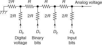
Fig. 10.12 Binary Ladder Network Containing R-2R Resistors
10.9 BINARY WEIGHTED RESISTOR TYPE DIGITAL TO Analog CONVERTER
A binary weighted resistor DAC network consists of the following components:
- One op amp
- Binary weighted resistor network consisting of several resistors starting from R, 2R, 4R, 8R, …, 2NR depending upon the number of data bits (N) used in the DAC
- Voltage inputs to the DAC network
- Reference voltage VR
- Final analog output voltage Vout corresponding to the digital input
For ON switch, current I = ![]() , and for OFF switch, current I = 0 (zero).
, and for OFF switch, current I = 0 (zero).
From the schematic diagram shown in Fig. 10.13, IF = I1 + I2 + I3 + I4+ …, where ![]() and so on.
and so on.

Fig. 10.13 Binary Weighted Digital to Analog Converter Circuit Using Operational Amplifier
Voltage across RF is the output voltage Vout, where
Vout = − IF × RF = [I1 + I2 + I3 + I4 + ….] × RF
The output voltage can also be expressed in terms of weightage for the positions of 1 and 0 bits of binary word as follows:
Output voltage Vout = − (2(N − 1) × V(1) + 2(N − 2) × V(2) + 2(N − 3) × V(3) + 2(N −4) × V(4))
For the considered 4-bit word, this expression becomes as follows (N = 4):
Vout = − (2(4 −1) × V(1) + 2(4 −2) V(2) + 2(4 −3) × V(3) + 2 (4 −4) × V(4))
Therefore,
Vout = − (2(3) × V(1) + 2(2) × V(2) + 2(1) × V(3) + 2(0) × V(4))
Vout = − (8 × V(1) + 4 × V(2) + 2 × V(3) + 1 × V(4))
Substituting the expressions for currents in terms of input data binary voltages,
Output voltage Vout = − (8 × V(1) + 4 × V(2) + 2 × V(3) + 1 × V(4))
Example 10.11
Calculate the magnitude of analog output voltage for the weighted resistor DAC circuit shown in Fig. 10.13 for binary data word of 1010 applied at its input. Assume logical 1 = 1 volt and logical 0 = 0 V for the DAC.
Solution: Vout = − (8V(1) + 4V(2) + 2V(3) + V(4))
Data: Binary data word is 1010. It represents the following voltages:
V(1) = 1 V, V(2) = 0 V, V(3) = 1 V, and V(4) = 0 V
Output voltage Vout = − (8 + 0 + 2 + 0) = 10 V
10.10 R-2R LADDER WITH OPERATIONAL AMPLIFIER TYPE DIGITAL TO Analog CONVERTER
Conversion of digital voltage to analog voltage can be done in different methods, of which one is by using a ladder network of resistors. Summing amplifier using op amp and ladder network consisting of R-2R elements convert a binary digital signal into an analog signal. DAC circuit looks similar to a ladder containing R-2R circuit elements. Hence, the circuit is known as an R-2R ladder type DAC.
Principle of Operation
This DAC works on the following principle of operation:
- Digital input voltages are of two levels: logical 1 and logical 0. When the FET switch closes on logical 1, it has a voltage of 2−5 V. When the switch operates on logical 0, the voltage level is 0 volts. It uses switching (Boolean) algebra, introduced by Shannon.
- Voltages of magnitude Vref or 0 V work as data input signals. They are represented as D0, D1, D2, D3 (four input voltages) and so on up to Dn to the R-2R ladder network connected to the summing amplifier shown in Fig. 10.14.

Fig. 10.14 Digital to Analog Converter Using Summing Amplifier
- Four input voltages are considered as four data inputs to the DAC circuit. The circuit in Fig. 10.14 is for four digital data input bits, but it can be extended to any number of bits up to Dn.
- FET device switches are used for switching the voltages between logic 1 and logic 0 levels in the network. (FET devices are used for matching very high input impedance between the stages and lower values of leakage currents.) If any one of the digital input Vin = 1, the voltage Vref is connected to the input end of the appropriate resistor. The reference voltage Vref could be VDD (drain supply voltage) for FET devices or VCC (collector supply voltage) for BJT devices.
- The output voltage of the op amp is the output of the DAC circuit.
Output voltage
 volts (DC voltage)
Example 10.12
For the given input voltages of D0 = Vin(0) = 0, D1 = Vin(1) = 1, D2 = Vin(2) = 0 and D3 = Vin(3) = 1, Vref = 8 V, calculate the DC output voltage.
Solution:
DC output voltage  = 5 V
= 5 V
Advantages
- There are only two types of resistors: R and 2R.
- The ratio of the resistors is more important than their actual values.
- Using only two types of resistors in the circuit works well for realization in IC form.
- There is better accuracy.
Disadvantages
- Currents through the resistors change with changes in binary voltages applied to them.
- Currents through the resistors develop heat in them due to power dissipation. This disadvantage is minimized by changing the orientation of the R-2R ladder structure as in an inverted R-2R ladder DAC.
10.11 INVERTED R-2R LADDER DIGITAL TO Analog CONVERTER
The following observations could be made by comparing Fig. 10.14 showing an R-2R ladder network and Fig. 10.15 showing an inverted R-2R ladder network:

Fig. 10.15 Digital to Analog Converter Using Inverter R-2R Ladder and Summing Amplifier
- The binary bit positions of the digital inputs are interchanged.
- Each of the binary inputs Vin(0), Vin(1), Vin(2), and Vin(3) is connected through the resistors to one end of the corresponding switches. The other end of these switches is connected to the negative input terminal of the op amp when the binary bit is in one (1) state.
- The negative input terminal of the op amp is also at virtual ground (GND in the Figure) for practical purposes.
- The other end of the resistors is connected to the ground terminal when the binary bit is in zero (0) state.
- The switching nodes in the two positions are at ground potentials. Hence, the parasitic capacitances associated with switching are minimized, and consequently, this DAC works faster than the other types of DACs.
The four input voltages can be considered as follows:
Vin(0) = D1
Vin(1) = D2
Vin(2) = D3
Vin(3) = D4
Then, the output voltage ![]()
Example 10.13
Calculate the magnitude of the analog output voltage for the inverted R-2R ladder network DAC circuit shown in Fig. 10.15 for binary data word of 1010 applied at its input. Assume that logical 1 = 1 V and logical 0 = 0 V for the DAC. The reference voltage Vref = 16 V.
Solution: ![]()
Data: D1 = 1 V, D2 = 0 V, D3 = 1 V, and D4 = 0 V
Substituting the data in the equation: ![]() = 5 V
= 5 V
10.12 DIGITAL TO Analog CONVERTER WITH MEMORY
The schematic diagram of a DAC with memory is shown in Fig. 10.16.

Fig. 10.16 Digital to Analog Converter Circuit with Memory
Digital data input samples (binary data) are connected to a memory unit such as D flip-flop registers. The outputs of the registers are connected to the ladder network and the op amp in the DAC. The flip-flops hold the input digital data as per the design for a specified time. The digital input signals move to the DAC after some (designed) delay in the memory registers. Then, the DAC converts the digital sample voltages to analog signal output. Finite time delay occurs for the analog output signal to respond to the digital signals at selected time instants.
Whenever a DAC circuit is needed to give outputs at desired time instances for the digital input samples, a memory circuit is incorporated before the DAC.
Application: A DAC circuit is used to convert the digital signal output from the computers into analog signals for use by X-Y plotters and recorder instruments.
10.13 IC 1408/1508 DIGITAL TO Analog CONVERTER
Motorola IC 1408/1508 DAC is an 8-bit DAC. It is available in dual inline package. It offers highly stable performance at low cost and with advanced circuit design.
The following are the main components of an IC 1408 DAC:
- Reference voltage source at pin 15 to supply the total reference current
- R-2R ladder network to split the reference current into binary components corresponding to the binary data inputs D0 to D3
- High-speed switches (8) corresponding to each binary input for digital to analog conversion
- Current-to-voltage converting op amp to convert analog output current to output voltage
Figure 10.17 provides the pin diagram details of a DAC 1408 IC. The following can be observed from the Figure:

Fig. 10.17 Pin Diagram Details for DAC 1408 IC
- Input binary sequence is given to pins 5−12.
- The LSB is connected to pin 12.
- The MSB is connected to pin 5.
- The supply voltage is between pins 2 (GND) and 13 (+V CC of 5 volts).
- The output of the DAC is the current output from pin 4. Using a current-to-voltage converter op amp, output current is converted to output voltage (Vout) representing the magnitude of the analog voltage to digital input to the IC.
Applications
- Sample and hold circuits
- Digital voltmeters and digital panel meters
- Speech signal processing
- Servo motor applications
- Digital filters
10.14 SPECIFICATIONS FOR INTEGRATED CIRCUITS USED IN DIGITAL TO Analog CONVERTERS AND Analog TO DIGITAL CONVERTERS
For better ESDM processes, the inner circuit details of the different types of ADC ICs and DAC ICs are to be understood clearly. Before the selection of an IC, its specifications are more useful for the system design.
- Temperature range and electrical and mechanical specifications for the following types of applications:
- Commercial
- Industrial
- Military
- Type of IC package and number of pins:
- Dual inline package
- Metal casing
- Plastic
- Architecture of the internal circuit:
- Dual slope integrator type ADC
- R-2R ladder type network
- Parallel (flash)
- Interface type at the output port of the IC:
- Serial port interface
- Parallel port interface
- Input terminal types:
- Single-ended pair of input terminals
- Differential input terminals
- Multiple inputs
- Sampling rates of input signals—555 KHz (typical value)
- Operating voltages and currents:
- Operating voltages: 3 V or 5 V
- Operating current: 1.25 mA (typical value)
- Supply voltage variations
- Power dissipation
- Temperature variations, as they affect converter performance features
- Interfacing capability with other devices
- Resolution
- Conversion time, which is the total time taken for the analog to digital signal conversion and propagation delays in the total circuit of the ADC
- Linearity
- Number of binary digital display for the ADC—4-bit display (typical value)
- Zero offset
- Accuracy, which is the difference between the expected output and the actual output (e.g., in DAC, accuracy will be defined in terms of the difference between the estimated analog output voltage and the measured output voltage)
- Quantization error, which is associated only with ADC circuits
- Settling time in high-speed data converters, which is the time taken for the output voltage to settle down at the final response within a specified error band for step voltage input and is caused by propagation delay
- Stability
POINTS TO REMEMBER
- A transducer or sensor converts a signal from one form of energy into another form. One familiar example is the microphone, which converts acoustic or speech energy into electrical energy as an electrical signal. A similar transducer is the loud speaker, which converts the electrical signal into speech or acoustic energy. Signal conditioning is done for measurement and control operations.
- Analog signal is converted into digital signal in the form of binary words, using the processes of sampling quantization. Binary words are applied to a binary counter and a seven-segment display. The strength of the analog signal is shown as the digital display.
- Analog to digital signal conversion using flash type ADCs is very fast. Therefore, they are more popular in high-speed electronic circuits. Flash type ADCs are also called parallel or simultaneous comparator ADCs.
- Resolution is the number of analog output values that can be produced by an n-bit DAC.
- Resolution R = 2n
- For a 1-bit DAC, resolution R = 21 = 2 levels
- For an 8-bit DAC, resolution R = 28 = 256 levels
- Actual resolution is related to the effective number of bits.
- There are two types of ADCs:
- Direct type ADCs: Examples are counter type (tracking type) ADC, flash type ADC, and SA type ADC.
- Indirect type ADCs: Examples are single slope integrating type ADC and dual slope integrating type ADC. The analog input signal is converted to a signal that is a linear function of time. Then, it is converted to digital data.
- A DAC converts n-bit binary words into proportional analog signal (voltage).
- Basic circuits used for converting digital signals into analog signal output are as follows:
- Operational amplifier with R-2R ladder network and electronic switches
- Binary weighted resistors, switches, and op amps
- Telephone calls in simplex and duplex systems use both ADCs and DACs with relevant transducers in total channels.
- Voltage resolution of an ADC =
 , where n is the number of bits converted by the ADC and VFS is the full-scale voltage.
 - Percentage resolution of an ADC =

- Maximum frequency fmax of a sine wave that can be digitized is expressed by the following equation:
 Hz
Hz where
n = number of bits used for conversion
TC = conversion time to undergo analog to digital conversion process
- Salient features of ADC and DAC circuits are as follows:
- Temperature range and electrical and mechanical specifications for commercial, industrial, and military applications
- Type of IC package and number of pins, such as dual inline package, metal casing, and plastic packaging
- Architecture of internal circuit, such as dual slope integrator type ADC, R-2R ladder type network, and parallel (flash)
- Interface type at output port of IC, such as serial port interface and parallel port interface
- Power dissipation
- Interfacing capability with other devices
- Resolution
- Conversion time
- Linearity
- Settling time in high-speed data converters
- Stability
SUMMARY
- Basic principles of operation of analog to digital signal conversion are explained. An analog signal is converted to a digital signal in the form of binary words. The binary data can be displayed and made available for further use.
- Analog to digital converter circuits are of two categories:
- Direct type ADCs such as parallel comparator (Flash) ADC, counter type ADC, and SA type ADC
- Integrating type ADCs such as single slope type ADC and dual slope type ADC
- Circuit working of various types of DAC circuits are explained with necessary diagrams.
- A DAC circuit is used to convert digital data representing binary bits into analog data.
- Operational amplifiers and resistor networks are used to convert binary (digital) signals into analog signals in (a) binary weighted DACs, (b) R-2R ladder network DACs, and (c) inverted R-2R ladder type DACs. Such circuits are explained with neat circuit diagrams.
QUESTIONS FOR PRACTICE
- Write short notes on (a) ADC and (b) DAC circuits and mention a few applications for each.
- Draw the circuit of a parallel comparator (flash) type ADC and explain its operation. Mention the main advantage of the flash type ADC.
- Draw the circuit of a counter type ADC and explain its operation.
- Draw the circuit of an SA type ADC and explain its operation.
- (a) Describe the various blocks in a single slope type ADC. (b) Explain the method of conversion of analog to digital signals and the process of measurement of the analog signal using this type of ADC.
- (a) Describe the various blocks in a dual slope type ADC. (b) Explain the method of conversion of analog to digital signals and the process of measurement of the analog signal using this type of ADC.
- Explain the method of obtaining an analog voltage proportional to the digital signal applied (binary input) to a binary weighted resistor DAC. Describe the relevant circuit to achieve digital to analog signal conversion using an op amp.
- Explain the role and operation of an op amp in the conversion of digital input to analog output using an R-2R ladder DAC circuit.
- Draw the circuit of an inverting R-2R ladder type DAC and explain the method of conversion of digital to analog signals.
- Calculate the magnitude of the analog output voltage for the weighted resistor DAC circuit shown in the Fig. 10.13 for binary data word of 1111 applied at its input. Assume logical 1 = 1volt and logical 0 = 0 V for the DAC.
- Explain the working of a DAC using a memory unit.
- A counter type ADC uses a 4-bit counter and clock signal frequency of 1 MHz. Calculate the (a) resolution and (b) conversion time.
- (a) Find the resolution of a 12-bit DAC. (b) List the drawbacks of a binary weighted resistor technique of digital to analog conversion. (c) Explain the working of an R-2R ladder DAC.
- Explain the operation of an 8-bit tracking type ADC.
- Compare the conversion times and efficiencies of an 8-bit tracking type ADC and a SA type ADC.
- Compare the conversion times and hardware complexities of various ADC circuits.
- Compare an R-2R ladder type DAC and a weighted resistor type DAC.
- Write short notes on ADCs.
MULTIPLE-CHOICE QUESTIONS
- Maximum conversion time for analog to digital signal conversion in SA type ADC
Ans. (a)]
- Maximum conversion time for analog to digital signal conversion in staircase ADC
Ans. (b)]
- Voltage resolution of an ADC with number of bits n = 12 and full-scale deflection voltage VFS = 20 V
- 4.884 mv
- 2.442 mv
- 3.662 mv
- 6.1 mv
Ans. (a)]
- Voltage resolution of an ADC with number of bits n = 12 and full-scale deflection voltage VFS = 10 V
- 4.884 mv
- 2.442 mv
- 3.662 mv
- 6.1 mv
Ans. (b)]
- Voltage resolution of an ADC with number of bits n = 12 and full-scale deflection voltage VFS = 15 V
- 4.884 mv
- 2.442 mv
- 3.662 mv
- 6.1 mv
Ans. (c)]
- Percentage resolution of an ADC with binary digits of n = 8
- 0.391
- 6.25
- 0.0244
- 2328 × 10−9
Ans. (a)]
- Percentage resolution of an ADC with binary digits of n = 12
- 0.391
- 6.25
- 0.0244
- 2328 × 10−9
Ans. (c)]
- Percentage resolution of an ADC with binary digits of n = 4
- 0.391
- 6.25
- 0.0244
- 2328 × 10−9
Ans. (b)]
- Voltage resolution of an ADC with output voltage range of 20 volts and binary digits n = 12
- 99.99 mv
- 33.33 mv
- 6.66 mv
- 4.88 mv
Ans. (d)]
- Analog to digital signal conversion time TSA ADC for a 12-bit SA type ADC with clock frequency of 3 MHz
- 4 μ s
- 2 μ s
- 3 μ s
- 5 μ s
Ans. (a)]
- Analog to digital signal conversion time TSA ADC for a-10 bit SA type ADC with clock frequency of 5 MHz
- 4 μ s
- 2 μ s
- 3 μ s
- 5 μ s
Ans. (b)]
- Analog to digital signal conversion time TSA ADC for a 16-bit SA type ADC with clock frequency of 4 MHz
- 4 μ s
- 2 μ s
- 3 μ s
- 5 μ s
Ans. (a)]
- Disadvantage of a parallel comparator type ADC
- Number of bits increases as complexity of signal increases
- Divider network needs a large resistive network
- Requirement of comparators doubles with increase of every bit
- All of these
Ans. (c)]
- Fastest ADC
- Dual slope ADC
- Flash type ADC
- Counter type ADC
- Single slope type ADC
Ans. (b)]
- Low-speed ADC
- Dual slope ADC
- Flash type ADC
- Counter type ADC
- SA type ADC
Ans. (d)]
- Drawback of a dual slope ADC
- High cost
- Complex circuit
- Long conversion time
- All of these
Ans. (d)]
- Advantage of a dual slope type ADC
- Accurate measurement of slowly varying signals
- Fast conversion process
- Long conversion time
- Excellent noise rejection
Ans. (a)]
- Resolution of an 8-bit DAC
- 8
- 16
- 64
- 256
Ans. (d)]
- Resolution of a 4-bit DAC
- 4
- 8
- 16
- 32
Ans. (c)]
- Resolution of a 1-bit DAC
- 4
- 8
- 16
- 2
Ans. (d)]