
Carbon-Nanotube Solutions for the Post-CMOS-Scaling World
IBM Research, SRDC, T. J. Watson Research Center Yorktown Heights, NY 10598, U.S.A.
1. Introduction
The CMOS research world has been up-ended in the past few years with the realization that the end of scaling is indeed approaching fast1 and that other, more radical solutions need to be found. Much work has been focused on investigating a radical (for CMOS) set of new materials, strain engineering, and new geometries such as two-dimensional (2D) electrostatically confined structures and 3D heterogeneous integration. These approaches extend the technology and provide a more powerful end-point, but do not drastically alter the scaling scenarios. The capabilities projected for future CMOS are enormously larger than even today’s gigascale integrated circuit (IC) chips, so the question arises as to the need for any CMOS follow-on at all. An interesting feature, pertaining especially to the silicon-on-insulator (SOI) approaches, is that the “silicon” technology is becoming divorced from the bulk silicon material. Indeed, for these technologies any convenient material could, in principle, be used for the substrate.
Of the various alternative “nano-offerings” investigated in the past few years,2,3 none can be seen as a serious competitor to ultimate CMOS. Device characteristics are poor, unreliable and noisy, and manufacturing methodologies are uncertain at best. A possible exception, at least in terms of the intrinsic device, is the carbon nanotube. Carbon nanotubes (CNTs) can be thought of as the perfect electron waveguides, where electrons can be transported through unimaginably small channels without scattering off the boundaries. In addition, phonon interactions are weak. This results in transport properties far superior to silicon per unit channel area, with the additional advantage that these properties are symmetric for both p and n channel transport. However, challenges to implementing this technology and realizing these intrinsic advantages in terms of system performance are formidable. Firstly, how do we place, or grow, CNTs of desired properties on the circuit substrate. Then, given such placement, how do we fabricate FETs with specific and tightly controlled characteristics, and with low parasitic capacitances and resistances? Last, but not least, how do we best use CNTs in circuits and systems, and what performance advantages are expected.
2. Intrinsic properties
It is for their intrinsic properties as an FET that CNTs arouse the most excitement in those looking for future CMOS solutions. Scaling limitations of MOSFETs due to boundary scattering of electrons from imperfect interfacesds4,5 are solved naturally in CNTs, as they have a smooth, well-coordinated graphene structure6 with no bonds to the outside. This enables CNTs to retain excellent transport properties down to much smaller lateral dimensions than silicon. Their small radius and the possibility of completely surrounding the CNT by a gate can provide excellent electrostatic confinement of the channel electrons, enabling the channel length to be scaled down to very small dimensions. Their small size would enable high packing densities. Bandstructure calculation6,7 of CNTs show that conduction and valence bands are mirror images of each other, i.e. both electrons and holes should share equally good transport properties. This indicates the suitability of CNTs for a general-purpose high-performance complementary circuit technology.
As is now well known, CNTs can be either metallic or semiconducting, depending on their chirality,6,7 and the semiconducting tubes have a bandgap EG that is inversely proportional to their diameter dCNT. Specifically, tight binding calculations lead to the following useful relation between dCNT and bandgap EG:
where γ is the hopping matrix element and dCC is the carbon-carbon bond distance. Inclusion of electron-electron interactions increases EG significantly,6 and for a 1 nm nanotube the bandgap is roughly 1 eV. From an FET scaling perspective, a large bandgap is desirable to minimize band-to-band tunneling, as well as the tunneling breakdown of the drain contact that can result in undesirable ambipolar8 characteristics. In practice, however, the best transport measurements and device characteristics have been obtained on rather larger diameter nanotubes, in the dCNT = 1.7–3 nm range. The idealized electron/hole dispersion relation is hyperbolic in shape, with a quasi-parabolic “effective mass” regime at lower energies and a linear “constant velocity” regime at higher energies, where the limiting velocity vlim reaches ~5–10×107 cm/s.9
Transport properties are further enhanced by the weak coupling of the charge carriers to acoustic phonons and the fact that the optical phonons have large energies of ~0.15eV.10 All of these factors lead to extraordinarily large mobilities, reported at ~105 cm2/V·s at room temperature!11 Granted, as we have learned over the years from development of circuit technologies using III-V materials, high mobilities do not lead to proportionate increases in device and circuit performance. Nevertheless, the high mobility of CNTs is an important factor in estimating their overall performance.
Unlike in silicon, reliable doped contacts for CNTs are not available, and contacts are typically made using Schottky-barrier metals. For instance Pd will make p-type and Al n-type contacts12 to CNTs. To date, good contacts have only been made to CNTs of diameter ~1.7 nm and larger, which have bandgaps less than ~0.7 eV. These smaller band gaps pose a problem for FETs. Since they lower the Schottky barrier height for both electrons and holes, while they permit good contacts for the one carrier type at the source, they also permit tunneling of the opposite type of carriers at the drain. This is the “ambipolar” effect8 and is deleterious because it opens a path for flow of the opposite carrier type under conditions where the FET should be switched off.
The CNT band-structure, while facilitating electron and hole transport, also facilitates band-to-band tunneling.13 Band-to-band tunneling in FETs is only operative when conduction and valence bands are brought into alignment, i.e. when the bandgap is comparable to or less than the supply voltage (~1 V). This places a technological premium on being able to successfully contact small diameter CNTs.
3. Device and circuit benchmarks
The CNT technology is still at a very primitive state where, for the most part, placement, CNT type (metallic or semiconductor), and diameter and length of the nanotubes cannot be controlled.6 Devices and circuits are made, for the most part, by building devices around existing tubes, or blindly fabricating large arrays of structures and picking the statistically good ones.
Typically, e-beam lithography is used in the former approach because of its flexibility in shaping patterns around existing tubes. Important benchmarks have been established. The first CNT FETs14 were p-FETs using a silicon wafer as a back-gate. Complementary circuits have been made with selective doping.15 In another approach, both p and n-type FETs16 have been demonstrated with tens of microamps of current per tube, using Pd contacts for the p-type and Al contacts for the n-type FETs. A transconductance gm of 26μS has been achieved, which is to be compared with the maximum possible theoretical transconductance of 167μS,17 for the ground-state subband of a single tube. Once the gate and drain voltages go above ~0.5 V, optical phonon emission can limit device current.20 Self-aligned Pd source/drain contacts were demonstrated19 as a means of minimizing parasitic capacitance. An integrated ring-oscillator has been made,21 with all of the circuits laid out along a single CNT. The ring oscillator achieved an average delay of down to 2 ns per stage, but this delay reflected mainly the parasitic overlap and wiring capacitance contributions rather than the intrinsic speed of the CNT itself. High frequency measurements have also been made on C NTs,22 but care should be taken in interpreting these results, because of parasitics and contact effects.
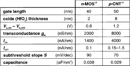
Table 1. Best of breed, n-MOS vs. p-CNT. The IOFF in p-CNT is limited by ambipolar conduction at VD = 0.3 V.
4. Manufacturing paradigm: Top down or bottom up?
For the CNT to succeed as a technology it has to overcome the placement, diameter and type selection problems. While work is proceeding in growing nanotubes in-situ, from placed catalysts,6 it seems that there might be a more elegant way to solve this problem, leading to a very different paradigm for integrated circuit manufacture. Today’s paradigm would prepare locations on a semiconductor chip, grow nanotubes in these locations, coat them with dielectrics, gate metals etc. and then lithographically define the nanotube FETs. The new approach would be to disperse the nanotubes in solution (liquid or gas), filter them according to type, diameter and length, coat them with dielectric and perhaps metal layers, and then deposit them in prepared locations on the IC chip. Subsequently the rest of the FET, including source and drain contacts, are made using conventional IC fabrication techniques. The advantages are not only that of a mass fabrication and selection process, but also that dielectric and metal layers are easier to coat conformally on a CNT while it is in solution, than when it is already lying on a substrate. Furthermore, the coating process provides a natural way of separating the nanotubes, so they might be stacked next to each other on the substrate. While this scheme in all its details has not been articulated previously, to my knowledge; parts of it are subjects of active research, such as filtration techniques for nanotubes in solution,23 methods of conformal coating of CNTs in solution,24 and methods of placing CNTs in pre-determined locations.6 These might well lead to an exciting revolution in future IC technology.
5. Ballistic transport
In this section we examine fact and fiction, opportunities and pitfalls, concerning ballistic transport. The intrinsic properties of CNTs make them good candidates for ballistic transport, and several signatures for ballistic transport have been reported.20,25,26 Ballistic transport is uncritically thought to lead to large improvements in device performance, but in reality it matters little, in terms of device current, whether carriers have or have not scattered a few times in transiting the channel. Figure 1 illustrates a situation where carriers are either partially or fully ballistic – Fig. 1(a) and (b), respectively. One sees that the current injected into the channel is about the same, while the charge in the ballistic channel has been reduced because of the absence of back-scattering and scattering to lower energies. Thus the performance is improved. This advantage is lost, however, in switching from the “on” state27 to the “off” state, because when the transistor is on and VD = 0, both directions are fully occupied – see Fig. 1(c).

Figure 1. Ballistic transport: schematic band diagram showing half-degenerate state occupancy for large drain bias with partially (a) or fully (b) ballistic transport in the channel; (c) shows full occupancy at zero drain bias.
Ballistic transport is seen as a panacea to avoid energy loss. In a transistor, even with a ballistic channel, dissipation in the drain contact provides a dissipation mechanism. However, it is instructive to consider a case where this mechanism is absent. If there were no contact with the thermal bath, could not computation be dissipationless? We will not debate the broader issue28 here, but concentrate on a simple logic transition involving the discharge of a capacitor through a transistor, illustrated in Fig. 2. The whole system could, in principle, be ballistic since both capacitor and transistor could be part of the same CNT, eliminating the drain contact. The charged capacitor is represented by an empty potential well. Were the system lossy, the capacitor would discharge as the potential well filled up. For a purely ballistic system, however, the electrons from the source cannot thermalize into the well and are reflected back. The above example is a cautionary lesson that, contrary to expectations, ballistic transport might well slow down logic transitions.

Figure 2. Discharge of a ballistic capacitor through a ballistic FET: transistor is off in (a) and on in (b) and (c); (b) is non-ballistic while (c) is ballistic.

Table 2. Analogy between a ballistic conductor and a transmission line.
Table 2 illustrates an interesting analogy between a ballistic system described by a limiting velocity vlim and an electromagnetic transmission line, for the case where the capacitance is dominated by the intrinsic quantum capacitance29 of the CNT wire, rather than the gate capacitance.30 In Table 2, r0 = h/4e2.17 Both the quantum capacitance and kinetic inductance31 are accounted for in this analogy. The resistance r0 is usually described as a contact resistance, but a more correct description is wave impedance, since it is a non-local property of the traveling electron wave rather than a local property of the contact. Like its electromagnetic counterpart, the wave impedance characterizes the impedance under pulsed conditions and the dc input resistance will be influenced by reflections from the far contact. Although instructive, this analogy is not perfect. While electrons may be reflected from a barrier at the far end, this does not cause voltage doubling, as in an electromagnetic transmission line, but rather charge doubling, because now states below the Fermi level are filled by electrons traveling in both directions. Further, there is no easy equivalent to a shorted transmission line, where reflections are negative.
The kinetic inductance plays a major role if one tries to use nanotubes as interconnects.32 It is larger than the electromagnetic transmission line inductance by the ratio of Z0vlim/r0c. This is a very large ratio since r0 >> Z0 (by a factor of ~120) and c >> vlim (by a factor of ~300). Whether the line acts as a resistor or as an inductor depends on the time scale, set by L/R. For a ballistic line, this time scale is l/vlim, where l is the line length, otherwise it is set by the momentum relaxation time τp. Since most switching times are expected to be longer than τp (~6 ps for a mobility of 105 cm2/V·s) the inductance, though large, would be unimportant compared to the wire’s resistance. For long wires, many nanotubes would have to be bundled together (or thicker, multiwalled nanotubes6,31 should be used), which would reduce both the resistance and the inductance.
The same arguments apply to the use of kinetic inductors as part of resonant systems, for instance in energy recovery circuits. For most applications where the operating frequency f << 1/τp, the Q of the inductor will be low and not much will be gained.
The ballistic nature of transport in nanotubes does introduce the possibility of new types of solid-state devices. For example, the correlated nature of ballistic transport can be used to achieve amplification at frequencies well beyond transit-time limitations. These are the direct descendents of vacuum tubes, where ballistic transport is the norm, but on a vastly smaller scale. A schematic of such a device, along with a crude ballistic simulation, is shown in Fig. 3. The simulation shows that the kinetic energy in the channel may be increased beyond the applied gate voltages by suitably timing the gate signals with respect to the ballistic transit time between gates. When distances between gates are less than 1 μm, terahertz amplification might be possible.
6. Logic applications
Looking toward the future, both CMOS and CNT transistors will be scaled toward their limits,1 although, for practical reasons, they will stop well short of their ultimate limits. A schematic drawing of the active areas of these hypothetical devices is shown in Fig. 4, with the corresponding electrical parameters given in Table 3. End capacitances have been estimated by assuming 5 nm silicon dioxide end-spacers for the CNTs. These parameters are realistic for CMOS but are “best case” for CNTs. since at present such high currents cannot be extracted from 1 nm sized CNTs.
We see that the current drive of ultimate CMOS and CNTs is comparable, but the CNT has a much lower capacitance and a somewhat lower operating voltage. The CNTs may be organized into logic arrays33 stacked side by side to make use of their higher intrinsic packing density. Even a short length of wire will overwhelm the ~10aF gate (including ends) capacitance of the CNT. Typical wire capacitance is ~0.2aF/nm so that a wire length of greater than ~50 nm will already dominate the capacitance. So where is the advantage of CNTs over CMOS?
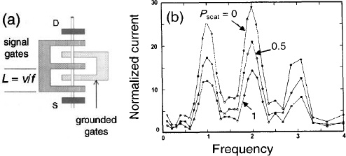
Figure 3. Traveling-wave type ballistic device: (a) schematic layout and (b) simulation showing the normalized output current vs. frequency in units of inverse transit time between the gates, parametrized by the scattering probability Pscat per transit between two signal gates.

Figure 4. Active areas of CMOS and CNT transistors extrapolated to the future.
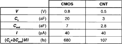
Table 3. Intrinsic parameters of scaled FETs.
In today’s power constrained environment, achieving competitively high performance at a low switching energy per logic transition is more important than achieving the highest switching frequency. In general the dynamic switching energy U is given by
where Cdev and Cwire are the device and wiring capacitance contributions, respectively. To minimize U, minimum-sized devices and corresponding interconnect lengths should be used, as well as the minimum supply voltages consistent with ensuring an acceptable on/off current ratio. Here the CNT has a considerable advantage, of up to a factor of ~6, because of its smaller intrinsic capacitance and size. The trade-off between switching energy and performance can be examined in more detail by considering the CMOS switching energy vs. transition rate plot as modeled by Frank and co-workers,34 where we have superimposed some hypothetical CNT curves – see Fig. 5. In CMOS, the switching energy increases with switching rate for two main reasons. Firstly, to drive the wires at higher speeds, wider FETs with larger capacitance have to be used. This not only increases Cdev, but also Cwire, because of lower device density. Secondly, because of the low CMOS mobility, voltages have to be increased to get the speed. For CNTs, the device size is small, so that wire lengths will be shorter; the intrinsic capacitance is so small that devices may be added in parallel to get more current without impacting the overall capacitance much; and because of the high CNT mobility, voltages do not have to be increased get higher speeds. These properties are illustrated by means of the superimposed curves in Fig. 5. The curve marked A assumes the same wire length and voltage (at low performance) as CMOS, but the smaller intrinsic capacitance of the CNT and constant supply voltage enables one to stay at the “low performance” switching energy up to much higher switching rates than CMOS. Furthermore, as shown by curve B, when these constraints are relaxed, the CNT benefits further, i.e. the starting switching energy is lower because of the shorter wire length and lower voltage. Thus, the most competitive arena for CNT logic is at roughly the same performance as high performance CMOS, but with much lower switching energies.

Figure 5. Loaded switching energy vs. logic transition rate for a CMOS processor core (adapted from Ref. 34).
7. Conclusions
The CNT is a revolutionary device because, for the first time, the dimensions of the conducting channel are controlled by chemical bond lengths and not by some arbitrary manufacturing process. Electron transport down a nanotube is extraordinary. To make the CNT a contender in the post-CMOS arena, difficult challenges have to be overcome and hard questions need to be answered concerning the integration CNTs onto an IC chip, the contacting of small diameter CNTs, and the elimination of ambipolar conduction. The small size and low capacitance of CNTs lend them to the critical area of logic applications at low switching energy. The expected ballistic nature of transport at sub-micrometer dimensions opens up opportunities for unique high frequency applications in the THz regime.
Acknowledgments
I wish to acknowledge the help of the following in the form of discussions and material supplied: Tom Theis, Phaedon Avouris, Joerg Appenzeller, Zhihong Chen, Yu-Ming Lin and David Frank.
References
- W. Haensch, E. J. Nowak, R. H. Dennard, et al., “Silicon CMOS devices beyond scaling,” IBM J. Res. Dev. 50, 339 (2006).
- S. Luryi, J. M. Xu, and A. Zaslavsky, eds., Future Trends in Microelectronics: The Nano, the Giga, and the Ultra, New York: Wiley, 2004.
- ITRS “Emerging Research Devices” (2005), www.itrs.net/Links/2005ITRS
- T. Ando, A.B. Fowler and F. Stern, “Electronic properties of two-dimensional systems,” Rev. Mod. Phys. 54, 437 (1982).
- K. Uchida, H. Watanabe, A. Kinoshita, J. Koga, T. Numata, and S. Takagi, “Experimental study on carrier transport mechanism in ultrathin-body SOI n-and p-MOSFETs with SOI thickness less than 5 nm,” Tech. Digest IEDM (2002), pp. 47–50.
- An excellent review carbon nanotube theory, devices and technology can be found in: P. Avouris and J. Chen, “Nanotube electronics and optoelectronics,” Mater. Today 9, 46 (2006).
- J. W. Mintmire, D. H. Robertson, and C. T. White, “Properties of fullerene nanotubules,” J. Phys. Chem. Solids 54, 1835 (1993).
- V. Derycke, R. Martel, J. Appenzeller, and P. Avouris, “Controlling doping and carrier injection in carbon nanotube transistors,” Appl. Phys. Lett. 80, 2773 (2002).
- G. Pennington and N. Goldsman, “Semiclassical transport and phonon scattering of electrons in semiconducting carbon nanotubes,” Phys. Rev. B 68, 045426 (2003); Yung-Fu Chen and M. S. Fuhrer, “Electric-field-dependent charge-carrier velocity in semiconducting carbon nanotubes,” Phys. Rev. Lett. 95, 236803 (2005).
- V. Perebeinos, J. Tersoff, and P. Avouris, “Electron-phonon interaction and transport in semiconducting carbon nanotubes,” Phys. Rev. Lett. 94, 086802 (2005).
- T. Dürkop, S. A. Getty, Enrique Cobas, and M. S. Fuhrer, “Extraordinary mobility in semiconducting carbon nanotubes,” Nano Lett. 4, 35 (2004).
- Z. Chen, J. Appenzeller, J. Knoch, Y. Lin, and P. Avouris, “The role of metal-nanotube contact in the performance of carbon nanotube field-effect transistors,” Nano Lett. 5, 1497 (2005).
- J. Appenzeller, Y.-M. Lin, J. Knoch, and P. Avouris, “Band-to-band tunneling in carbon nanotube field-effect transistors,” Phys. Rev. Lett. 93, 196805 (2004).
- R. Martel, T. Schmidt, H. R. Shea, T. Hertel, and P. Avouris, “Single- and multi-wall carbon nanotube field-effect transistors,” Appl. Phys. Lett. 73, 2448 (1998).
- V. Derycke, R. Martel, J. Appenzeller. and P. Avouris, “Carbon nanotube inter- and intramolecular logic gates,” Nano Lett. 1, 453 (2001).
- A. Javey, Q. Wang, W. Kim, and H. Dai, “Advancements in complementary carbon nanotube field-effect transistors,” Tech. Digest IEDM (2003). pp. 31.2.1–4.
- This value comes from 4e2/h, with a factor of 2 arising from the two-fold degeneracy of the lowest bands and the other factor of 2 from the spin degeneracy.
- J. Kavalieros, B. Doyle, S. Datta, et al., “Tri-gate transistor architecture with high-κ gate dielectrics, metal gates and strain engineering,” Tech. Digest VLSI Symp. (2006), pp. 50–51.
- A. Javey, D. Farmer, R. Gordon and H. Dai, “Self-aligned 40 nm channel carbon nanotube field-effect transistors with subthreshold swings down to 70 mV/decade,” Proc. SPIE 5732, 14 (2006).
- A. Javey, J. Guo, M. Paulsson, Q. Wang, D. Mann, M. Lundstrom, and H. Dai, “High-field quasiballistic transport in short carbon nanotubes.” Phys. Rev. Lett. 92, 106804 (2004).
- Z. Chen, J. Appenzeller, Y-M. Lin, et al., “An integrated logic circuit assembled on a single carbon nanotube,” Science 311, 1735 (2006).
- D. V. Singh, K. A. Jenkins, J. Appenzeller, D. Neumayer, A. Grill, and H. S. P. Wong, “Frequency response of top-gated carbon nanotube field-effect transistors,” IEEE Trans. Nanotechnol. 3, 383 (2004); J. Appenzeller and D. J. Frank, “Frequency dependent characterization of transport properties in carbon nanotube transistors.” Appl. Phys. Lett. 84, 1771 (2004); A. A. Pesetski, J. E. Baumgardner, E. Folk, J. X. Przybysz, J. D. Adam, and H. Zhang, “Carbon nanotube field-effect transistor operation at microwave frequencies,” Appl. Phys. Lett. 88, 113103 (2006).
- M. S. Arnold, A. A. Green, J. F. Hulvat. S. I. Stupp, and M. C. Hersam, “Sorting carbon nanotubes by electronic structure using density differentiation,” Nature Nanotechnol. 1, 60 (2006).
- D. B. Farmer and R. G. Gordon, “ALD of high-κ dielectrics on suspended functionalized SWNTs,” Electrochem, Solid State Lett. 8, G89-G91 (2005).
- A. Javey, J. Guo, Q. Wang, M. Lundstrom and H. Dai, “Ballistic carbon nanotube field-effect transistors,” Nature 424, 654, (2003); A. Javey, J. Guo, D. B. Farmer, et al., “Self-aligned ballistic molecular transistors and electrically parallel nanotube arrays,” Nano Lett. 4, 1319 (2004).
- J. Kong, E. Yenilmez, T. W. Tombler, W. Kim, and H. Dai, “Quantum interference and ballistic transmission in nanotube electron waveguides,” Phys. Rev. Lett. 87, 106801 (2001).
- The “on” state refers to a CMOS logic inverter where, in steady state, the voltage drop across the “on” transistor is zero and the full voltage appears across the “off” transistor. The switching delay and switching energy for the “on/off” transition is determined by the amount of charge that has to be removed from the “on” transistor in order to turn it off.
- These broader issues involve the use of reversible computation rather than conventional logic circuits.
- For the lowest subband occupancy, linear dispersion and a degenerate electron distribution, the quantum (degeneracy) capacitance per unit length is given by CQ = nsnvnbg0/vlim, where ns, nv and nb are the spin, valley and ballistic degeneracy factors (nv = 1 or 2), g0 is the quantum of conductance and vlim the limiting velocity of the linear dispersion branch.
- For the opposite limit, where the gate is farther away, the velocity will be increased concomitantly with the reduction in capacitance.
- P. J. Burke, “An rf circuit model for carbon nanotubes,” IEEE Trans. Nanotechnol. 2, 55 (2003).
- A. Naeemi, R. Sarvari, and J. D. Meindl, “Performance comparison between carbon nanotube and copper interconnects for GSI,” Tech. Digest IEDM (2004), p. 699.
- P. M. Solomon and C. R. Kagan, “Understanding molecular transistors,” in: S. Luryi, J. M. Xu, and A. Zaslavsky, eds., Future Trends In Microelectronics: The Nano Millennium, New York: Wiley/IEEE Press, 2002.
- D. J. Frank, W. Haensch, G. Shahidi, and O. Dokumaci, “Designing CMOS for maximum chip performance,” IBM J. Res. Dev. 50, 419 (2006).