
Improvements in Light Emitters by Controlling Spontaneous Emission: From LEDs to Biochips
Ecole Polytechnique, 91120 Palaiseau, France and
Materials Department, UC–Santa Barbara, Santa Barbara, CA 93106, U.S.A.
Materials Department, UC–Santa Barbara, Santa Barbara, CA 93106, U.S.A.
Genewave, bât. XTEC, Ecole Polytechnique, 91128 Palaiseau Cedex, France
Labo. Charles Fabry de l’Institut d’Optique, CNRS, 91127 Palaiseau, France
1. Introduction
The need to control electron and photon motion in solids, which would in particular enable better optoelectronic devices, has driven the field of light–matter interactions for the past thirty years.
Semiconductors, although uniquely useful for electrically pumped light emission, are hampered in this application by their high n ≥ 2.5 refractive index. At a planar face of a standard light-emitting diode (LED), extraction efficiency is limited to only η = 2−4% by the small fraction of internal emission that impinges at angles smaller than the critical angle, while substrate absorption usually consumes the remaining 96−98% of the internally reflected photons.1,2 One possible solution to this drawback is to have light make multiple attempts to escape by impinging on the semiconductor-air interface at different angles. This is the solution offered by geometrical or ray optics, relying on shaped devices or disordered interfaces. A more complete control relies on wave optics and optical mode quantization, which can be achieved in a number of ways, through microcavities of varied photonic dimensionalities (including photonic crystals), or simpler interference systems.
In this chapter we will describe some recent results on microcavity and photonic crystal LEDs. It will be shown that in order to obtain a significant improvement in extraction efficiency, the structures must be fully designed, to control both in-plane and vertical modes of spontaneous emission.
The concepts used for semiconductor devices can be fruitfully applied to biological systems. Like LEDs, fluorescent DNA or protein microarrays3 suffer from poor luminescence extraction efficiency. Fluorescent spots originating from the spatially selective attachment of fluorescent species to glass surfaces mostly emit into the substrate; the remaining light is not efficiently collected for detection. We will describe amplifying substrates and integrated CCD/biochips that provide greatly enhanced fluorescence collection, translating into economies of biological material, improved detection of genes with low expression, real-time measurements of hybridization, all achieved in high-functionality integrated systems.
2. Microcavity LEDs
![]() A simple model of microcavity emission
A simple model of microcavity emission
Placing an emitter between the two mirrors comprising a microcavity leads to emission in those directions for which constructive interference occurs. A simple prediction for how much light can be extracted from a microcavity follows from a mode-counting argument illustrated in Fig 1. It can be shown that each cavity mode, either extracted or guided, carries the same emission intensity. Then, the extraction efficiency η is the ratio of the number of modes in the extraction window (limited by the critical angle) to the total number of modes mc. If there is only one mode in the escape window, the extraction is therefore simply given by η − 1/mc.
More exact calculation methods4 must be used to optimize microcavity (MC) LED performance. However, the ultimate efficiency that can be expected in microcavity LEDs in the GaN material system is quite limited: with standard materials, the best achievable extraction efficiency would be in the 40% range (into epoxy shaped domes). In addition, this optimized structure would require fabrication precision in the thickness of the cavity and in the positioning of the emitting QWs that appear technologically impossible.5 Therefore, MC LEDs are not competitive with existing solutions based on geometrical optics. The way to further progress in LEDs based on wave optics is to use photonic crystals to extract the guided light remaining in MC LEDs.

Figure 1. (a) Schematics of light extraction in a microcavity LED cavity with a resonant mode profile. A source emits two series of resonant waves, as shown. (b) Mode counting: for enhanced extraction efficiency, one mode is extracted while only a few others are guided.
3. Photonic crystal LEDs
A number of photonic crystal (PC) schemes have been proposed to extract light from LEDs. As illustrated in Fig. 2, three are based on the forbidden bandgap of PCs, whereas two other schemes are based on PC diffraction properties.
Photonic crystals can act as mirrors in their forbidden band to reinject the waveguided light into the active region, where it can undergo photon recycling as in Fig. 2(a). This can only be efficient in those cases where the internal quantum efficiency is very near unity, leading to a good improvement by photon recycling. Defects in PCs can define microcavities such that no in-plane modes exist within the emission spectrum, making the cavity between the PC mirrors anti-resonant – see Fig. 2(b). Then light can only escape through vertical optical modes. Besides the difficulty of achieving such tiny structures with the desired outgoing optical modes, this scheme would yield devices with minute active volumes and hence very low emitting powers, unless many such devices are operated in parallel. It should be noted, however, that such structures are the basis of single photon emitters or of strongly coupled systems for the light-matter interaction. Another approach relies on modifying the emission region with a deep-etched pattern, so as to forbid propagation of in-plane guided modes, as in Fig. 2(c). This forces the emitted light to be redirected out of plane through the leakage of guided modes.6 However, this approach should lead to poor internal quantum efficiencies at room temperature, given that the structure is etched through the active layer. A shallow etched grating near second order diffraction does not prohibit emission into the guided modes, but diffracts them towards radiating modes – see Figs. 2(d, e). This appears to be the most promising route towards improved light extraction in low-cost LEDs. Note that PCs can either be used to extract guided modes outside the excited region, or from the excited region. The exact choice will depend on fabrication parameters, such as the etch damage to the active region.

Figure 2. Schematics of light extraction schemes by photonic crystals: (a) recycling of guided modes; (b) extreme confinement; (c) photonic band gap forbidding guided modes; (d) extraction by photonic crystals in emitting area; (e) same but only around emitting area.
A PC-based light extractor should have the following properties: i) any light impinging on the PC should be scattered towards air, within the device length, which implies an optimized diffractive structure; ii) no light should escape in the plane, either in reflection or transmission; iii) no light should scatter to the substrate (however this condition can be alleviated by using a mirror below the substrate); iv) the crystal extraction efficiency should be insensitive to the incident angle.
In order to study the properties of the preferred PC diffractive extraction schemes, we use angle-resolved spectroscopy of photoluminescence (PL) or electroluminescence (EL).7 Figure 3 represents the result of such a PL experiment for a simple structure, consisting of a thick (2.5 μm) buffer layer of undoped GaN on top of a sapphire substrate with a submicron GaN active layer comprising three GalnN QWs, and a triangular, shallow-etched PC structure (e-beam lithography period is a = 200 nm, reactive ion etch depth of 120 nm). The PC is located outside the excited region. This spectrum can be transformed into a bandstructure of the PC by noting that light is emitted due to GaN waveguided modes being diffracted by the PC. Therefore, intensity at a given angle corresponds to a diffracted lightwave inside the structure. The outside angle of the emitted beam makes it possible to determine the in-plane wavevector inside the photonic crystal mode due to in-plane wavevector conservation when light escapes the structure. One can thus replot Fig. 3 as a dispersion plot of wavelength (or, better, the dimensionless parameter a/λ) vs. in-plane wavevector, see Fig. 4.
The many lines observed correspond to the many waveguided modes of the thick GaN layer.7 Simulation of such a crystal, however, indicates that many modes are not observed in the experiment: they correspond to the low-order modes of the waveguide that are mainly localized near its center and interact very weakly with the PC (i.e. they have an extraction length much longer than the size of the sample, here 160×320 μm).

Figure 3. Angle-resolved PL spectra of the photonic crystal extractor structure: (a) measurement schematic; (b) various modes in the structure; (c) angle-resolved PL color plot. The large features in (c) are the vertical resonances, the fine lines are signatures of guided modes extracted by the photonic crystal.

Figure 4. Experimental (heavy lines) and calculated (light lines) dispersion curves of the PC as deduced from the data shown in Fig. 3(c).
The situation is therefore quite clear. Without any additional measures, the fraction of light accessible to PC extraction in an LED structure is limited by two effects: part of the light is lost into the substrate and another part of the light emitted into waveguided modes interacts too weakly with the PC to be extracted. To improve on this situation, the LED vertical structure has to be optimized.
One way to solve the issue of unextracted waveguided modes is to use a low-index confining layer below the active layer.8 In that case, waveguided modes are split into three types: i) a confined mode localized in the active region above the low index layer; ii) low-order modes localized below the low-index layer; and iii) high-order modes delocalized throughout the waveguide. Modes i) and iii) interact strongly with the PC and they are efficiently extracted, but modes ii) are not. This is of little concern, however, as such modes do not carry QW spontaneous emission. Figure 5 shows the various relevant modes in a regular structure and a low-index layer-containing structure designed to direct spontaneous emission into well-defined modes. For comparison, the observed modes in the PC dispersion diagram as revealed by angle-resolved PL are also shown. One indeed observes very intense new modes corresponding to the concentration of all previously unextracted low-order modes into well-extracted “cap-layer modes”. Of course, this still leaves the light emitted into the substrate modes unavailable for extraction. One way to have complete extraction of spontaneous emission is to design structures without a substrate and with sufficiently thin active layers for the waveguided modes to interact strongly with the PC extractor. This is possible in principle with thinned down structures transferred by laser lift-off, although fabrication with the required yield and precision remains a major challenge.9

Figure 5. Schematics of various modes in a standard structure (a) vs. a structure designed for the control of spontaneous emission modes (b). Such structures give rise to a strong guided mode that is well extracted by the PC (c) (see Fig. 4).
All told, with the various designs outlined above, PC LEDs promise extraction efficiencies in the 70–90% range, depending on the level of fabrication difficulty and yield. Compared with the other solutions based on geometrical optics that may achieve similar efficiencies, PC-based devices bring two major additional advantages: high directionality and brightness, and manufacturability in a fully planar process.
4. Fluorescent biochips I: Amplifying slides and associated reading systems
A high detection sensitivity is extremely important in microarray biochips for analysis of gene expression patterns, patient genotypes, drug metabolism, etc., especially when RNA or c-DNA is involved. While many detection schemes exist (based on electrochemistry, surface plasmon resonance, ellipsometry, etc.), fluorescence is a preferred detection technique because of its high intrinsic sensitivity, excellent selectivity and specificity. The drawbacks associated with fluorescence detection are related to inadequate integration (separate hybridization and measuring set-ups) and portability, in particular when considering the new bioanalytical approaches based on integrated lab-on-chips. We describe below advances in these aspects of sensitivity, integration and portability.
A typical microarray biochip3 consists of thousands of spots of known DNA molecular probes immobilized at known locations on a microscope glass slide functionalized with adequate surface attachment chemistry. Dye-tagged DNA targets originating from a sample of interest are specifically hybridized in-situ onto those probes, achieving a spatially-resolved molecular recognition. Quite usually, two dyes are used (e.g. green cyanine 3 (Cy3) for the DNA sample of interest and red cyanine 5 (Cy5) for a control target DNA sample serving as a reference3). Excess target material, e.g. resulting from nonspecific adsorption, is washed away before fluorescence mapping in a scanner. The scanner detects which probe spots have been hybridized, leading to identification of the target molecule present in the analyzed sample. The typical sensitivity of existing scanners for a glass slide is in the range of 10 fluorophores per μm2, the typical pixel size being 10 μm.
Fluorescence-based microarrays discussed here enable very compact assays, a typical slide containing up to tens of thousands of spots. The density of fluorophore molecules grafted on DNA strands remains small (one per oligo-DNA) to limit fluorescence quenching. This makes the detection of genes with low expression levels difficult due to the weak signal (gene expression in a cell is measured by the amount of m-RNA generated by a given gene, that RNA being reverse-transcripted into specific DNA strands acting as targets to allow for their specific attachment to c-DNA or oligo probes, followed by scanner detection). It is therefore highly desirable to obtain higher luminous efficiency per hybridization event. An additional advantage of higher efficiency is the possible reduction in the quantity of rare and expensive biological materials used as probes or targets.
We first describe an enhancement technique for fluorescent signals capitalizing on simple interference effects occurring close to a mirror coating the microarray surface underneath the probes, see Fig. 6. It is also applicable to other luminescence-based assays (chemo and electro-chemo-luminescence, not discussed here), and resembles very much the microcavity approaches used for LEDs.
Let us first remark that the use of a simple glass substrate leads to a very poor luminous efficiency. First, the opposite phase of the reflected beam compared to the incident one means that only 64%of the incoming intensity excites the fluorophores. Second, as can be expected for emission on a high-index substrate, most of the emitted light (typically two thirds) is emitted into the substrate, as shown in Fig. 7(a). By using a DBR stack on a glass substrate, one observes an enhancement of light emitted towards air, in addition to a strong directionality, making it possible to use optics with limited aperture while retaining a good collection efficiency – see Fig. 7(b). The resulting increase in light emission, reaching a factor of approximately 16 (enhancements by a factor of 4 for both excitation and emission intensities, see Fig. 6) is confirmed in experiments.10
![]() Imaging reader systems
Imaging reader systems
Amplifying slides have an important property regarding background slide fluorescence: due to the optical isolation provided by the mirror layers, the portion of the slide below the mirror does not produce any light that reaches the detection system. Therefore, the background fluorescence due to the slide material is only limited to the volume located above the mirror. Instead of having to spatially filter the fluorescence light through the use of a confocal microscope and mapping the entire surface by a high-precision scanning mechanism, large surface fluorescence images can be obtained using standard high-sensitivity cameras with a 15×25 mm field of view, thus reducing the imaging of the full microscope slide to five fields. It can be shown that sensitivities similar to photomultiplier-based scanning systems can be obtained, with parallel detection allowing a gain in speed by at least a factor of five. Further, the use of CMOS or CCD imagers allows the easy extension of useful wavelengths to the infrared, where the background fluorescence is smaller.

Figure 6. Amplification of excitation intensity (lighter lobes) and far-field fluorescence emission intensity (darker lobes) of a fluorophore adequately spaced from a perfect mirror. Each two-wave interference leads to a ×4 gain in intensity, hence a ×16 factor overall.

Figure 7. Polar diagram of emission intensities for fluorophores placed on a bare glass slide (left) and on an amplifying substrate consisting in a four period TiO2/SiO2, DBR stack (right).
![]() Real-time imaging systems
Real-time imaging systems
Once parallel imaging of a large microarray surface is accessible, one can image the hybridization process in real time. Compared to other real-time schemes, such as those based on surface plasmon resonance, this technique brings the ultra high sensitivity of fluorescence. Figure 8 shows results of such real-time measurements. It is remarkable that spots are observed at very short times, although there is still a large concentration of unhybridized fluorescent targets in the solution. This is due to the fact that bound fluorophores undergo the interference-based amplification due to their proximity to the mirror while dilute molecules do not. There is also a marked increase in the concentration of bound fluorophores, providing contrast against the dilute background.
The uses of such a time-resolved fluorescence system are multiple: it allows for the rapid discrimination of a particular recognition event, a highly demanded task in biodetection alert or in fast diagnostics systems. It also allows for systematic studies of microarray protocols, such as quantitative effects of buffer or washing solutions on binding efficiencies, background fluorescence, etc. The time resolution of binding and dissociation adds another dimension to fluorescence measurements, allowing the detailed study of binding selectivity, which is of very high importance in protein studies for drug activity selection. One can also use temperature ramps to observe continuously selective binding or dissociation, a very useful function, for instance, in single-nucleotide polymorphism studies.
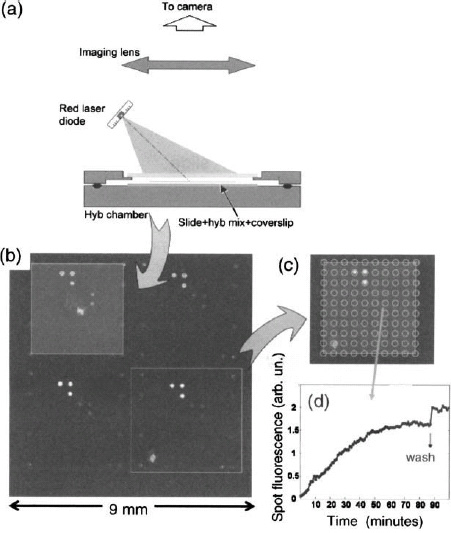
Figure 8. Real-time imaging of a microarray slide during hybridization. (a) Set-up using a fluorescence-enhancing slide; (b) fluorescence images at t = 16 minutes on Genewave’s AmpliSlideTM after background subtraction; (c) grid for analysis superimposed on bottom right block (L-shaped triplets within each block show PCR products hybridization, the spot intensities match their initial concentration in the mix); (d) spot fluorescence vs. time for the weaker spots of (c). Signal minus background increases linearly and then saturates at t ~ 60 minutes; washing, at 90 minutes, decreases significantly the background causing an apparent rise in signal.
Of course, one still observes significant background fluorescence due to the unbound fluorophores of the solution. It can be suppressed by washing the hybridization chamber, yielding images with a very high contrast ratio – see Fig. 8(d). Other schemes can increase the bound-to-free fluorophore contrast during hybridization, such as the use of evanescent wave excitation or spatially modulated amplification slides. The former scheme relies on the fact that exciting with a waveguided light beam will only excite those molecules within the evanescent part of the wave, i.e. those attached to the surface, together with only a very small fraction of those in the solution.11 Several ways of producing such waveguided modes are possible, such as coupling in a laser beam from the outside or using fluorescent species embedded in the waveguide. The spatial modulation scheme relies on an in-plane structuring of the amplifying slide, such that the amplification coefficient is spatially modulated between zero and maximum gain, preferably on a smaller scale than the spot size (one way to do it is to modulate the top layer thickness to obtain constructive or destructive interference). In that case, while the background fluorescence of the solution is constant over the slide, the signal originating from bound species is spatially modulated, so its demodulation and detection can recover a signal with enhanced dynamic range.
![]() The future
The future
There are other ways to further improve the sensitivity of microarray slides. One avenue is to improve the signal to noise per hybridization event. One can try to increase the fluorescence per event (by using fluorophores with larger excitation cross sections and higher fluorescence yield, such as quantum dots, molecular clusters, dendrimers, etc.) or suppress the fluorescence background (evanescent wave excitation, better molecular recognition schemes, such as molecular beacons or hairpin probes leading to less non-specific binding, etc.). Figure 9 shows a scheme where one uses a slide with a metal mask: in the imaging mode, the surface and volume generating spurious signals can be made extremely small by going with a small hole size. Further refinements can include other local techniques, like electrophoresis, to drive DNA to detection regions, opening the way to the detection of a single molecule hybridization.
It has been shown12 that deep-submicron holes actually enhance fluorescence due to surface plasmon enhancement. Such metal-masked system would achieve spatial filtering of background fluorescence in the object plane. The equivalent operation in the image plane, which is usually done in a confocal microscope on a single spot, is more difficult because it requires exact alignment of the filtering mask with the image.
5. Fluorescent biochips II: Integrated microarray and imaging systems
Contrary to the approach of increasing the efficiency fluorescence systems by diminishing emission towards the substrate, another approach relies on the fact that most of the light generated at an interface is emitted into the higher index material. A remarkable opportunity arises when using an imaging semiconductor integrated circuit, CCD or CMOS-based, as the substrate for the microarray. Then, the collection efficiency can be as high as 60-70% (all the light that is emitted downwards–see Fig. 7(a)) and no optical imaging of the spot is required, provided the spots are located close enough to the pixels: in a typical geometry, spots are 100 μm wide, distance between spot and pixel is a few microns, and pixel size is 5 15 μm. In that case, fluorescence from a given spot illuminates a few dozen pixels. Direct imaging of the spot is enabled by the proximity of the spot to the pixel and by the very small (undetectable) crosstalk between spots. Figure 10 shows the images obtained for a CCD imager directly spotted with fluorescent QDs (#QD800 dots from QD Corporation) at a concentration of 0.5 μM, observing the spots either directly from the CCD or imaging the spots on a similar CCD with wide aperture optics (NA = 0.5). The measured signal intensities differ by a factor of 30, as expected from the differences in collection efficiencies between the two geometries (> 60% for the integrated detection, ~2% for the imaging detection).
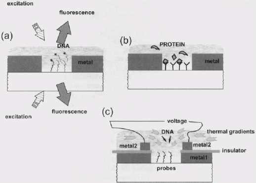
Figure 9. Hybridization detection can take advantage of localization by apertures in metal masks (a) for DNA detection by fluorescent labels; (b) for protein detection, with fluorescent tags or without; (c) with extra means (electrophoresis, thermophoresis, etc.), one can furthermore drive the DNA targets of other biomolecular targets towards the relatively tiny detection regions, increasing dramatically the rate of capture.
Of course this detection is made possible by the use of a high rejection, thin-film, wavelength-selective filter intcrcalated between the spots and the imager. Such a filter has to be integrated without a break in refractive index (i.e. without an air gap) in order to have the high collection efficiency due to the emission into a high index material. It also requires, as an order of magnitude calculation involving target fluorophore absorption cross sections easily shows, a wavelength-selective rejection ratio above 106 at all incidence angles.

Figure 10. Detection of fluorescent molecules directly spotted on a CCD camera through direct imaging on that camera: (a) principle of operation; (b) comparison with ordinary far-field fluorescence setup, using the same CCD; (c) far field image; (d) direct image, found to be 30x enhanced, i.e. harvesting 30 times more photons.
This cannot be achieved by a multilayer filter, but rather by using transition-metal dyes incorporated in a spin-on sol-gel matrix. The intrinsic fluorescence of this filter must low enough to observe the target fluorophore emission. The filter can either be deposited on the imager wafer or die, or be fabricated on a sacrificial substrate and bonded after fabrication on the imager, before or after chemical functionalization for probe attachment and/or probe spotting.
![]() The future
The future
Fabricating integrated hybridization-readout systems in standard silicon technology would integrate more functions in the device: the entire control and communication system can be integrated, with a USB interface to a computer. Full integration, with built-in biological tests, quality controls, and diagnostic software, will allow standalone biochip operation. In addition, more operations could be added thanks to the many opportunities provided by silicon technology, such as built-in electrodes for the fabrication of probes or high-efficiency hybridization thanks to electro-kinetic control of DNA or protein fragment motion. Further, the usual lab-on-chip functions can also be integrated. A schematic picture of such an integrated system is shown in Fig. 11.

Figure 11. Portable, sensitive and versatile biological detection system, integrated on a USB interface, focusing on the optical and data architecture (fluidic parts not shown). The light engine is integrated (side excitation) and the collected data from the array imager are partly treated on-board, and stored in a flash memory, together with the spotting information. This ensures perfect traceability and allows first-order analysis by an on-board processor. Full analysis is possible after transfer of raw or pre-treated data to a general-purpose computer.
6. Conclusions
High-efficiency emission collection strategies are central to both LED and microarray areas. For LEDs, while solutions appear to exist based on PC light extractors, industrial implementation faces stiff competition from schemes based on geometrical optics. Success will be more due to advantages in brightness and manufacturing performance than in raw extraction efficiency numbers.
For fluorescent microarrays, increased fluorescence collection efficiency not only can improve significantly the performance of biochips, but also allows new biodetection approaches. The integration of the hybridization and detection systems opens the way to fully integrated microarray bioanalysis systems with full automation: there have been many studies for the integration of the sample preparation (extraction and purification of DNA, RNA or proteins; biological amplification through PCR: hybridization) in the so-called lab-on-a-chip or micro total analysis systems. If these steps can be integrated with the detection systems, as described in this paper, they would lead to a fully integrated fluorescence detection scheme, which would be the most sensitive of all once proper light harvesting schemes are implemented.
Acknowledgments
The work on LEDs was supported in part by UC–Santa Barbara’s solid state lighting and display consortium (SSLDC), while the work on microarrays was supported in part by ANVAR, DGA and the E.U. project INDIGO.
References
- W. N. Carr, “Photometric figures of merit for semiconductor luminescent sources operating in spontaneous mode,” in: S.M. Sze, ed., Semiconductor Devices: Pioneering Papers, London: World Scientific, 1991, pp. 919–37.
- M. G. Craford, “Overview of device issues in high-brightness light-emitting diodes,” in: G. B. Stringfellow and M. G. Craford, eds., High-Brightness Light-Emitting Diodes, San Diego: Academic Press, 1997, pp. 47–64.
- M. Schena, Microarray Analysis, Hoboken, NJ: Wiley-Liss, 2003.
- H. Benisty, H. De Neve, and C. Weisbuch, “Impact of planar microcavity effects on light extraction—Part I: Basic concepts and analytical trends,” IEEE J. Quantum Electronics 34, 1612 (1998); “Impact of planar microcavity effects on light extraction—Part II: Selected exact simulations and role of photon recycling,” IEEE J. Quantum Electronics 34, 1632 (1998).
- C. Weisbuch, A. David, T. Fujii, et al., “Recent results and latest views on microcavity LEDs,” Proc, SPIE 5366, 1 (2004).
- M. Fujita, S. Takahashi, Y. Tanaka, T. Asano, and S. Noda, “Simultaneous inhibition and redistribution of spontaneous light emission in photonic crystals,” Science 308, 1296 (2005).
- A. David, C. Meier, R. Sharma, et al., “Photonic bands in two-dimensionally patterned multimode GaN waveguides for light extraction,” Appl. Phys. Lett. 87, 101107 (2005).
- A. David, T. Fujii, R. Sharma, et al., “Photonic-crystal GaN light-emitting diodes with tailored guided modes distribution,” Appl. Phys. Lett. 88, 061124 (2006).
- A. David, T. Fujii, B. Moran, S.Nakamura, S. P. DenBaars, C. Weisbuch, and H. Benisty, “Photonic crystal laser lift-off GaN light-emitting diodes,” Appl. Phys. Lett. 88, 133514 (2006).
- H. Choumane, N. Ha, C. Nelep, et al., “Double interference fluorescence enhancement from reflective slides: Application to bicolor microarrays,” Appl. Phys. Lett. 87, 031102 (2005).
- M. Pawlak, E. Grell, E. Schick, D. Anselmetti, and M. Ehrat, “Functional immobilization of biomembrane fragments on planar waveguides for the investigation of side-directed ligand binding by surface-confined fluorescence,” Faraday Discuss. 111, 273 (1998).
- H. Rigneault, J. Capoulade, J. Dintinger, et al., “Enhancement of single-molecule fluorescence detection in subwavelength apertures,” Phys. Rev. Lett. 95, 117401 (2005).