
Physical Limits of Silicon CMOS:
Real Showstopper or Wrong Problem?
CEA-LETI, 17 rue des Martyrs, 38054 Grenoble, France
1. Introduction
Digital information processing has become a key driver for the growth of the world economy. It has been fueled by the progress of microelectronics that is usually described by an exponential growth of some performance metric, often named Moore’s Law. Actually, the early papers of Gordon Moore1-3 only stressed the continuing search for a higher integration density of circuits, mostly through feature size reduction, while their electrical behavior was not even mentioned. It was not until the mid-1970’s that Robert Dennard formalized the benefits of downscaling device dimension:4 the present paradigm that miniaturization makes integrated circuits denser, faster, less power-hungry, cheaper and more reliable was born. The question then is how long will this trend last?
For more than two decades, technical papers announced the imminent dismissal of Si CMOS technology, stressing first the 1 μm barrier, then the 100 nm brick walls, and recently the 10 nm limit: to date they all proved to be wrong. After looking at some similar claims, we will focus on the so-called physical limits of the processing unit, trying to outline the underlying assumptions of such assertions and their possible shortcomings.
Assuming that classical Si CMOS will encounter some practical limits in the future, the latest version of the ITRS roadmap gives a thorough analysis of possible candidates for the “beyond CMOS” era. We will review the necessary criteria for a successful replacement of the Si CMOS gate for information processing and make a critical assessment of some of the proposed approaches.
However the real question is: are we looking at the right problem? The focus on logic gates may just be the tree hiding the forest of issues to be addressed in information processing. We should also consider major pending problems, like interconnecting those gates or manufacturing complex circuits useful for specific applications.
As a word of caution, this paper will restrict its analysis to digital processing units, leaving other semiconductor technologies, such as memories and analog devices, outside of the scope of this discussion.
2. A brief history of Si MOS limits
From the early days of microelectronics, an abundant literature explored the potential limits of the silicon technology: this chapter will mention a few milestones in this quest.
In the 1960’s and 197O’s, the focus was on the integration density – as exemplified by Moore’s paper1 – and the associated metric was the minimum achievable feature size. Among others, J. T. Wallmark published a detailed analysis of potential limits in shrinking dimensions5-7 and concluded that “the end of the road to smaller size has already been reached”8 – the smaller size being typically 5–10 microns in his early work. Pinpointing the flaws in his reasoning is not straightforward, but one can make a few remarks that may also apply to more recent papers on Si limits:
- the model of the elementary device is very crude (cube resistor, no signal restoration, etc.);
- the statistics used to assess circuit yield is questionable (e.g. cumulative independent events);
- some physical concepts (e.g. Heisenberg uncertainty principle) are misused.
In the 1980’s and 1990’s, the focus shifted towards speed and power consumption. Following these metrics, J. D. Meindl established a hierarchy of constraints in designing an integrated circuit:9
- at the most fundamental level, one faces physical limits dictated by quantum mechanics, thermodynamics and electromagnetism (i.e. relativity);
- more constraints are added when considering the materials used for fabricating the transistor, mostly associated with electrostatics (dielectric constant), carrier dynamics, thermal behavior and parameters fluctuations;
- the device architecture, the design style of the logic building blocks, and the system architecture and packaging bring additional constraints that limit considerably the design space in terms of power and delay.
However, considering the later levels of this hierarchy of constraints, as stressed by R. W. Keyes, “the potential tradeoffs [and the underlying assumptions] are too numerous and complex […] and they obscure the quantitative significance of [deriving] performance limits from purely physical reasoning”.10
The most recent works concentrate on the so-called “fundamental physical limits”. The general analysis is along the following lines11 (see Fig.1):
- thermodynamics (more specifically, the so-called “Landauer principle”12) suggests a minimum dissipated energy per operation, Emin ~ kBTIn2 ~ 17 meV at room temperature;
- from this minimum energy and from the first Heisenberg uncertainty relationship one derives a minimum device size, xmin ~ 1 nm;
- from the same minimum energy and from some time–energy relationship in a quantum system (using mostly the second Heisenberg uncertainty relationship) one deduces a minimum switching time, τ ~ 40 fs;
- these combined “limits” gives an upper value of the power density dissipated in a circuit whose transistors are packed at a maximum integration density and switch at the same time at the maximum speed. This estimate then gives a rather unrealistic ~4 MW/cm2 value of power consumption.
However, each step of this logical chain can and perhaps should be challenged. First of all, implicit assumptions related to the thermodynamic limit are numerous and potentially questionable, casting some doubt about the unavoidability of this barrier. Some of these questionable assumptions are made explicit below:
- the computing system interacts with its surroundings (e.g. thermal bath): computation is typically characterized by a relaxation time in most systems, but experimental work on quantum computing – among others – tends to indicate that some computation may be performed in a quasi-isolated system;
Figure 1. Combination of possible “fundamental physical limits” for a digital information processing mechanism. From the minimum switching energy Emin and from the Heisenberg uncertainty relationships, one derives the minimum size of the device xmin, and the minimum switching time τ, which translates into a maximum dissipated power per bit Pbit, and per area Pchip.
- information needs to be destroyed during computation (and its energy will be transferred to the thermal bath, i.e. dissipated): while this does happen in most of the present microelectronic circuits, reversible “adiabatic” computing13 aims to develop an alternative computing scheme where this statement does not apply. The applicability of such adiabatic computing to complex systems is still debated, however, as it is unclear if the associated energy benefit will outweigh the complexity overhead of a reversible computer;
- more fundamentally, the KBT In2 energy associated with a bit of information applies to a statistical ensemble of states in quasi-equilibrium: it has to be revisited for systems with few particles and states far from equilibrium (see, for example, Ref. 14).

Further, it should be noted that the first Heisenberg uncertainty relationship,
is used with the underlying assumption that the information carrier is localized. This imposes a much stronger constraint on the physical implementation of the computing mechanism than just assuming that the system should evolve among distinguishable (i.e. mutually orthogonal) quantum states. Furthermore many device models (see, for example, Ref. 11) assume a free quasi-particle as an information carrier in a quasi-static system, using a semi-classical approximation and without quantum confinement of the carrier: how far the resulting conclusions apply to a more realistic physical device needs to be explored. Finally, in these models Δx is loosely defined as the physical width of the energy barrier in the device and at the same time as the linear size of the transistor. A more rigorous discussion of the applicability of this limit in the most general instance of a physical computing device is still lacking.
The relationship between energy and time in a quantum system, using for example the so-called second Heisenberg uncertainty relationship,
is still more doubtful. Actually, two models may apply to the discussion:
- the classical interpretation15 of Eq.(2) states that in observing a quantum system during a time window Δt, the spread (i.e. standard deviation) in the measured energy of the system ΔE will be at least of the order of
 /2Δt. There is no clear reason to interpret ΔE as the energy dissipated during the transition between two distinguishable states, nor Δt as the transition time.
 - N. Margolus and L. Levitin derived another inequality16 giving an upper bound of the speed of evolution τ−1 of an isolated quantum system with respect to the average energy
 E
E of the orthogonal states of the system
- information needs to be destroyed during computation (and its energy will be transferred to the thermal bath, i.e. dissipated): while this does happen in most of the present microelectronic circuits, reversible “adiabatic” computing13 aims to develop an alternative computing scheme where this statement does not apply. The applicability of such adiabatic computing to complex systems is still debated, however, as it is unclear if the associated energy benefit will outweigh the complexity overhead of a reversible computer;
- more fundamentally, the kBT In2 energy associated with a bit of information applies to a statistical ensemble of states in quasi-equilibrium: it has to be revisited for systems with few particles and states far from equilibrium (see, for example, Ref. 14).
Further, it should be noted that the first Heisenberg uncertainty relationship,
![]()
is used with the underlying assumption that the information carrier is localized. This imposes a much stronger constraint on the physical implementation of the computing mechanism than just assuming that the system should evolve among distinguishable (i.e. mutually orthogonal) quantum states. Furthermore many device models (see, for example, Ref. 11) assume a free quasi-particle as an information carrier in a quasi-static system, using a semi-classical approximation and without quantum confinement of the carrier: how far the resulting conclusions apply to a more realistic physical device needs to be explored. Finally, in these models Δx is loosely defined as the physical width of the energy barrier in the device and at the same time as the linear size of the transistor. A more rigorous discussion of the applicability of this limit in the most general instance of a physical computing device is still lacking.
The relationship between energy and time in a quantum system, using for example the so-called second Heisenberg uncertainty relationship,
![]()
is still more doubtful. Actually, two models may apply to the discussion:
- the classical interpretation15 of Eq.(2) states that in observing a quantum system during a time window Δt, the spread (i.e. standard deviation) in the measured energy of the system ΔE will be at least of the order of /2Δt. There is no clear reason to interpret ΔE as the energy dissipated during the transition between two distinguishable states, nor Δt as the transition time.
- N. Margolus and L. Levitin derived another inequality16 giving an upper bound of the speed of evolution τ−1 of an isolated quantum system with respect to the average energy E of the orthogonal states of the system
![]()
Beside these explicit criteria the device is expected to have a number of implicit qualities. For example, the device should:
- operate at room temperature;
- perform order(s) of magnitude better than the Si CMOS “at the end of the roadmap”: no emerging device may expect to challenge the legacy of 40+ years of research, development and manufacturing of Si information processing systems if it does not offer significant advantages in some respect;
- be scalable, i.e. be applicable for more than just one or two technology generations, owing to the huge effort needed to displace Si CMOS;
- give a clear path for integrating other functions like memories, mixed-signal devices, and interface capability on the same chip;
- offer some perspective of mass-producing circuits at an affordable yield and cost (though it may be difficult to assess manufacturing issues at the very beginning of the research phase).
Unfortunately, according to the ITRS, no emerging logic devices21 passed the exam so far. In fact, many new devices have no chance of matching, even in the distant future, the integration density and/or speed of the CMOS technologies presently in production! On the other hand, one cannot exclude the discovery of a new structure or a revolutionary concept in the future.
One common pitfall of many disruptive device proposals is that, starting from an interesting physical effect for a unit information processing mechanism, it fails to show the capability to integrate complex functions in a way competitive with the present or future CMOS systems. Quantum-dot cellular automata (QCA, for short) provide an instructive example.
The concept of QCA was initially proposed by Tougaw, Lent and Porod22 in 1993. The basic idea relies on a bistable cell (e.g. quantum dots positioned at the 4 corners of a square and close enough to allow excess electrons to tunnel between neighboring dots) that appears to promise an extremely fast and low-power device. The equilibrium state (or polarization) of this cell depends on the states of the nearest-neighbor cells that are arranged in a way to map logic functions (e.g. majority gate) and allow signal propagation along a line. The computation is performed by forcing the states of the input cells at the periphery of the device and by letting the system relax to the ground state. The computation result is read out looking at the final state of the output cells at the periphery of the device. However, it became rapidly clear that this relaxation mechanism led to unpredictable computation time and possibly wrong results if the system got stuck into metastable states. This led to the need to implement a complex multiphase “adiabatic” (ie. slow) clocking scheme.23 A comparison of QCA with CMOS for logic blocks of small complexity concluded24 in 2001 that an ultimately scaled molecular QCA would barely compete with advanced CMOS in terms of operational frequency. Analyzing the achievable integration density would lead to the same conclusion. The application of QCA to complex circuits would also need more in-depth analysis of other potential issues:
- what is the actual power consumption of a clocked QCA, taking into account the power dissipated by the clock tree, and how it compares to standard CMOS for the same computational throughput?
- how scalable is the QCA approach?
- what is the noise immunity of the QCA scheme? Are there crosstalk issues and layout dependency?
- how manufacturing fluctuations will affect very complex systems?
- what is the set-up procedure of a complex QCA, i.e. how to control the exact number of excess electrons (or equivalent) in each of the hundreds of millions of QCA cells?
In short, after more than 12 years of research, QCA failed to provide a significant competitive advantage with respect to CMOS in terms of integration density, speed, power consumption, and implementation of complex systems. This interim conclusion has led to QCA using excess electrons in quantum dots and electrostatic interaction (so-called e-QCA) to be dropped from the list of potential emerging devices in the latest version of the ITRS. Surprisingly enough, magnetic and molecular variants of QCA did not share that fate despite facing the same basic issues.
Another, more subtle pitfall of many emerging devices and architectures lies in the difficulty of integrating the constraints of the whole chain from system architecture to complex circuits design, to manufacturing, test and assembly. In the recent years, there were many a ticles exploring the FPGA concept applied to nanoscale devices characterized by a very high fault rate. The basic idea25 resides in fabricating regular arrays of extremely miniaturized active devices, then in mapping the defects of the resulting structure, and finally in compiling and implementing the intended algorithm into the working elements. This potentially very attractive approach raises many questions, however.
- Rather than testing once a fixed design for its functionality and discarding the faulty devices, one needs to sequentially extract some defect map(s) of the chip, then compile the function into the working parts of the circuit and finally retest the implemented algorithm. In short, one trades off the yield issue of a potentially costly collective manufacturing with an expensive die per die multi-step functional test and programming. How far the efficiency of the test and programming algorithm may overcome the resulting increase in the test cost needs to be proven in realistically complex cases.
- Each of these “test & program” steps may lead to the impossibility to proceed further, e.g. too many defects may prevent further testing of the circuit if the test probe does not find any percolation path. A realistic yield model of this approach which would be compared with the yield of a more conventional random logic circuit having the same functionality is still lacking.
- It should also be noted that the proposed mesh-type structure of these nano-arrays may not be optimal in allowing the test of a significant part of the circuit: random and scale-free networks, such as the Internet, are known to be more resistant to random defects than a grid structure. This architectural aspect seems to be rather weakly addressed.
- Most of the nanoscale arrays rely on a diode-resistor type of logic. This design style was abandoned many years ago as it did not provide an easy method of signal restoration that was needed in the circuit (it does mean that a fine grained co-integration with restoring devices like CMOS is mandatory) and as functional gates were not cascadable. Added to that, one may expect a rather high static power consumption for complex circuits. How the new nanoscale crosspoint devices may address this architectural weakness has not been clearly discussed.
In conclusion, up to now all the emerging logic devices failed to show the capacity to be integrated into complex processing units. Part of the present situation may be attributed to the fact that the researchers who propose disruptive approaches are often marginally aware of the complexity of designing and manufacturing complex functions into an integrated system. Conversely, CMOS circuit developers are usually unable to explicitly enumerate all the criteria for a “good” device implemented into a “good” circuit architecture: convergence of both worlds is a challenge in itself.
4. Are we looking at the right problem?
The main focus of the major microelectronics conferences is the elementary processing unit (i.e. transistor or switch), the memories and their association into complex circuits.
More specifically, in the quest for higher performances, many publications look at different ways to increase the on-current ION of the transistor (or reduce the associated metrics CV/ION). Using the approximate formula,
![]()
where μ is the carrier mobility of the carrier, CG the gate capacitance and LG the physical gate length, one may infer three main directions in the progress of MOS transistors, enumerated below.
![]() Scaling of the critical LG dimension of the transistor
Scaling of the critical LG dimension of the transistor
This is the conventional way initiated by Dennard and others. However, in moving to smaller LG and in packing the different elements more closely together, unwanted interactions and parasitic effects become increasingly detrimental to the behavior of the classical planar MOS transistor. Alternative structures, like SOI, 3D fin-FETs, multiple-gate or multiple-channel devices, have been proposed for many years and in some limited cases are already implemented in production – e.g. SOI in some microprocessors. The rather slow technological insertion of these alternative architectures is not only related to the added processing complexity and its potential impact on yield. One should not forget that most of these “unconventional” MOS devices require a rethinking of the whole design flow of complex circuits, which is a major effort most companies cannot afford (even assuming the new technology significantly outperforms the traditional approach).
![]() Increasing the capacitive coupling CG of the gate and the conduction channel
Increasing the capacitive coupling CG of the gate and the conduction channel
The better electrostatic control of the conducting channel by the gate electrode was conventionally achieved by scaling the gate oxide thickness. Unfortunately, we reached dimensions where direct tunneling through the gate dielectrics leads to increasingly higher gate currents. To move away from this dead end, dielectrics with a high permittivity (the so-called high-κ materials) were proposed. However one cannot expect that the quasi-perfect Si-SiO2 system will be easily replaced: mobility degradation, Fermi level pinning and instabilities, among other drawbacks, are the present keywords of those high-κ dielectrics. As a result, these new materials are not expected to be introduced in the next CMOS generation.
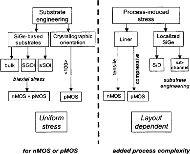
Figure 2. By applying different techniques for mechanically stressing the conductive channel and using different crystal orientations for the nMOS and pMOS, the carrier transport in the MOS transistors can be significantly enhanced.
As increasing transistor speed via traditional scaling becomes more and more difficult, enhanced transport of the carriers has been explored.
In the short term, the use of strain applied to the piezoresistive silicon and/or of other crystal orientations is a hot topic at device conferences. The combination of different techniques (see Fig. 2) allows balancing the benefits and drawbacks of each specific approach without adding too much complexity to the manufacturing process.
In the longer term, some researchers have proposed new channel materials to replace Si, such as Ge, III-V compound semiconductors, or carbon nanotubes. As in the case of high-κ dielectrics, one may expect significant processing difficulties and a diminishing return in the introduction of these materials into very complex integrated circuits.
The excitement about these “enhanced” MOS devices diverts attention from other equally important issues. In fact, one observes a widening gap between the research community and the real concerns of the microelectronics industry. The development engineer does not ask for breakthroughs in transistors and has more mundane questions, like:
- how can I use the same transistor architecture for high performance and low power applications and at different supply voltages?
- are adaptive power supplies, threshold voltages and clock frequencies applicable to the proposed technology?
- how does it allow input/output implementations?
- what will be the SRAM stability and its noise margin?
- is it possible to co-integrate digital logic, mixed signal circuitry and memories with the minimum increase in process complexity?
In fact, the present bulk planar MOS transistor provides legacy solutions even for the 45 nm technologies. As long as new transistor architectures do not answer all these questions related to their integration into complex circuits, they will remain “exotic” solutions for the future.
Interconnecting the processing units and memories in an efficient way is probably a more critical issue than building faster transistors: at this point, the wiring technology lags transistor performance. Optical interconnections, carbon nanotubes or even ultra-low-κ dielectrics are not expected to bring orders of magnitude improvement in performance requested by the transistor roadmap. Instead, further progress will likely require a wise combination of design techniques and advanced manufacturing.
The microelectronics is clearly at a turning point in its history.
- In the last decades, digital technology – and especially dimensional scaling – drove the progress of this industry, looking at a lower cost and a better performance per gate. As no disruptive breakthrough is presently in sight, the likely path is to stay with a Si CMOS-based logic, adding new materials and device architectures for enhancing the overall circuit performance. One may imagine a situation where downscaling will no longer serve as the right metric of progress in microelectronics technology (just as the speed of commercial aircraft is no longer the measure the progress in the aeronautics industry26).
- The value of the functions co-integrated on the same circuit will become an ever more powerful industry driver. This will call for a diversification of devices integrated on the same chip – a trend we might label “More than Moore”, – and of the associated technologies that do not necessarily scale with the dimensions. The perceived limits might well change qualitatively as the design space is redefined.
- At the end, the real value will be what is perceived by the end user – i.e. enhanced services, specific features, etc. – with the actual technology behind the application being of lesser importance. Added value through software and system design may play a preeminent role alongside pure technology, adding more degrees of freedom for further progress.
5. Conclusions
While the future of microelectronics is fuzzier than ever, it is too early to conclude that we are (almost) at the end of the road. Too many bright scientists predicted insurmountable limits and declared some physical implementations impossible, from airplanes to nuclear power, for us to be sure of the progress in Si logic is over. I would suggest applying a creative skepticism to any claim related to approaching limits, by clarifying all the underlying assumptions and trying to surmount or sidestep the obstacles.
Looking back to the past decades there is no reason to be pessimistic and it is safe to say that one cannot imagine what technology will be possible a few decades from now. On the other hand, it is also wise not to be too optimistic: the recent hype about new switches or new computational approaches may prove to be just hype. One should never underestimate the real complexity of building a working information processing technology and of replacing the accumulated knowledge and know-how of the present microelectronic industry by something totally new.
Acknowledgments
I would like to specifically thank Daniel Bois, Sorin Cristoloveanu, Hervé Fanet, Paolo Gargini, James Hutchby, Hiroshi Iwai, Thomas Skotnicki, Paul Solomon and Claude Weisbuch, who raised my interest in exploring the limits of Si CMOS and helped me (some of them unconsciously) to put this work together.
References
- G. E. Moore, “Cramming more components onto integrated circuits,” Electronics 38, 114 (1965); reproduced in Proc. IEEE 86, 82 (1998).
- G. E. Moore, “Progress in digital integrated electronics,” Tech. Digest IEDM (1975), pp.11–13.
- G. E. Moore, “Lithography and the future of Moore’s law,” Proc. SPIE 2437, 2 (1995).
- R. H. Dennard, F. H. Gaensslen, H.-N. Yu, V. L. Rideout, E. Bassous, and A. R. LeBlanc, “Design of ion-implanted MOSFETs with very small physical dimensions,” IEEE J. Solid-state Circ. 9, 256(1974).
- J. T. Wallmark, “Basic considerations in microelectronics,” chapter 2 in: E. Keonjian, ed., Microelectronics, New York: McGraw-Hill, 1963, pp. 10–96.
- J. T. Wallmark, “Fundamental physical limitations in integrated electronic circuits,” in: Solid State Devices 1974, Conf. Series No. 25, London: Institute of Physics, 1975, pp. 133–167.
- J. T. Wallmark, “A statistical model for determining the minimum size in integrated circuits,” IEEE Trans. Electron Dev. 26, 135 (1979).
- J. T. Wallmark and S. M. Marcus, “Maximum packing density and minimum size of semiconductor devices,” IRE Trans. Electron Dev. 9, 111 (1962).
- J. D. Meindl, Q. Chen, and J. A. Davis, “Limits on silicon nanoelectronics for terascale integration,” Science 293, 2044 (2001).
- R. W. Keyes, “Physical problems and limits in computer logic,” IEEE Spectrum 6, 36 (1969)
- V. V. Zhirnov, R. K. Cavin, J. A. Hutchby, and G. I. Bourianoff, “Limits to binary logic switch scaling – a gedanken model,” Proc. IEEE 91, 1934 (2003).
- R. Landauer, “Irreversibility and heat generation in the computing process,” IBM J. Res. Develop. 5, 183 (1961).
- M. P. Frank and T. F. Knight, Jr., “Ultimate theoretical models of nano-computers,” Nanotechnology 9, 162 (1998).
- J. Casas-Vásquez and D. Jou, “Temperature in non-equilibrium states: A review of open problems and current proposals,” Rep. Prog. Phys. 66, 1937 (2003).
- L. I. Mandelstam and I. E. Tamm, “The uncertainty relation between energy and time in non-relativistic quantum mechanics,” J. Phys. (USSR) 9, 249 (1945).
- N. Margolus and L. B. Levitin, “The maximum speed of dynamical evolution,” Physica D 120, 188 (1998).
- I implicitly exclude the fundamental work of A. Turing and others, particularly Turing’s halting problem, that brought Gödel’s theorem into the computer field: the practical limitation it imposes on actual computing schemes is, however, not obvious.
- R. W. Keyes, “Physics of digital devices,” Rev. Mod. Phys. 61, 279 (1989).
- R. W. Keyes, “The cloudy crystal ball: Electronic devices for logic,” Phil. Mag. B 81, 1315 (2001).
- The International Technology Roadmap for Semiconductors: 2005 Edition – Emerging Research Devices. This document can be downloaded from http://www.itrs.net/Links/2005ITRS/ERD2005.pdf
- I exclude ID FETs that do not offer any conceptual breakthrough and are merely aggressively scaled MOS transistors potentially using an alternative channel material (Ge, III-V or carbon nanotube).
- P. D. Tougaw, C. S. Lent, and W. Porod, “Bistable saturation in coupled quantum-dot cells,” J. Appl. Phys. 74, 3558 (1993).
- C. S. Lent and P. D. Tougaw, “A device architecture for computing with quantum dots,” Proc. IEEE 85, 541 (1997).
- K Nikolić, D Berzon, and M. Forshaw, “Relative performance of three nanoscale devices – CMOS, RTDs and QCAs – against a standard computing task,” Nanotechnology 12, 38 (2001).
- A. DeHon and K. K. Likharev, “Hybrid CMOS/nanoelectronic digital circuits: Devices, architectures, and design automation,” Proc. ICCAD 2005, pp. 375–382.
- H. Iwai, “Recent advances and future trends of ULSI technologies,” Tech. Digest ESSDERC (1996), pp. 46–52.