
Absolute Negative Resistance in Ballistic Variable Threshold Field Effect Transistor
Laboratoire de Physique Théorique et Astroparticules
Université Montpellier II, France
ECSE Department and Broadband Center
Rensselaer Polytechnic Institute, Troy, NY 12180, U.S.A.
We consider a ballistic variable threshold field effect transistor (BVTFET),1-4 where the electron transport is ballistic (no collisions with impurities or lattice vibrations), see Fig. 1(a). We will use the hydrodynamic approach,5 which is justified if the electron-electron collisions are much faster than collisions with impurities andlor phonons. Qualitatively, our results hold even if this condition is not met, so long as the mean free path is greater than the characteristic length scale for the variation of the electron concentration.
Within this approach, the situation we consider is similar to a water flow through a pipe with varying cross-section, see Fig. l(b) and (c). If there is no flow, obviously the pressure is the same on both sides. In the presence of a stationary water flow, the Bernoulli law (which follows from energy conservation) tells us that the pressure will be lower in the narrow part of the pipe, where the velocity is larger. Note, that this fact does not depend on the direction of the flow. This means that when water flows from the narrow part towards the wide part, the direction of the flow is locally opposite to the pressure gradient. One can say that the interface region has an absolute negative resistance. We will show below, that a similar effect should exist for the BVTFET.
To be specific, we assume, as shown in Figure 1, that the device threshold voltages for the section with coordinates 0 < x < L1, and L1 < x < L are VT1 and VT2, respectively (with VT2 < VT1) and that the source contact at x = 0 is grounded. The gate and drain voltages are VG and VD, respectively. The voltage drop in the ballistic sections of the device is zero, so the entire voltage drop occurs at the interface between the two sections at x = L1 , see Fig. 1(a). We will treat this interface as abrupt, assuming that the Debye length and the separation between the gate and the channel are small compared to L1.
The basic equations describing this device are the equation of motion and the continuity equation,
as well as the equations relating the concentrations n to the local gate-to-channel voltage swing in the gradual channel approximation:
Here C is the gate-to-channel capacitance, e is the electron charge, VG is the gate voltage, VT1 and VT2 are the threshold voltages for the left and right sides of the transistor respectively, VD = V1 − V2 is the source-drain potential difference, V1 and V2 are the channel potentials on the left and on the right side of the device.
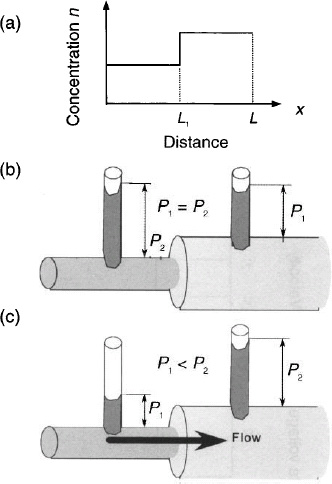
Figure 1. (a) Electron concentration distribution in a variable threshold field effect transistor; (b) a water pipe with varying cross section. In the absence of flow the pressures on both sides are obviously equal; (c) the same water pipe in the presence of flow – the pressure in the narrow part of the pipe is lower (Bernoulli law), regardless of the flow direction.
In the stationary situation that we are considering, Eqs. (la) and (1b) yield:
where v1 and v2 are the left and right electron drift velocities, The first of Eqs. (4) is analogous to the Bernoulli law in hydrodynamics.
We denote by n10 and n20 the equilibrium electron concentration on the two sides of the interface when the current is absent. The concentration. velocity, and gate voltage swing profiles for the case n10 < n20 are shown in Fig. 2. We will be interested also in the opposite case, when n10 > n20. We will consider the situation when the left side of the device with the electron concentration n10 is grounded (V1 = 0). Then the concentration on this side is always fixed: n1= n10. while the concentration on the right side, n2, will vary with changing current.
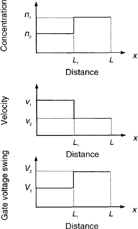
Figure 2. Concentration, velocity, and gate voltage swing profiles in BVTFET for the case n10 < n20. Obvious modifications should be made for the opposite case.
If n10 < n20 and v1 > v2 (see Figure 2), VD is negative (meaning that the high concentration side has a more negative potential than the low concentration side with the electron concentration n1). In the opposite case, when n10 > n20 and v1 < v2, VD is positive.
We now introduce dimensionless variables U for the source-drain voltage and J for the current, together with a dimensionless parameter N defined as the ratio of the carrier concentrations in the right section of the device to that in the left section in equilibrium (i.e. at zero current):
U ≡ C|VD|/enl0, J ≡ V1/V0, N ≡ n20/n10 = 1 + C(VT1 – VT2)/en10,
where the characteristic electron velocity v0 is given by:
![]()
We find from Eqs. (2)–(4) for negative VD:
and for positive VD, respectively:
For typical values of an AIGaAs/GaAs ballistic HEMT, we can assume VG = 0, VT2 = −1 V, VT1, = −0.5 V, m = 0.067m0 (where m0 is the free electron mass), and C = 5×10⁻⁷ F/cm2 (corresponding to approximately 20 nm gate-to-channel separation). These values yield a characteristic current density of approximately 4 μA/μm.
In the dimensionless units introduced above, Eqs. (5) and (6) can be rewritten as:

For N > 1 (i.e. n10 > n20), VD is negative and increases the carrier concentration in the high-concentration section of the device. As seen from Eq. (7a), for N > 1 at large U, J2 is proportional to U. At small U << N, the current-voltage characteristic for both cases becomes:
Since typical current densities achieved in AIGaAs/GaAs HEMTs correspond to the range of J between 0.01 and 0.2, in many cases, Eq. (8) should apply.

Figure 3. Dimensionless current-voltage characteristics of BVTFET for N = 1.01, 1.1, 1.6, and 10 plotted on linear (top) and double log (bottom) scales.
The resulting current-voltage characteristics for are shown in Fig. 3. For n10 < n20, the carrier concentration in the right section of the device increases proportionally to the absolute value of VD, as seen from Eq. 6(a). The dimensionless electron velocity in this section is given by
For n10 < n20, velocity v2 reaches a maximuin value at:
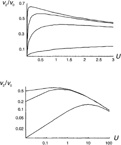
Figure 4. Dependence of v2/v0 on U for N = 1.01, 1.l, 1.6 and 10 plotted on linear (top) and double log (bottom) scales.
Figures 4(a) and 4b show the dependence of v2/v0 on U for n10 < n20. In the opposite bias polarity, when n10 > n20, we have N < 1 and VD is positive. The resulting current-voltage characteristics for n10 > n20 obtained from Eq. (7b) are shown in Fig. 5, where we also superimpose the dependence of the choking current JCH on the choking voltage UCH (found from the requirement that the electron velocity in region 2 for n10 > n20, N < 1 is equal to the plasma wave velocity in this region)6
As can be seen, the maxima of the current-voltage characteristics at N > 0.75 correspond to the choking current.

Figure 5. Dimensionless current-voltage characteristics of BVTFET for n10 > n20 and N = 0.5, 0.75 and 0.99 plotted on linear (a) and double log (b) scales. The choking current dependence on the choking voltage is also shown.
Figure 6 shows the dimensionless electron velocity in region 2 as a function of U for N < 1, where we also superimpose the dependence of the choking velocity on the choking voltage (found from the requirement that the electron velocity in region 2 for nl0 > n20, N < 1 is equal to the plasma wave velocity in this region):
The physical meaning of the obtained results is as follows. The electrons crossing the boundary at x = L1 must keep their energy. which can be only achieved by creating a dipole layer at the boundary leading to the voltage drop that changes the electron concentration in one section of the device and adjusts the electron velocities in both device sections accordingly. In the device section with the fixed potential, the carrier concentration is independent of the current. The other section accommodates any change in current by adjusting the carrier concentration. If the concentration in this section is higher, it increases further with an increase in the device current. If the concentration in this section is smaller, it gets depleted with an increase in the device current. The striking result is that this voltage drop is independent of the direction of the current, so that, depending on the direction of the current, the device should exhibit equal positive or absolute negative resistance. The consequences of this absolute negative resistance will be discussed elsewhere.

Figure 6. Dimensionless velocity v2/v0 in section 2 for n10 > n20, for N = 0.5, 0.75 and 0.99 vs. U. The choking velocity dependence on the choking voltage is also shown.
Acknowledgments
This work was supported in part by ONR under EMMA MURI contract (project manager Dr. Colin Wood).
References
- M. S. Shur, “Split-gate field effect transistor,” U.S. patents 5,012,315 (April 30, 1991) and 5,079,620 (January 7, 1992).
- G. Kelner and M. S. Shur, “Junction field effect transistor with lateral gate voltage swing (GVS-JFET),” U.S. patent 5,309,007 (May, 1994).
- M. S. Shur, “Split-gate field effect transistor,” Appl. Phys. Lett. 54, 162 (1989).
- G. U. Jensen and M. S. Shur, “Variable threshold heterostructure FET studied by Monte Carlo simulation,” in: K. Hess, J. P. Leburton, and U. Ravaioli, eds., Computational Electronics. Semiconductor Transport and Device Simulation, Norvell, MA: Kluwer Academic Publishers, 1991, pp. 123–6.
- M. Dyakonov and M. S. Shur, “Shallow water analogy for a ballistic field effect transistor. New mechanism of plasma wave generation by dc current,” Phys. Rev. Lett. 71, 2465 (1993).
- M. Dyakonov and M. S. Shur, “Choking of electron flow – A mechanism of current saturation in field effect transistors,” Phys. Rev. B 51, 14341 (1995).