
Scaling Limits of Silicon CMOS and Non-Silicon Opportunities
Dept. of Electrical Engineering, Stanford University, Stanford, CA 94305, U.S.A.
1. Introduction
As we look at the future of silicon based CMOS, it is becoming more difficult to be as optimistic as we used to be. A variety of problematic issues and, more importantly, the magnitude of anticipated challenges, may not be as easy to circumvent as those we have successfully overcome over the past two decades. Not only difficulties in cost-effective processing equipment and process parameter controls, but also perceived limits in device operation improvement itself will pose more problems than in the past. Rapidly increasing MOSFET leakage currents at the gate, source, and drain terminals, and the diminishing improvement in the drive current with reduced channel length are now pushing us to consider alternative materials for the channel of MOSFETs. At the integration level, the interconnect delay that has been identified as the stumbling block for large high-performance chips will certainly become worse, coupled with power consumption and heat dissipation management challenges. As we will have more areas dedicated to high-speed embedded memory, mostly consisting of static random access memory (SRAM), memory standby power will become a major problem, especially with MOSFETs operated at a much lower ION/IOFF ratio than they used to be. Furthermore, general trends for system-on-a-chip design driven by significant growth of wireless systems, mostly for consumer products, will require heterogeneous integration of digital, analog/RF, power management and more, which will make the magnitude of challenges greater than ever.
This chapter will discuss present and future perspectives of nanoelectronic materials and devices both in evolutionary and revolutionary “nano” electronics domains. It is likely that the evolutionary progress in all problem areas of silicon-based CMOS will keep its pace, despite a variety of technical challenges. Revolutionary nanoelectronics, such as nanowires and nanotubes, could provide unique advantages, but only when engineering breakthroughs for control of growth, placement, and integration are achieved.
2. Silicon-based CMOS scaling
“Scaling” has provided continuous improvement of digital integrated circuits (ICs) through cost reduction per bit/gate combined with improved current drive without an increase in the leakage current. This has permitted the semiconductor industry to stay with the same material, silicon, and ensured evolutionary progress of processing equipment with continuous productivity improvement. However, as illustrated in Fig. 1, we are coming to the juncture at which scaling may cease to provide the necessary performance improvement. It is evident from Fig. 1 that the scaling-driven current drive improvement is saturating, while subthreshold current leakage as well as band-to-band tunneling leakage at the drain junction edge are both increasing. Furthermore, the fundamental tool for geometry scaling, photolithography, is facing its greatest challenges ever. Not only a variety of resolution enhancement techniques, but a hardware revolution involving liquid immersion lithography and extreme UV sources will be needed soon, with many issues to be solved before practical utilization. Finally, one-dimensional silicon scaling for digital ICs is giving way to multi-functional integration with digital, ananlog/rf, power management, non-volatile memories, and even MEMS with 2D and 3D configurations.
Of course, much ongoing research continues to be invested in overcoming the obstacles to the continued growth of integration density. They can be classified into four areas, as shown in Table 1. Improvement in electrostatic control of field-effect devices has fostered interest in new structures that promise better control over the channel current flow, such as double gate, fin-FET, ultra-thin body (UTB) SOI, and metal gate devices. Combinations of metal gates and high-κ dielectrics, shown in Table 2, have been aggressively pursued, leading to a large number of publications, but it appears more effort will be needed before these technologies will hit the manufacturing floor.

Figure 1. Saturating trends of MOSFET performance improvement with scaling: (a) current drive ION vs. gate length at constant IOFF (data from IBM, TI, Intel, AMD, Motorola and Lucent);1 (b) contrasting requirements for high ION ~ (VDD − VT)η provided by low VT and low IOFF provided by high VT.
Table 1. Possible alternative materials and structures for future MOSFETs.

As for the transport in the channel, a couple of approaches for the energy band engineering have been studied, using both strain and quantum confinement. Also, new materials that have higher electron and/or hole mobilities have been explored, resulting in Ge and III-V compound semiconductor channel MOSFETs. Finally, source-drain leakage mechanisms, including drain-substrate leakage, have become hot topics. Recently, more attention has been paid to source resistance, as the source/drain junction depth is getting smaller in order to reduce drain-induced barrier lowering (DIBL) and short channel effects, There is now increasing research into metal source/drain structures.2
Taking a closer look at band engineering of silicon n-MOSFETs for better electron mobility, the leading approaches involve biaxial or uniaxial tensile strain on (100) surface or making channel thickness enough small as compared to the electron wave function spread, e.g. ultra-thin body UTB-SOI.3 Both of these techniques split the six constant energy conduction band ellipsoids into 2-fold and 4-fold degenerate ellipsoids, and the preferentially populated 2-fold ellipsoids with lighter transport mass mT* enhance the mobility. Compressive strain, on the other hand, makes the conductivity effective mass of holes smaller, thereby improving the p-MOSFET.
A number of technological procedures for such band engineering have been proposed and are now in production, especially the use of silicon nitride as a uniaxial strain-generating film for n-channel and SiGe heterostructure source and drain for p-channel. Research into using high-mobility III-V compound semiconductor channels is now on its way. As shown in Fig. 2, this approach is attractive because most of III-V materials have significantly higher electron mobility than silicon. However, when the high mobility is based upon low effective mass of electrons, the density of states is also low, and the drain current – the product of mobility and carrier concentration may not be as high as one might expect from the mobility improvement alone.
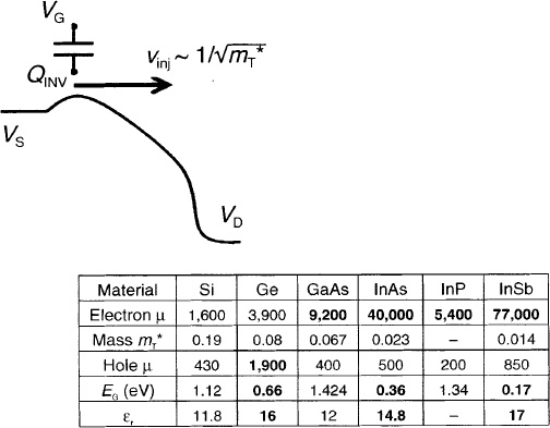
Figure 2. Possible high-mobility channel materials. Note that low EG, increases leakage due to band-to-band tunneling, while high εr increases short-channel effects.
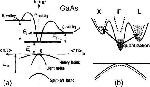
Figure 3. (a) GaAs bulk band diagram, showing the three conduction band valleys; (b) schematic illustration of electron spillover from high mobility Г valley to lower mobility X and L valleys due to quantum confinement.4
Figure 3 shows the band diagram of GaAs and a schematic example of a quantum-confined GaAs band structure in which the Г valley is pushed up to higher energy and electrons in that valley spill out to X and L valleys.4 This increases the contribution of X and L valley electrons to the overall channel conduction, but the mobility of X and L valley electrons is much lower. The same type of intervalley transfer in quantum-confined channels can happen in other channel materials.
If alternative III-V channel materials can achieve higher electron mobility than strained silicon for n-MOSFETs, the next challenge would be to do the same for p-MOSFETs, because the hole mobilities in III-V materials are no higher than in silicon. This is perhaps where Ge channels could play a major role. The challenge for Ge channel devices is both control of the interface to high-κ dielectrics and also that narrow Ge bandgap that can cause undesirable pn junction leakage and band-to-band tunneling at the drain edge. In order to cope with these issues, hetero-structured channel devices have been proposed and verified by both simulation and experiments.5 Generally speaking, we certainly need much more experimental data to further investigate these new material-based options. In the case of III-V semiconductors, in particular, technological promise requires the bold assumption that we can achieve highly controlled III-V semiconductor-insulator interfaces.
3. Nanoelectronic materials and devices
There are a number of opportunities on the horizon beyond silicon CMOS scaling. There are many attractive candidates such as carbon nanotube devices, nanowire devices, molecular/organic devices and spintronic devices. Both carbon nanotubes and semiconductor nanowires have been extensively studied already, and have exhibited promising electrical characteristics. Figure 4 shows an example of carbon nanotube MOSFET with Schottky source and drain electrodes.6
However, at this moment the biggest challenge for both nanotubes and nanowires lies not in the device characteristics, but rather in achieving highly controlled growth of tubes and wires at specified locations. The growth of semiconducting single-wall carbon nanotubes with anything near 100% yield has not been established. Also nanotube-specific characteristics, such as ambipolar conduction, present a number of design challenges if and when nanotubes reach the stage of practical deployment in ULSI circuits of the future.
Another important area outside of high-performance switching devices is nonvolatile memory. A number of nonvolatile memory technologies based on phase change, resistance change, dielectric polarization, magnetic polarization and nanoparticle floating gate devices have been attracting attention. Molecular/organic memories may eventually be added to this list.
Both ferroelectric and phase-change memories have a long research history since the pioneering original demonstrations, but are only now finally reaching technological insertion as high density embedded nonvolatile memory, standalone nonvolatile memory, and possibly even nonvolatile logic elements. The conductance bridge memory is another example of an emerging “nano” memory. Switching characteristics of the conductance bridge memory are shown in Fig. 5,7 where on-resistance is set by nanofilamentary conduction and is area independent, whereas off-resistance is determined by electronic conduction across the memory material and depends on area – scaling of such memory actually improves the on/off ratio, which is a promising feature.

Figure 4. Complementary carbon nanotube MOSFETs.
Figure 5. Conductance bridge memory characteristics.7
4. Three-dimensional (3D) integration
Despite a number of trials, the practical realization of 3D circuits has proven difficult because everything we have developed over the past four decades was focused on 2D integration, i.e. design tools, circuits testing, failure diagnostics, and, of course, the scaling paradigm itself. Today we are finally beginning to see a rudimentary shift towards 3D integration, but only at the packaging level. The fundamental advantages of true 3D integration are many, including the reduction of the chip footprint, the minimization of interconnect length and hence minimization of interconnect R, L, C which would reduce power consumption and delay, and possible integration of heterogeneous technologies, such as logic, memory, sensors, I/O’s and even MEMS. Recent progress toward monolithic integration has been achieved by using either wafer stacking or monolithic stacking as shown in Fig. 6 for the case of Ge single-crystal recrystallization in vias on top of silicon.

Figure 6. Germanium-on-insulator film by rapid melt growth.8
Unfortunately, true 3D monolithic integration appears unlikely in the foreseeable future. However, if such integration did arrive, one of the most promising areas of application would be in FPGAs. Furthermore, heterogeneous material combinations, such as a silicon-based CMOS platform coupled with Ge-channel MOSFETs or similar combinations with other materials, could become possible, as in Fig. 6. Such 3D integration could become a cornerstone technology for integrating multifunctional capabilities on a single chip, though testability, redundancy, reliability and manufacturing cost issues remain areas for future research and development.
5. Summary
As we look at available and/or soon-to-be available technologies from a practical viewpoint, there is no doubt that we still have a lot of room to explore before departing from silicon-based CMOS by expanding to new materials and device structures, and new ways to design and test chips. There is hope that the world of “nano” will keep providing revolutionary/evolutionary solutions that would significantly benefit our society directly or indirectly.
References
- C. Choi, “Modeling of nanoscale MOSFETS,” PhD thesis, Stanford University (2002).
- For example, J. Larson and J.P. Snyder, “Overview and status of metal S/D Schottky-barrier MOSFET technology,” IEEE Trans. Electron Dev. 53, 1048 (2006).
- K. Uchida, T. Krishnamohan, K. Saraswat, and Y. Nishi, “Physical mechanisms of electron mobility enhancement in uniaxial stressed MOSFETs and impact of uniaxial stress engineering in ballistic regime,” Tech. Digest IEDM (2005), pp. 135–8.
- A. Pethe, T. Krishnamohan, D. Kim, S. Oh, H. S. P. Wong, Y. Nishi, and K. Saraswat, “Investigation of the performance limits of III-V double-gate n-MOSFETs,” Tech. Digest IEDM (2005), p. 619.
- T. Krishnamohan, Z. Krivokapic, K. Uchida, Y. Nishi, and K. Saraswat, “High mobility ultrathin strained Ge MOSFETs on bulk and SOI with low band-to-band tunneling leakage: Experiments,” IEEE Trans Electron Dev. 53, 990 (2006).
- A. Javey, J. Guo, Q. Wang, M. Lundstrom, and H. Dai, “Ballistic carbon nanotube field effect transistors,” Nature 424, 6949 (2003).
- Z. Wang, P. B. Griffin, J. McVittie, S. Wong, P. C. McIntyre, and Y. Nishi, “Resistive switching mechanism in ZnxCd1-xS nonvolatile memory devices,” to appear in IEEE Electron Dev. Lett. (2007).
- Y. Lu, M. D. Deal, and J. D. Plummer, “High quality single-crystal Ge-on-insulator by liquid-phase epitaxy on Si substrate,” Appl. Phys. Lett. 84, 2563 (2004).