Intersubband Quantum-Box Lasers: An Update
Reed Center for Photonics, University of Wisconsin, Madison, WI 53706, U.S.A.
University of Florida, Gainesville, FL 32611, U.S.A.
1. Introduction
Semiconductor lasers operating continuous wave (cw) at or near room temperature (RT) and emitting in the mid- and far-infrared wavelength ranges, 3–13 μm, are critically needed for a vast array of applications. Intersubband (IS) transition emitters are the most likely solution. The first implementation of the concept for using IS transitions for laser action,1 was realized in early 19942 and named the quantum cascade (QC) laser. Current QC devices have demonstrated room-temperature cw operation at 4.3 μm and 4.8 μm,3,4 but with very low wallplug-efficiency values (< 2.5%) due to inherently high operating voltages (10–11 V). Furthermore, these devices have extremely temperature-sensitive characteristics3,4 at and near RT, due to thermal runaway triggered by the backfilling effect,5,6 which raises serious issues of device reliability. In fact, no device reliability has been demonstrated to date for any type of QC laser.
Intersubband-QC lasers have fundamentally poor radiative efficiencies since the nonradiative, LO-phonon-assisted relaxation time for electrons in the upper laser states is about 1.8 ps,5 whereas the radiative relaxation time is 4.2 ns. That is, nonradiative processes are about 2300 times faster than radiative processes. Since there are good reasons to believe that the LO-phonon-assisted relaxation time will substantially increase if the relaxing electrons are confined in quantum boxes7-16 the radiative efficiency problem can be overcome by replacing the quantum-well (QW) active regions of a QC laser with a quantum-box (QB) 2D array6,17 or a 2D array of cascaded QBs.18
2. Intersubband quantum box lasers
In QW structures electron relaxation between subbands occurs2,5 in about 1–2 ps, primarily via LO-phonon absorption or emission.5,7 Making QBs causes discrete states in the subbands,6,17 which in turn causes the LO-phonon-assisted electron relaxation time to increase7,9 by a factor β.6 Experimental results10-14 from unipolar QBs (where electron-hole scattering10 does not circumvent the phonon bottleneck) and photocurrent-response/dark-current measurements from QB IR detectors11,15 indicate electron-relaxation times of the order of 100 ps, in good agreement with theory.16 As the temperature increases to RT the relaxation times decrease12,13 due to inherent carrier losses from self-assembled QBs to the wetting layers.19 The proposed QBs are not self-assembled and thus can be made deep, resulting in negligible carrier leakage with increasing temperature. Therefore, for deep InGaAs/GaAs QBs β may well be as high as 50 at RT. zBased on the experiments in Refs. 10–14, we feel confident to assume that for deep QBs β > 30.
The proposed device is schematically shown in Fig. 1: an intersubband-transition laser with an active region composed of a 2D array of QB ministacks, called “active boxes”, separated by current-blocking material (CBM). Each mini-stack is composed of 2 to 3 QBs. The QBs will be fabricated by in-situ gas etching and regrowth, allowing for tight carrier confinement, unlike the inherently weak carrier confinement of self-assembled QBs. The active-boxes array, together with lightly doped n-GaAs layers constitute the core of an optical waveguide with heavily doped n+-GaAs cladding layers. A standard four-level laser theory has been used by us6 to estimate the threshold-current density JTH, differential quantum efficiency ηD, and the wallplug efficiency ηP, of IQB and QC lasers (λ = 4.5 μm). We obtained ηP values of 24% at RT for single-stage IQB devices; that is at least an order of magnitude higher than for conventional QC devices3,4 emitting in the 4.0–4.8 μm range.

Figure 1. Representation of the intersubband quantum box structure, where CBM denotes current blocking material.

Figure 2. Schematic representation of a QB ministack (i.e. active boxes) and the conduction-band energy diagram inside one QB (λ = 4.8 μm).
To achieve enough gain for higher wallplug efficiencies (larger than 25%) one requires ministacks of QBs: 2-3 in a vertical row, each of which having the conduction-band energy diagram shown in Fig. 2. The active region has two deep wells,20 resulting in a high energy barrier for electrons in the upper energy state E3 (~300 meV in Fig. 2) that suppresses thermionic carrier leakage. Furthermore, unlike QC lasers, the injector and Bragg mirror regions are separate, which ensures the suppression of carrier backfilling in multi-stage devices. The design of Fig. 2 incorporates a strain-compensated structure using tensile-strained GaAsl-xPx layers to prevent defect formation due to strain relaxation21 during the etch and regrowth process.
Let us now consider a 2D array of double QB stacks. A transverse waveguide of low loss coefficient αW = 1.5 cm-1 has been designed. Then, for 2 mm-long, 10μm-aperture devices with 10% and 90% front- and back-facet reflectivities and taking β = 30, the calculated cw wallplug efficiency ηP at RT reaches a maximum of 50.3% at J ~ 6JTH, see Fig. 3. If β = 50, ηP reaches a maximum of 54% at ~8JTH. For the cw ηP calculations, we took a series resistance of 0.16 Ω consistent with a comprehensive study of QC devices,22 and a thermal resistance RT = 1.5 K/W, also consistent with measurements in QC devices22 as well as the fact that bulk material has an RT value at least a factor of five times smaller than that for thick superlattices (i.e. 30–40 stages).23 The JTH value is ~ 0.2 kA/cm2, while the voltage is < 0.9 V, in sharp contrast to typical QC-device voltages of 10–11 V.

Figure 3. Calculated RT cw wallplug efficiency vs. current density for two QB-stack devices at different β values.
We note that the use of self-assembled QBs in QC-like structures has been proposed18,24 and demonstrated.25 Room-temperature JTH values as low as 10 A/cm2 have been predicted18 for 10-stage devices. Intersubband luminescence was observed25 at λ = 22 μm, but represented only 0.8% of the total luminescence, due most probably to the inherent problem of self-assembled QBs: carrier transitions involving the wetting layers. The proposed QBs do not involve self-assembly, but actual in-situ thus fabrication,26 thus allowing for tighter confinement of carriers to the QBs. First of all, due to the deep-QW proposed design (Fig. 2) carrier leakage will be suppressed in the direction normal to the QBs, as already experimentally demonstrated for single-stage QW devices.20 What is left is to confine the carriers radially. That can be achieved by regrowth of similar high-Al-content material as used for transverse confinement, see Fig. 4. Thus, truly deep QBs could be realized for the first time, which in turn will allow for temperature-insensitive characteristics and subsequent high wallplug efficiencies and device reliability.
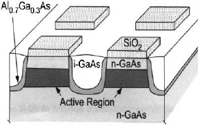
Figure 4. Schematic representation of the fabrication for a quantum-box array.
3. Preliminary experimental results
![]() Single-stage intersubband emitters
Single-stage intersubband emitters
Optimization of the QW material for efficient emission involves optimizing the QW structure shown in Fig. 2. We have already developed20 such a deep-well light-emitting structure, thus demonstrating the first room-temperature emission in the mid-IR (λ = 4.7μm) from a single-stage IS device – see Fig. 5. Electrons are injected, via resonant tunneling, from the ground level of the injector miniband into the upper level E3 of the active region. We have significant experience with resonant-tunneling structures, having demonstrated27 the first deep-well resonant tunneling diodes (RTD’s); that is, double-barrier diodes for which the quantum well, being compressively strained, has a conduction-band edge lower in energy than that for the injector and emitter regions. We have extended the deep-well approach to light-emitting intersubband devices20 in order to tightly confine the carriers to the active quantum well(s). In turn, carrier losses via thermionic emission and/or tunneling through the outer barrier are significantly suppressed. The FWHM spectral linewidths are 19 meV and 25 meV at 80 K and 300 K, respectively. These values are the same or better than the best results reported28 from conventional 5 μm-emitting QC structures grown by MBE. Thus the results confirm that we can grow IS light-emitting structures by MOCVD equal in crystalline quality to those grown by MBE.
More recently, we have grown strain-compensated 25-stage QC structures using the single-stage design of Fig. 2 and obtained excellent surface morphology and sharp x-ray diffraction spectra, shown in Fig. 6, indicative of excellent material quality and nearly perfect lattice match to the GaAs substrate.
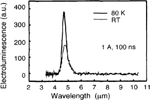
Figure 5. Intersubband electroluminescence spectra at 80 K and at RT.20

Figure 6. Experimental (top) and simulated (bottom) x-ray diffraction patterns for a 25-stage, strain-compensated, deep-well QC structure.

Figure 7. SEM of 26 nm-diameter SiO2 posts spaced 80 nm center-to-center.
![]() Quantum-box patterning
Quantum-box patterning
The eventual design involves a QB array of 30 nm diameter boxes spaced 60 nm center-to-center (Fig. 1), a nontrivial task. Therefore, the patterning has to be done in progressive steps. We used e-beam direct writing employing a novel hydrogen silsesquioxane resist; which was found best for generating high-quality 2D dot patterns: 33 nm-diameter dots spaced 80 nm center-to-center.26 This represents a 13% QB fill factor, well on the way to the 20% target value. Recently we achieved transfer of such patterns into SiO2, a dielectric thought suitable as a mask for in-situ etching and regrowth. The resulting 26 nm diameter, ~50 nm tall posts were obtained with 80 nm center-to-center spacing, see Fig. 7.
![]() Nanopost etching, in-situ gas etching and in-situ GaAs regrowth
Nanopost etching, in-situ gas etching and in-situ GaAs regrowth
Initial work involved an SiO2 mask on patterned GaAs substrates and dilute-HCl gas flow for in-situ etching.29 Controlled etching (~3 nm/sec) through narrow, SiO2-defined stripes reproducibly provided ~40 nm-deep trenches. However, when using structures with thin (2–3 nm), buried high-Al-content layers, the gas etching stopped at those layers due to oxidation29 most likely because residual oxygen in the etching ambient caused almost instantaneous AlOx formation on the surface, thus suppressing gas-phase etching. Therefore we proceeded to etch trenches in a dry-chlorine or BCl3-based plasma environment followed by a mild in-situ etching, to get rid of dry-etch-induced damage prior to regrowth. In particular, BCl3-based etching was found to provide the vertical walls necessary for the formation of the nanoposts required for (2–3)-QB stack devices. As shown in Fig. 8, 57 nm-diameter GaAs posts of 170 nm height were formed, spaced 200 nm center-to-center.
Scanning electron microscopy pictures of etched and regrown structures are shown in Fig. 9. The 33 nm-wide, 80 nm-tall ridges (Si3N4 + GaAs) were dryetched. see inset of Fig. 9(a). Then, in-situ gas etching and regrowth were performed, see Fig. 9(a). Similarly, 35 nm-diameter, 80 nm-tall posts (Si3N4 + GaAs) were also subjected to in-situ etch and regrowth, see Fig. 9(b). AFM measurements confirmed that 40 nm-tall Si3N4 posts are left after regrowth. For the actual device fabrication the Si3N4 posts would be removed via etching and the growth continued in order to obtain the structure shown in Fig. 1

Figure 8. SEM of dry-etched GaAs 57 nm-diameter posts, spaced 200 nm center-to-center.
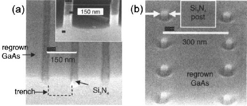
Figure 9. Structures subjected to in-situ etch and regrowth: (a) 33 nm-wide ridges, with dry-etched pattern before regrowth shown in the inset; (b) 35 nm-diameter Si3N4 posts left after regrowth.
![]() Fermi-level pinning elimination at in-situ etched and regrown interfaces
Fermi-level pinning elimination at in-situ etched and regrown interfaces
For unipolar intersubband devices such as QC lasers one need not be concerned about loss of carriers to defects at exposed surfaces, since the transition energies involved are much smaller than the energy between the midgap and the conduction-band edge at those exposed surfaces. Quantum cascade lasers with exposed 10 μm-wide ridges operate quite well. However, for nanostructures with in-plane dimensions of ≤ 50 nm the defect density needs to be drastically reduced at the device edges, since Fermi-level pinning would cause full depletion across the devices.30 Therefore, our QB formation will be done such that no charge-trapping states are formed at the QB edges, thus eliminating Fermi-level pinning.
We have carried out experiments on (110)-oriented GaAs substrates; that is on crystalline planes equivalent to the side edge(s) of the QBs to be formed. N-type (2×1017 cm-3) GaAs was grown and dry-plasma etched. The sample was then dipped in HCl to remove any residue from plasma, annealed in arsine in an MOCVD reactor, followed by an in-situ etch using HCl gas. A thin n-GaAs (1×1017 cm-3) film was then grown, as shown schematically in Fig. 10(a), and capacitance-voltage characterization carried out. The capacitance was recorded as a function of the applied voltage as the depletion width W moved across the etched and regrown interface. Fig. 10(b) shows the variation of the carrier concentration N vs. W. Presence of trap states at the interface would result in a decrease and subsequent increase in the apparent carrier concentration. Lack of any features in the N vs. W curve at the interface (that is, at W = 0.18 μm) indicates no trap states. This means that Fermi-level pinning has been eliminated for the proposed fabrication of intersubband QBs. It should be emphasized that samples without HCl dip and arsine annealing did exhibit trap states.

Figure 10. In-situ etching and regrowth on a (110) GaAs electron-cyclotron-resonance (ECR)-etched water: (a) schematic of the sample; (b) carrier concentration vs. depletion width W (arrow indicates the interface at W = 0.18 μm).
4. Conclusions
Significant suppression of phonon-assisted electron relaxation times in deep unipolar quantum boxes will allow the fabrication of intersubband lasers emitting cw at room temperature in the 3–13 μm wavelength range with high (> 40%) wallplug efficiency. Since the backfilling effect characteristic of cascaded QW lasers is a moot issue, IQB lasers are unlikely to suffer from the thermal runaway that currently mars the performance of cw QC lasers3,4,23 and thus should prove to be reliable devices. Preliminary results include the demonstration at the nanoscale of the in-situ (gas) etch and regrowth processes necessary for the IQB formation, and the development of a technique for preventing Fermi-level pinning during the QB fabrication.
Acknowledgments
This work was supported in part by SPAWAR under a DARPA contract.
References
- R. F. Kazarinov and R. A. Suris, “Possibility of the amplification of electromagnetic waves in a semiconductor with a superlattice,” Sov. Phys. Semicond. 5, 207 (1971).
- J. Faist, F. Capasso, D. L. Sivco, C. Sirtori, A. L. Hutchinson, and A. Y. Cho, “Quantum cascade laser,” Science 264, 553 (1994).
- A. Evans, J. S. Yu, S. Slivken, and M. Razeghi, “Continuous-wave operation at λ ~ 4.8 μm quantum-cascade lasers at room temperature,” Appl. Phys. Lett. 85, 2166 (2004).
- J. S. Yu, A. Evans, S. Slivken, S. R. Darvish, and M. Razeghi, “Short wavelength (λ ~ 4.3 μm) high-performance continuous-wave quantum-cascade lasers,” IEEE Photonics Technol. Lett. 17, 1154 (2005).
- J. Faist, A. Tredicucci, F. Capasso, et al., “High-power continuous-wave quantum cascade lasers,” IEEE J. Quantum Electronics 36, 336(1998).
- C.-F. Hsu, J.-S. O, P. Zory, and D. Botez, “Intersubband quantum-box semiconductor lasers,” IEEE J. Selected Topics Quantum Electronics 6, 491 (2000).
- U. Bockelmann and G. Bastard, “Phonon scattering and energy relaxation in two-, one-, and zero-dimensional electron gases,” Phys. Rev. B 42, 8947 (1990).
- H. Benisty, C.M. Sotomayor-Torres, and C. Weisbuch, “Intrinsic mechanism for the poor luminescence properties of quantum-box systems,” Phys. Rev. B 44, 10945(1991).
- R. Heitz, M. Grundmann, N. N. Ledentsov, et al., “Multiphonon-relaxation processes in self-organized InAs/GaAs quantum dots,” Appl. Phys. Lett. 68, 361 (1996).
- J. Urayama, T. B. Norris, J. Singh, and P. Bhattacharya, “Observation of phonon bottleneck in quantum dot electronic relaxation,” Phys. Rev. Lett. 86, 4930 (2001).
- L. Rebohle, F. F. Schrey, S. Hofer, G. Strasser, and K. Unterrainer, “Energy level engineering in InAs quantum dot nanostructures,” Appl. Phys. Lett. 81, 2079 (2002).
- S. Sauvage, P. Boucaud, R. P. Lobo, et al., “Long polaron lifetime in InAs-GaAs self-assembled quantum dots,” Phys. Rev. Lett. 88, 177402 (2002).
- Z.-K. John Wu, H. Choi, T. B. Norris, A. Stiff-Roberts, and P. Bhattacharya, “Ultrafast electronic dynamics in unipolar n-doped InAs/GaAs quantum dot structures,” paper QThC6 in: Proc. 2005 CLEO/QELS, Baltimore, MD (2005).
- Z.-K. John Wu, H. Choi, T. B. Norris, S. Chakrabarti, X. Su, and P. Bhattacharya, “Electron dynamics in n-doped In0.4Ga0.6As/GaAs quantum dot infrared detector structures,” paper QTuK3 in: Proc. 2006 CLEO/QELS, Long Beach, CA (2006).
- B. Kochman, A. D. Stiff-Roberts, S. Chakrabarti, et al., “Absorption, carrier lifetime, and gain in InAs-GaAs quantum-dot infrared photodetectors,” IEEE J. Quantum Electronics 39, 459 (2003).
- L. Jacak, J. Krasnyi, D. Jacak, and P. Machnikoski, “Magnetopolaron in a weakly elliptical InAs/GaAs quantum dot,” Phys. Rev. B 67, 035303 (2003).
- C.-F. Hsu, J.-S. O, P. S. Zory, and D. Botez, “Intersubband laser design using a quantum box array,” Proc. SPIE 3001, 271 (1997).
- I. A. Dmitriev and R. A. Suris, “Quantum cascade lasers based on quantum dot superlattice,” Phys. Stat. Sol. A 202, 987 (2005).
- I. C. Sandall, P. M. Smowton, C. L. Walker, H. Y. Liu, M. Hopkinson, and D. J. Mowbray, “Recombination mechanisms in 1.3 μm InAs quantum-dot lasers,” IEEE Photonics Technol. Lett. 18, 965 (2006).
- D. P. Xu, A. Mirabedini, M. D’Souza, et al., “Room-temperature, mid-infrared (λ = 4.7 μm) electroluminescence from single-stage, intersubband GaAs-based edge emitters,” Appl. Phys. Lett. 85, 4573 (2004).
- H. Yagi, K. Muranushi, N. Nunoya, T. Sano, S. Tamura, and S. Arai, “GaInAsP/InP strain-compensated quantum-wire lasers fabricated by CH4/H2 dry etching and organometallic vapor-phase-epitaxial regrowth,” Japan. J. Appl. Phys. 41, Part 2, L186(2002).
- C. Gmachl, F. Capasso, A. Tredicucci, D.L. Sivco, R. Kohler and A.Y. Cho, “Dependence of the device performance on the number of stages in quantum-cascade lasers,” IEEE J. Selected Topics Quantum Electronics 5, 808 (1999).
- M. Beck, D. Hofstetter, T. Aellen, et al., “Continuous wave operation of a mid-infrared semiconductor laser at room temperature,” Science 295, 301 (2002).
- N. S. Wingreen and C. A. Stafford, “Quantum-dot cascade laser: Proposal for an ultralow-threshold semiconductor laser,” IEEE. J. Quantum Electronics 33, 1170 (1997).
- C. H. Fischer, P. Bhattacharya, and P.-C. Yu, “Intersublevel electro-luminescence from In0.4Ga0.6As/GaAs quantum dots in quantum cascade heterostructure with GaAsN/GaAs superlattice,” Electronics Lett. 39, 1537 (2003).
- G. Tsvid, M. D’Souza, D. Botez, et al., “Towards intersubband quantum box lasers: E-beam lithography update,” J. Vac. Sci. Technol. B 22, 3214 (2004).
- A. Mirabedini, L. J. Mawst, D. Botez, and R. Marsland, “High peak-current-density strained-layer In0.3Ga0.7As/Al0.8Ga0.2 resonant tunneling diode grown by metal organic chemical vapor deposition,” Appl. Phys. Lett. 70, 2867 (1997).
- J. Faist, F. Capasso, C. Sirtori, et al., “High-power mid-infrared (λ = 5 μm) quantum cascade lasers operating above room temperature,” Appl. Phys. Lett. 68, 3680 (1996).
- D. Botez, F. Cerrina, T. Kuech, and P. Zory, “Intersubband quantum-box (IQB) lasers,” Final Rep. DARPA/SPAWAR Grant No 660-7558-203-2003524, 2004.
- M. A. Reed, J. N. Randall, R. J. Aggarwal, R. J. Matyi, T. M. Moore and A. E. Wetsel, “Observation of discrete electronic states in a zero-dimensional semiconductor nanostructure,” Phys. Rev. Lett. 60, 535 (1988).