
Appendix C
Computation of Resonances in the Power Distribution Network of a PCB
This appendix describes three methods for computing resonances in the Power Distribution Network (PDN) of PCBs, which consists of two parallel metallic plates separated by a dielectric substrate, also indicated as power bus. The structure of the PCB used for simulations is the same as that presented in Section 8.2. The first method is based on the cavity model, the second is based on a SPICE equivalent circuit, and the third is based on a 3D model for full-wave numerical electromagnetic codes. The computed results for three points on the PCB are compared for the case of a bare PCB and a PCB populated by decoupling capacitors. It is shown that the three methods provide the same results from a practical viewpoint.
C.1 Cavity Model
The cavity model developed for a microstrip patch antenna can be applied to a PDN having a rectangular power-bus structure, as demonstrated in reference [1]. In this very useful paper, rich in references, it is also demonstrated that the method can be extended to PCBs with arbitrary shape by applying the segmentation method, and a mathematical simplification is given. Herein, the basic mathematical expressions are provided.
The cavity method is based on the following assumptions:
(a) The close proximity between the two ground planes suggests that the E-field has only the z component and the H-field has only the xy components in the region bounded by the power and ground planes.
(b) The field in the aforementioned region is independent of the z coordinate for all frequencies of interest.
(c) The electric current in the plane must have no component normal to the edge at any point on the edge, implying a negligible tangential component of the H-field along the edge. In fact, if electric sources ![]() are present along the interface between a perfect conductor and a dielectric medium, the following equation holds:
are present along the interface between a perfect conductor and a dielectric medium, the following equation holds: ![]() . This means that the condition of considering the tangential magnetic field at the edge to be zero, Ht = 0, can be used.
. This means that the condition of considering the tangential magnetic field at the edge to be zero, Ht = 0, can be used.
The region between the two planes can therefore be treated as a cavity bounded by magnetic walls along the edges and by electric walls from above and below. This is also an important factor when building a model for numerical codes in order to speed up the computation. In fact, the condition Ht = 0 at the edge can be used instead of adding open field space.
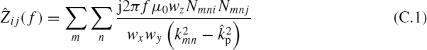
For a rectangular PCB like that shown in Figure C.1, the impedance matrix ![]() between two generic ports i and j placed at coordinates (xi, yi) and (xj, yj), respectively, and having an electrically small rectangular cross-section of size (Px0, Py0), can be obtained analytically by the expressions
between two generic ports i and j placed at coordinates (xi, yi) and (xj, yj), respectively, and having an electrically small rectangular cross-section of size (Px0, Py0), can be obtained analytically by the expressions
where


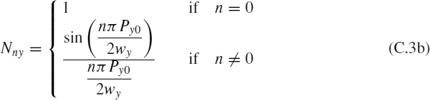


Nmnj has the same expression of Nmnj with j instead of i. In Equation (C.5), tan δ is the dielectric loss tangent, and r(f) is the skin depth at frequency f.
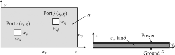
Figure C.1 Configuration of a rectangular PCB
These expressions provide the driving point impedance at port i, and the transfer impedance between ports i and j. Inspecting the various terms in (C.1)–(C.7), the following observations can be made:
- The term Nmni describes the wave physics associated with the cavity geometry.
- The terms in the double summation of Equation (C.1) are the propagating modes in the cavity and have modal resonant frequencies given by
- The term
 accounts for the dielectric and skin-effect conductor losses.
 - The double infinite summations must be truncated in practice. A trade-off between accuracy and time computation could be m = n = 20, as will be shown later.
- The computed impedance is valid for bare boards.

Impedance plots versus frequency are often used to evaluate the behavior of a power bus. In general, ![]() is defined as
is defined as

where ![]() is the voltage at a location on the power bus, labeled as port i, and
is the voltage at a location on the power bus, labeled as port i, and ![]() is the current at a location on the power bus, labeled as port j, and all other ports are open circuits, i.e.
is the current at a location on the power bus, labeled as port j, and all other ports are open circuits, i.e. ![]() for k ≠ j.
for k ≠ j.
Therefore, ![]() provides an indication of the voltage created by the injection of a noise current. On the other hand,
provides an indication of the voltage created by the injection of a noise current. On the other hand, ![]() indicates the noise transmission from a noise source to any-where on the board.
indicates the noise transmission from a noise source to any-where on the board. ![]() is very useful for circuit susceptibility and radiated emission studies. Although
is very useful for circuit susceptibility and radiated emission studies. Although ![]() is a complex quantity, often, for these types of study, it is just the magnitude that is considered.
is a complex quantity, often, for these types of study, it is just the magnitude that is considered.
For a PCB with three decoupling capacitors, as shown in Figure C.2 (the same as in Section 8.2), where the noise source is placed at port P1, the structure can be characterized by a five-port network: 1 and 2 are the observation ports, while 3, 4, and 5 are the ports associated with the decoupling capacitors. The Z matrix of the network can be written as

Figure C.2 PCB structure with two parallel planes modelled by MWS. Locations of ports (P) and decoupling capacitors (C) are shown

where ![]() is the vector containing the voltages at the observation ports, and
is the vector containing the voltages at the observation ports, and ![]()
![]() is the vector containing the voltages of the three decoupling capacitor ports. Note that Figure C.2 shows the model simulated by MWS, and the observation ports can be P1 and P2 or P1 and P3. For the ports concerning the decoupling capacitors, the currents are related to the voltages as
is the vector containing the voltages of the three decoupling capacitor ports. Note that Figure C.2 shows the model simulated by MWS, and the observation ports can be P1 and P2 or P1 and P3. For the ports concerning the decoupling capacitors, the currents are related to the voltages as
where ![]() is a diagonal matrix with the diagonal elements
is a diagonal matrix with the diagonal elements ![]() , i = 1, 2, 3. For this example (see Figure 8.12): R1 = 0.05 Ω, L1 = 5 nH, C1 = 1 μF; R2 = 0.05 Ω, L2 = 1 nH, C2 = 10 nF; R3 = 0.05 Ω, L3 = 8 nH, C3 = 10 nF. Inserting Equation (C.11) into Equation (C.10), and solving for
, i = 1, 2, 3. For this example (see Figure 8.12): R1 = 0.05 Ω, L1 = 5 nH, C1 = 1 μF; R2 = 0.05 Ω, L2 = 1 nH, C2 = 10 nF; R3 = 0.05 Ω, L3 = 8 nH, C3 = 10 nF. Inserting Equation (C.11) into Equation (C.10), and solving for ![]() , yields
, yields
where ![]() is the total impedance matrix of the two observation ports when the decoupling capacitors are accounted for.
is the total impedance matrix of the two observation ports when the decoupling capacitors are accounted for.
For the example considered, the voltages at the two observation points, computed by Equation (C.12), have the following matrix form:
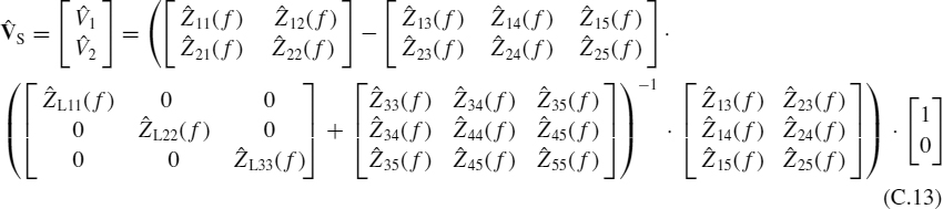
where the port impedances ![]() with i, j = 1, 2, …, 5 are calculated by the cavity model expression (C.1). With this formulation, two computations are required: port 1 with
with i, j = 1, 2, …, 5 are calculated by the cavity model expression (C.1). With this formulation, two computations are required: port 1 with ![]() and port 2 with
and port 2 with ![]() ; port 1 with
; port 1 with ![]() and port 3 with
and port 3 with ![]() . The application of this formulation to a PCB with more than three decoupling capacitors is straightforward, considering that the numeration for the capacitors starts from 3.
. The application of this formulation to a PCB with more than three decoupling capacitors is straightforward, considering that the numeration for the capacitors starts from 3.
C.2 Spice Model
When the quasi-static approximation can be used (i.e. when the dielectric separation d is much less than both the metal dimensions and the wavelength λ), each power and ground plane pair can be divided into unit cells of size ![]() and a lumped-element model can be assigned to each cell [2]. A cell consists of an equivalent circuit with R, L, C, and Gd components, as shown in Figure C.3.
and a lumped-element model can be assigned to each cell [2]. A cell consists of an equivalent circuit with R, L, C, and Gd components, as shown in Figure C.3.
Using the equation for a parallel plate [3], the equivalent circuit parameters of a unit cell are given by
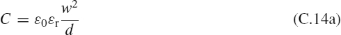
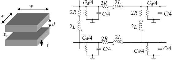
Figure C.3 Unit cell of power and ground planes and its equivalent circuit
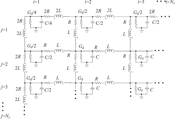
Figure C.4 Zoom of the upper left side of the board equivalent circuit
where C is computed by the parallel-plate capacitor expression, L is computed by using the property ε0εrε0w2 = LC, σc is the conductivity of the metal, Rdc = 2/(σct) is the resistance of the power and ground planes for a steady DC current, ![]() accounts for the skin effect on both conductors, and Gd represents the dielectric loss in the substrate (see Section 7.1 for these last two quantities).
accounts for the skin effect on both conductors, and Gd represents the dielectric loss in the substrate (see Section 7.1 for these last two quantities).
Using a distributed network of RLCGd elements, each rectangular power/ground plane pair can be divided into Nx × Ny unit cells. The upper left side of the equivalent circuit is shown in Figure C.4.
C.3 Numerical Model
The full-wave numerical simulation of the PCB structure shown in Figure C.2 was performed by the software tool MicroWave Studio (MWS) based on the finite integration technique [4]. The condition Ht = 0 was used at x and y direction edges and Et = 0 to simulate the planes, according to the explanation provided in Section C.1. This makes it possible to have a non-excessive number of mesh cells, and the simulation runs in a few minutes. The impedances ![]() ,
, ![]() , and
, and ![]() were calculated by placing a current source of 1 A at position 1 in Figure C.2 and computing the voltages at positions 1 (current source with I = 1 A), 2 (current source with I = 0) and 3 (current source with I = 0).
were calculated by placing a current source of 1 A at position 1 in Figure C.2 and computing the voltages at positions 1 (current source with I = 1 A), 2 (current source with I = 0) and 3 (current source with I = 0).
C.4 Results of the Simulations
The results of simulations performed with the three methods are shown in Figure C.5. Ports and decoupling capacitors have the locations indicated in Figure C.2. The following parameters were used for the cavity model: wx = 20.8 cm, wy = 15.6 cm, wz = 1.5 mm, εr = 4.25, ε0 = 8.854 × 10⁻¹² F/m, μ0 = 4π10−7 H/m, σc = 5.9 × 10⁷ S/m, tan δ = 0.02, mmax = nmax = 20, Px0 = Py0 = 1 mm. The parameters of the decoupling capacitors have the values reported in Section 8.2. The circuit parameters were computed by Equations (C.14), adopting Nx = 20 and Ny = 16, according to the notation of Figure C.2. As the computations were performed up to a frequency of 1 GHz, seeing as ![]() , the condition of an electrically short unit cell is verified.
, the condition of an electrically short unit cell is verified.
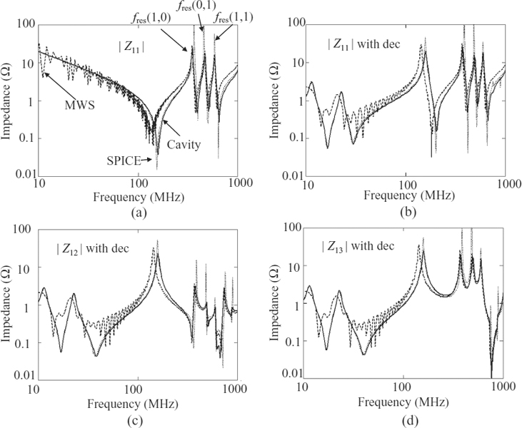
Figure C.5 Computed impedances: (a) at port 1 with bare board; (b) at port 1 with decoupling capacitors; (c) between ports 1 and 2 with decoupling capacitors; (d) between ports 1 and 3 with decoupling capacitors. Cavity model (solid line), SPICE (dotted line), MWS (dashed line)
Figure C.5 shows a good agreement among the curves obtained by the three methods. MWS presents fast oscillations in the low-frequency range because the simulation in the time domain is stopped at a time when the points of resonance are clearly visible in order to save computation time. Recall that MWS provides results in the frequency domain by FFT. When the cavity structure is highly resonant, as in this case, a long simulation time is necessary to have a low level of voltage oscillations at the required port and therefore stable impedance values at low frequencies. When the interest is mainly focused on the values of the resonance frequencies, the computation can be stopped at a convenient time, referring to the time and frequency results which are continuously displayed during the simulations. The three resonance frequencies with the bare boards correspond to the first modal resonance frequencies: fres(1, 0) = 350 MHz, fres(0, 1) = 467 MHz, fres(1, 1) = 583 MHz.
References
[1] Wang, C., Mao, J., Selli, G., Luan, S., Zhang, L., Fan, J., Pommerenke, D., DuBroff, R., and Drewniak, J., ‘An Efficient Approach for Power Delivery Network Design with Closed-form Expressions for Parasitic Interconnect Inductances’, IEEE Trans. on Advanced Packaging, 29 (2), May 2006, 320–334.
[2] Kim, J.-H. and Swaminathan, M., ‘Modeling of Multilayer Power Distribution Planes Using Transmission Matrix Method’, IEEE Trans. on Advanced Packaging, 25(2), May 2002 189–199.
[3] Pozar, M., ‘Microwave Engineering’, 2nd edition, John Wiley & Sons, Inc., New York, NY, 1998, Chapter 4.
[4] www.cst.com.
Signal Integrity and Radiated Emission of High-Speed Digital Systems Spartaco Caniggia and Francescaromana Maradei
© 2008 John Wiley & Sons, Ltd