
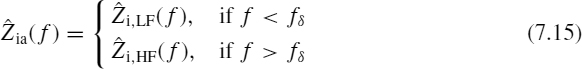
7
Lossy Transmission Lines
At high speed of actual digital devices, interconnects behave as lossy Transmission Lines (TLs) in which the effects of losses can seriously degrade Signal Integrity (SI) quality. Accurate and efficient simulation techniques are needed during design and verification to ensure that TLs do not affect correct operation. For this reason, the problem of considering losses in simulating TLs has come to prominence.
In this chapter, lossy line fundamental parameters are introduced and their effect on signal propagation is discussed. The reflection mechanism due to losses along interconnects such as PCB traces or cables is described by the segmentation approach based on the decomposition of the line into a series cascade of elementary circuit cells. Each cell includes an impedance, representing the effects of losses, and a lossless transmission line whose parameters are the nominal characteristic impedance and delay time associated with the corresponding lossless line segment. Losses due to skin, proximity, and dielectric effects are introduced, and the frequency range where they become significant is discussed. Closed-form expressions for calculating these losses are given, including the proximity effect which cannot be directly computed. A coefficient Kp is introduced into the skin-effect expression to take account of the proximity effect. This coefficient can be derived by using full-wave codes or analytically considering the procedure outlined in Appendix B for microstrip and stripline traces. An analytical circuit approach for predicting the step response of a lossy line is also provided. This approach consists in simulating the lossy behavior of the line in the frequency domain and then using the discrete Inverse Fourier Transform (IFT) to obtain results in the time domain. In this way, the effect of losses in slowing down the rise time of the traveling signal can be highlighted.
A good circuit model for the interconnect is critical for accurate and efficient analysis of the transient propagation of signals. For this reason, in the second part of this chapter, modeling procedures to perform simulation of a lossy line directly in the time domain are outlined. Two main modeling procedures are presented. The first procedure is based on the segmentation approach (i.e. the TL is decomposed into a series cascade of sections) and the Vector Fitting (VECTFIT) technique which allows an electrically short segment of the cable with frequency-dependent losses to be represented as a network of lumped-circuit elements independent of frequency. This network reproduces the effects of frequency-dependent losses in the time domain. By this model, lossy lines with non-linear loads can be simulated directly in the time domain. The drawback of this modeling procedure is that the length of the lossy lines must not be too large, to avoid memory and time problems during the simulations. The second procedure for modeling lossy TLs in the time domain is based on scattering parameters which can be measured or computed in the time domain as the response of a step source for the line length of interest. Then, by a simple circuit that performs numerical derivative, convolution integral, and delay functions, the signal integrity simulation of a point-to-point structure with non-linear loads can be obtained without limitation in length. The proposed models are validated by comparing simulated waveforms with those obtained by experimental measurements.
7.1 Lossy Line Fundamental Parameters
To have suitable models for simulating lossy lines is a fundamental requirement for designing high-speed digital systems. Many approaches can be found in the literature [1–20]. The aim of this chapter is to provide simple models that make it possible, with acceptable approximation, to reproduce the eye diagrams of signaling in PCBs and cables. To build up these models, it is essential to begin with the definition and characterization of the fundamental parameters of a lossy line in different ranges of frequency.
7.1.1 Reflection Mechanism in a Lossy Line
The equivalent circuit of a lossy transmission line may be represented by a cascade connection of electrically short lumped-circuit elements, as shown in Figure 7.1 [21, 22]. This circuit allows for frequency-constant losses and is described by the following parameters:
- Ri = the p.u.l. internal resistance accounting for losses due to the signal and return conductors;
- L0 = the p.u.l. external inductance;
- C0 = the p.u.l. shunt capacitance;
- Gd = the p.u.l. shunt conductance depending on the conductivity of the substrate material and representing losses in the dielectric surrounding the conductors.
The nominal characteristic impedance Z0 and the nominal velocity of propagation ν0 of a line are defined as the quantities associated with the line when losses are neglected. By this definition, if Z0 and ν0 are known, it is possible to calculate L0 and C0 as follows:

Figure 7.1 Lossy line equivalent circuit as a cascade connection of half-T cells
To understand how losses deteriorate the signal integrity of a transmitted signal across the line, the simple case of frequency-constant losses Ri = Rdc is considered, and the line is modeled as a series cascade of lossless TLs of characteristic impedance Z0 and propagation delay time tpdΔx, connected to the series resistance RdcΔx representing the DC losses associated with the signal and return conductors of length Δx. Each subsection of the line of length Δx should be very short, usually at least <λ/10, where λ is the minimum wavelength of interest.
Let us consider the instant at which the voltage source ES switches, and let us denote by VS the voltage generated after the source resistance RS. Owing to the partitioning effect between lumped resistances RS and RdcΔx and Z0, the amplitude of the voltage signal launched into the line is given by

Again, owing to the partitioning effect, the voltage launched onto the first TL has the value ηVS, where η is the transmission coefficient, as shown in Figure 7.2. When the step voltage ηVS reaches the other end of the TL, there is a reflected voltage ρηVS and a transmitted voltage ηVS(1 + ρ), where ρ is the refection coefficient, as shown in Figure 7.2. The voltage at the input of the second TL is η2VS(1 + ρ), and a new reflection of value ρηVS(1 + ρ) is generated. This mechanism occurs with each TL, and the total waveforms at source and load ends are the algebraic sum, with suitable delays, of a large amount of reflections of this type. All this can be better represented by the lattice diagram shown in Figure 7.2. Note that the signal at the input of each TL towards the load is increasingly smaller than the starting signal VS. This does not happen with lossless lines because the waveform that reaches the load is exactly the same as the waveform sent by the source.
In practical cases, the line p.u.l. internal resistance Ri has a more complicated expression than Ri = Rdc and depends on frequency owing to skin and proximity effects. In order to account for frequency-dependent losses, the total p.u.l. series impedance ![]() of any transmission line can be expressed as
of any transmission line can be expressed as
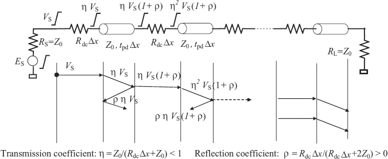
Figure 7.2 Reflection mechanism in a frequency-constant lossy line
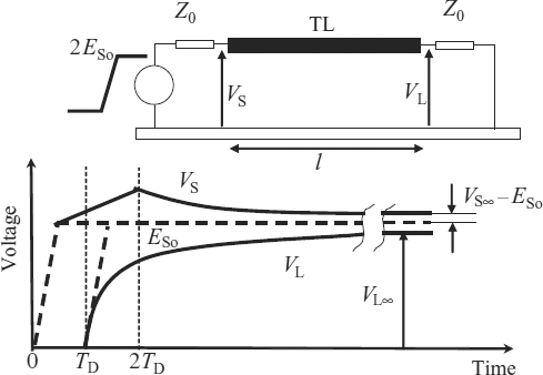
Figure 7.3 Typical source and load voltage waveforms for an interconnect matched at both ends: lossless TL (dashed line), frequency-dependent lossy TL (solid line)
where L0 is the p.u.l. external series inductance related to the magnetic flux external to the conductor, and ![]() is the line p.u.l. internal impedance.
is the line p.u.l. internal impedance.
The impedance ![]() is a frequency-dependent complex parameter consisting of a real resistive part increasing with the frequency and an imaginary part representing the internal inductance of the conductor which decreases with the frequency.
is a frequency-dependent complex parameter consisting of a real resistive part increasing with the frequency and an imaginary part representing the internal inductance of the conductor which decreases with the frequency.
In Section 7.2 it will be shown that, by analogy with the circuit in Figure 7.2, the series cascade of Zi(f)Δx and a lossless TL can be used to simulate a frequency-dependent lossy line in the time domain once an appropriate network for ![]() is derived. The network, which takes into account frequency-dependent losses, is extracted by the Vector Fitting (VF) technique and is composed of constant circuit elements R, L, and C in order to reproduce zeros and poles in the frequency domain of a small section of the interconnect.
is derived. The network, which takes into account frequency-dependent losses, is extracted by the Vector Fitting (VF) technique and is composed of constant circuit elements R, L, and C in order to reproduce zeros and poles in the frequency domain of a small section of the interconnect.
Figure 7.3 illustrates the differences between a lossless line and a typical frequency-dependent lossy line, in terms of voltage waveforms at the input VS and output VL of the line of length l matched at both ends, when the source is a step voltage with a linear rise time. For a lossless line, the waveforms are equal in shape and separated by the line delay time TD = tpdl. For a lossy line, VS is modified by reflections, rises to its maximum peak at time 2TD, and then decreases to its rest value VS∞ after a long period of time. Owing to the attenuation effect of the losses, VL rises more slowly to its rest value VL∞. Final values depend on the total DC resistance Rdcl of the line according to the equations


In Section 7.2 it will be shown that the set-up of Figure 7.3 is very useful for obtaining parameters in order to simulate the lossy line in the transient domain by a distributed model.
In general, different types of loss characterize the line and contribute to determining the line p.u.l. internal impedance ![]() :
:
- DC losses;
- skin effect;
- proximity effect;
- radiation effect (less important and not treated in this book).
Moreover, dielectric effects should be considered to obtain a more realistic modeling of the line p.u.l. admittance ![]() than that based on constant C0 and Gd as shown Figure 7.1. A detailed analysis of these losses will be outlined in the following sections.
than that based on constant C0 and Gd as shown Figure 7.1. A detailed analysis of these losses will be outlined in the following sections.
7.1.2 Skin Effect
The phenomenon of the skin effect is based on two facts: a current flowing in any real conductor produces an electric field given by Ohm’s law; the current distribution and/or magnetic field distribution in a conductor is frequency dependent. For DC current in a single isolated conductor, the current density is uniform across the conductor. When alternating current is used, the current density is not uniform across the conductor. The current tends to concentrate on the conductor surface. Current density continuously increases from the conductor center to its surface, but, for practical purposes, the current penetration depth, δ, is assumed to be a dividing line for current density. The current is assumed to flow in an imaginary cylinder of thickness equal to the penetration depth δ with a constant current density throughout the cylinder thickness. The distribution of current densities for both actual and simplified models is shown in Figure 7.4 [22].
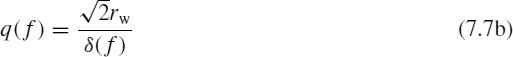
The penetration depth, expressed in meters and as function of the frequency f, is defined as
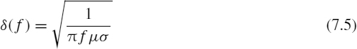
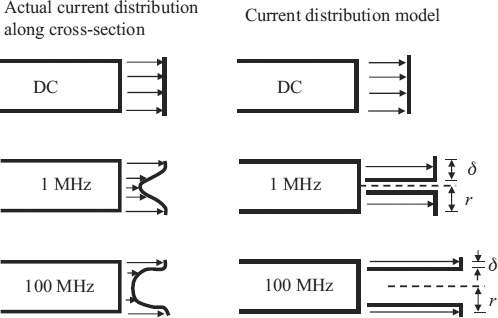
Figure 7.4 Skin effect: actual (left) and simplified (right) current distributions across a round conductor for several frequencies

Figure 7.5 Normalized skin depth δ/rw for a round copper wire of radius rw = 0.25 mm
where μ is the magnetic permeability of the conducting material (for air μ = μ0 = 4π10−7 H/m), and σ is the conductivity of the conducting material (for copper σCu = 5.8 × 10⁷ S/m).
The variation in the penetration depth with frequency is shown in Figure 7.5 for the case of a round wire of radius rw = 0.25 mm and copper material. The skin depth equals the radius at a frequency of 70 kHz and becomes 1/10 at a frequency of 8 MHz.
Because the skin effect reduces the equivalent conductor cross-sectional area, the frequency increase causes an increase in the p.u.l. effective resistance of the line. This in turn leads to an increasing attenuation with frequency. If the frequency response of a cable is plotted on log–log graph paper, log dB, or nepers versus log frequency, the curve slope will be 0.5 if the cable losses are primarily governed by classical skin effects. The slope of the attenuation curve, along with the attenuation at a particular frequency, can be used to estimate coaxial cable transient response as a function of length [22]. Losses in coaxial cable will be treated in Section 7.2.
7.1.2.1 Round Wires
The p.u.l. internal impedance ![]() for an isolated round wire can be calculated exactly by the following equation [23]:
for an isolated round wire can be calculated exactly by the following equation [23]:

where Ber(0, q(f)) and Bei(0, q(f)) are the real and imaginary parts of the complex Bessel function ![]() , and
, and


These equations can be conveniently computed by mathematical programs such as MathCad™. The equations are valid on the assumption of a ‘good conductor’ material for which ![]() at all frequencies of interest. This is the case for all practical conductors.
at all frequencies of interest. This is the case for all practical conductors.
At very low frequency or DC condition, the p.u.l. resistance Rdc and internal inductance Li,dc = Lint of the wire assume the values

where ![]() is the round wire area, and Rdc doubles if the return conductor is equal to the signal conductor.
is the round wire area, and Rdc doubles if the return conductor is equal to the signal conductor.
For low frequencies (LF), where the skin effect is not yet significant, q(f) is small and series expansions of the Bessel functions show that ![]() may be expanded as
may be expanded as

The p.u.l. resistance and internal inductance in the LF range are

The first term of RLF(f) is the DC resistance, and the second is a correction useful for radius equal to the skin depth δ. The term Li,LF(f) corresponds to the low-frequency internal inductance Li,dc of the wire.
For high frequencies (HF), where δ < rw, the argument q(f) is large. It may be shown that the high-frequency approximation of ![]() is [23]
is [23]

where f0 is a particular frequency, chosen well above the onset frequency of the skin depth but below the non-TEM mode region, p = 2πrw is the perimeter of the round wire, and R0 is the p.u.l. real part of the skin-effect impedance at f0.
It can be noted that, in the HF range, resistance and internal reactance are equal.
The term Rsurf(ω)/(2πrw) in Equation (7.11) denotes the p.u.l. resistance of a round wire when the total current is assumed to be concentrated in an annular surface of thickness δ [24].

The resistive and inductive parts at high frequencies are given by [25]
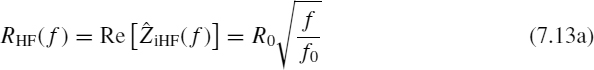
Note from Equation (7.5) that the skin depth decreases with increasing frequency as the inverse square root of the frequency. Thus, the high-frequency resistance RHF(f) increases at a rate of 10 dB/decade. The resistance remains at the DC value up to the frequency where these two asymptotes meet, or rw = 2δ(fδ). The skin-effect frequency fδ can be found by solving the equation Rdc = RHF(fδ) and is given by
Equation (7.13b) shows that the high-frequency internal inductance Li,HF decreases at a rate of 10 dB/decade after frequency fδ. Below this frequency the internal inductance has a constant value (Equation (7.10b)).
For the purposes of computation by mathematical programs, ![]() can be defined by three different approximate formulae [25]:
can be defined by three different approximate formulae [25]:
Comparison of the exact method (Equation (7.6)) for round wire and approximate methods (Equations (7.15)–(7.17)) is shown in Figure 7.6. It can be seen that ![]() and
and ![]() practically coincide with the exact impedance
practically coincide with the exact impedance ![]() , while
, while ![]() is significantly different in the transition region from DC to the high-frequency region where the skin effect dominates. The imaginary part tracks upwards as if it were an inductor of value Li,dc under the skin-effect onset frequency fδ. Real and imaginary parts match above fδ; both track upwards at +10 dB/decade. From now on, the approximation
is significantly different in the transition region from DC to the high-frequency region where the skin effect dominates. The imaginary part tracks upwards as if it were an inductor of value Li,dc under the skin-effect onset frequency fδ. Real and imaginary parts match above fδ; both track upwards at +10 dB/decade. From now on, the approximation ![]() will be used for computations. The above expressions can also be used, with good approximation, for other conductors of different shape but having area a and perimeter p.
will be used for computations. The above expressions can also be used, with good approximation, for other conductors of different shape but having area a and perimeter p.
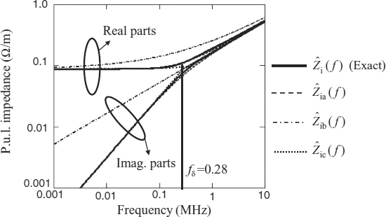
Figure 7.6 Skin-effect impedances computed by exact and approximate methods for a round copper wire of 1 m length and 0.25 mm radius
7.1.2.2 Rectangular Conductors
For a rectangular conductor such as a trace in a PCB, expression (7.17) of ![]() can be used, adopting in the computation the following perimeter and area:
can be used, adopting in the computation the following perimeter and area:
where w and t are the width and thickness of the rectangular conductor respectively.
This procedure can be used, as, similarly to the case of round wires, the current becomes concentrated in a thickness equal to one skin depth at the surface as the frequency increases. Actually, the current also peaks at the corners, but this fact may be practically neglected to simplify the computation. As for wires, the skin effect becomes significant when the thickness of the smaller dimensions equals two skin depths.
7.1.3 Proximity Effect
The proximity effect is the current density redistribution in a conductor owing to the mutual repulsion (or attraction) generated by currents flowing in nearby conductors [25]. The current density at those points on the conductor close to neighboring conductors is different than that occurring in isolated conductors. This current density redistribution reduces the effective cross-sectional area of the conductor, thereby increasing the p.u.l. resistance. This effect is a function of the conductor diameters, the separation of the conductors from each other, and frequency. Analytical evaluation of the proximity effect is quite complicated, and, except for certain limited cases, no general rule-of-thumb expressions have been proposed. The proximity effect is not present in coaxial cables because of their circular symmetry. The proximity effect is a significant contributor to signal losses, particularly in cases of twisted-pair cables or parallel wire lines such as in ribbon and twinax cables.
Figure 7.7 Proximity-effect example: computed tangential H-field to show the surface current (peak) at 5 GHz in an unshielded twisted-pair cable
As an example, the surface current at the frequency f = 5 GHz in a two-twisted-pair line computed by a full-wave numerical code is shown in Figure 7.7. The currents in each wire are equal but of opposite sign, and therefore surface currents are higher in the internal part of the cable.
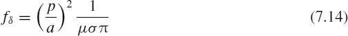
To take into account analytically the proximity effect, a factor Kp is introduced into the equations used for skin-effect computations. In practice, expression (7.11a) of the high-frequency internal impedance is still valid, with the only exception that in this case the real part of skin-effect impedance R0 is given by [25]
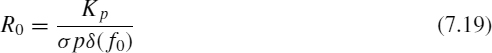
where the proximity-effect factor Kp is present. Equation (7.19) is valid for operating frequency f > fδ, where fδ is the starting frequency for skin and proximity effects, which can be derived by analogy with Section 7.1.2.1, and is given by

It is important to consider the following points:
- Kp = 1 for any conductor well separated from its return path.
- Kp increases as the conductor and its return path are brought closer.
- Kp may be computed by numerical codes, as analytical expressions are not available.
As will be shown by some examples, factor Kp can be obtained by TDR measurements (see Section 11.1), by numerical simulations (see Section 7.2), or by an indirect analytical approach as described in Appendix B for microstrip and stripline traces. Anyway, values of Kp for typical cables and traces used in PCBs are given by Johnson and Graham [25].
7.1.4 Lossy Dielectric Effect
If a time-harmonic voltage ![]() is applied to a material of surface area a and thickness h, the corresponding current
is applied to a material of surface area a and thickness h, the corresponding current ![]() is given by [25]
is given by [25]
where ω = 2πf is the angular frequency in rad/s, σ is the conductivity of the material in S/m, and ε is the permittivity of the material in F/m.
The current is therefore the sum of a term in-phase with the voltage source called the conduction current (it behaves like a resistor) and a term in-quadrature with the voltage source called the displacement current (it behaves like a capacitor).
For a good conductor, ![]() , which means that the current flows mostly in-phase with the voltage. Both σ and ε stay fairly constant over a wide range of frequency. For any conductor there is a critical frequency fc = σ/(2πε) above which the displacement current dominates and the material mostly acts like a capacitor. Any material that operates at a frequency well above fc is classified as a good insulator. For this material, the ratio σ/ωε remains nearly constant. Equation (7.21) can also be written as
, which means that the current flows mostly in-phase with the voltage. Both σ and ε stay fairly constant over a wide range of frequency. For any conductor there is a critical frequency fc = σ/(2πε) above which the displacement current dominates and the material mostly acts like a capacitor. Any material that operates at a frequency well above fc is classified as a good insulator. For this material, the ratio σ/ωε remains nearly constant. Equation (7.21) can also be written as
where ![]() is the complex permittivity of a material, the real part of which ε′ = ε is related to the displacement current, while the imaginary part ε″ = σ/ω is related to the conduction current. For a good insulator, the imaginary part ε″ is much smaller than the real part ε′. In practice, for a good insulator, two parameters are specified:
is the complex permittivity of a material, the real part of which ε′ = ε is related to the displacement current, while the imaginary part ε″ = σ/ω is related to the conduction current. For a good insulator, the imaginary part ε″ is much smaller than the real part ε′. In practice, for a good insulator, two parameters are specified:
- the dielectric permittivity of the material ε′ = ε;
- the dielectric loss tangent tan θ, defined by
Many textbooks tabulate the loss tangent for different materials and different frequencies, but the main properties of the dielectric loss tangent are as follows:
- It remains stable for a broad range of frequency.
- It has a positive value.
Note that in this chapter the loss tangent is referred to as tan θ to avoid confusion with the skin depth notation, but in the literature it is widely denoted by tan δ. For a typical FR4 substrate of a PCB, tan θ = 0.02. For tan θ < 0.05, it is possible to use the approximation tan θ ≈ θ.
The permittivities of free space and air are considered practically the same and assume the value ε0 = 8.854 × 10⁻¹² F/m. Therefore, the complex relative permittivity ![]() of the substrate of a PCB or of the insulation material in a cable is defined as
of the substrate of a PCB or of the insulation material in a cable is defined as

In the case of non-dispersive dielectric materials, the real part of the complex relative permittivity is equal to the relative dielectric permittivity εr. When the dispersion needs to be considered, as in the case of PCBs with a very high working frequency, more sophisticated models such as Debye may be used to describe the relative permittivity of the medium, and the real part of the complex relative permittivity in Equation (7.24) no longer coincides with εr [26, 27].
Looking at the line of Figure 7.1 and applying these last concepts, the shunt current for an electrically short section of length Δx can be represented by the equation
where ![]() is the p.u.l. complex dielectric admittance of the transmission line, which includes the effects of the capacitance C0 and of the conductance Gd. To obtain an analytical expression for
is the p.u.l. complex dielectric admittance of the transmission line, which includes the effects of the capacitance C0 and of the conductance Gd. To obtain an analytical expression for ![]() , the following considerations should be taken into account. The phase of the complex permittivity is −θ constant over a wide frequency range; then the log–log slope of the magnitude of the permittivity over that range must be very close to −(2/π)θ, as stated by Bode in the general theory of phase/magnitude relations. Therefore,
, the following considerations should be taken into account. The phase of the complex permittivity is −θ constant over a wide frequency range; then the log–log slope of the magnitude of the permittivity over that range must be very close to −(2/π)θ, as stated by Bode in the general theory of phase/magnitude relations. Therefore, ![]() can be represented as [25]
can be represented as [25]
where k is an arbitrary real constant. Starting from this assumption, it can be shown that the dielectric complex admittance ![]() is given by [25]
is given by [25]

where ω0 = 2πf0 is the angular frequency chosen in the frequency range where the lossy dielectric effect is significant, and θ0 is the dielectric loss tangent at frequency f0.
Another approach is that reported by Paul [24] with reference to the case of a structure in a homogeneous medium. According to this approach, the capacitance is proportional to the cross-sectional dimensions and the permittivity of the dielectric, and therefore, using εr and tan θ definitions, the following equation holds:

As previously outlined, numerous handbooks tabulate the loss tangent for different materials and different frequencies. As, for FR-4, which is usually used to construct PCBs, the loss tangent is fairly constant at high frequencies and is approximately 0.02, the p.u.l. conductance Gd(ω) can be written as
This result only applies to lines in a homogeneous medium, but the following consideration may be extended to lines in an inhomogeneous medium. With the loss tangent tan θ practically constant, observe that the p.u.l. conductance increases directly with frequency, 20 dB/decade, instead of the 10 dB/decade of the skin-effect resistance.
It should be pointed out that, in model (7.27), both conductance and capacitance are frequency dependent. On the other hand, in Equation (7.28) the capacitance is constant and equal to the nominal line parameter C0 of a lossless line, while the conductance is frequency dependent according to Equation (7.29). The two models produce the same conductance, as will be shown in Example 7.1.
7.1.5 Data Transmission with Lossy Lines
The main goal with lossy lines in high-speed digital links is to have methods for predicting, in the time domain, the deteriorations in the transmitted data caused by the different types of loss, which depend on frequency. To do this, the first step is to investigate the transmission-line properties in the frequency domain, which can be done by considering the transfer function of a line of length l matched at both ends [25]:
where ![]() is the transmission-line propagation coefficient, given by
is the transmission-line propagation coefficient, given by
In Equation (7.31), ![]() and
and ![]() are the p.u.l. impedance and admittance of the line. Note that one of the significant effects of losses is that the amplitude of each of the sinusoidal waves that comprise the time-domain signal is attenuated as they travel down the line. This is given by the real part of
are the p.u.l. impedance and admittance of the line. Note that one of the significant effects of losses is that the amplitude of each of the sinusoidal waves that comprise the time-domain signal is attenuated as they travel down the line. This is given by the real part of ![]() . The attenuation in dB is usually defined in two ways:
. The attenuation in dB is usually defined in two ways:

Therefore, 1 neper = 8.6858896 dB. The velocity of propagation can be computed as
This means that, as digital pulses are composed of a large number of sinusoidal components that travel down the line at different speeds and reach the load with different amplitudes, the starting pulse signal will be reconstructed on the load with distortion. This is called dispersion. It will be shown that losses attenuate the higher-frequency components more than the lower-frequency components. Hence, the bandwidth of the pulse is reduced and the pulse rise/fall times are increased.
The other important parameter of an interconnect is the complex characteristic impedance, defined as
7.1.5.1 AC Analysis of Loss Influence on TL Performance
In this section an investigation is made of the influence of different types of loss in the whole frequency range starting from DC to very high frequency [25].
For traces in PCBs and cables, three regions can be distinguished where, in turn, the DC effect, the skin plus proximity effect, and the dielectric effect become significant. Adopting this subdivision of the frequency spectrum, the p.u.l. impedance and admittance can be summarized as


where L0 and C0 are the p.u.l. line external inductance and capacitance, Rdc is the p.u.l. DC line resistance given by Equation (7.8a), ![]() is the p.u.l. frequency-dependent internal impedance of the line according to expression (7.17), and
is the p.u.l. frequency-dependent internal impedance of the line according to expression (7.17), and ![]() is the p.u.l. line admittance accounting for frequency-dependent dielectric losses given by Equation (7.27).
is the p.u.l. line admittance accounting for frequency-dependent dielectric losses given by Equation (7.27).
(i) DC Region
In the first region, also called the LC region, the propagation coefficient and the characteristic impedance of the TL are given by

For practical purposes, this is the region characterized by fLC < f < fδ, with fLC = Rdc/(2πL0), and fδ is given by Equation (7.20). In this case, the characteristic impedance (Equation (7.37b)) is approximately equal to the nominal characteristic impedance of a lossless line, i.e. ![]() .
.
Below the frequency fLC, another region, called the RC region, should be considered, where only the line parameters Rdc and C0 are significant. As the study of this type of region is beyond the scope of this book, the reader can find details about the general behavior within the RC region in the work by Johnson and Graham [25].
(ii) Skin- and Proximity-Effect Region
This second region is defined in the frequency range fδ < f < fθ, where fδ is the onset frequency of the skin and proximity effect given by Equation (7.20), and fθ is the onset frequency of the dielectric effect, the definition of which is given in the following frequency region. The propagation coefficient and the characteristic impedance of the TL are given by

It can be shown that the attenuation, in neper/m, is [25]

where R0 is given by Equation (7.19). To obtain Equation (7.39), it was assumed that ![]()
![]() , which is reasonable in the frequency range of interest.
, which is reasonable in the frequency range of interest.
(iii) Dielectric-Effect Region
In this region the propagation coefficient and the characteristic impedance of the TL are given by

It can be shown that the attenuation, in neper/m, is [25]

where θ0 is the angle corresponding to the dielectric loss tangent tan θ at the frequency f0. This region begins with the frequency fθ. The definition of fθ comes equating the attenuation of the skin and dielectric regions and neglecting the slowing varying term (ω/ω0)−θ0/π, so that

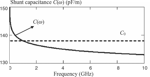
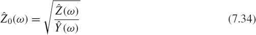
Figure 7.8 Shunt capacitance as a function of frequency
Example 7.1: Trace with 50 Ω Characteristic Impedance
For discussion purposes, consider a copper trace in a PCB with the following characteristics [25]: size 0.150 mm × 0.0174 mm; length l = 1 m; L0 = 346 nH; C0 = 138 pF; tan θ0 = 0.025 at f0 = 1 GHz; Kp = 1. These parameters give Z0 = 50 Ω, Rdc = 6.6 Ω, fLC = 3 MHz, fδ = 71.9 MHz, and fθ = 205.6 MHz. The response of the trace up to 10 GHz is calculated.
The frequency-dependent capacitance C(ω) obtained by Equation (7.27) is compared with the nominal capacitance C0 in Figure 7.8. Note that the capacitance decreases slightly with increasing frequency in the frequency range where the dielectric effect becomes significant, in other words, above 205.6 MHz. The p.u.l. shunt resistance Rd(ω) = 1/Gd(ω) obtained by the two models (7.27) and (7.29) is plotted in Figure 7.9. The two approaches provide the same results.
The real part of the complex characteristic impedance ![]() is plotted in Figure 7.10 for the three types of region discussed above. The imaginary part (not plotted) goes to zero at 100 MHz. Note that the characteristic impedance approaches its nominal value
is plotted in Figure 7.10 for the three types of region discussed above. The imaginary part (not plotted) goes to zero at 100 MHz. Note that the characteristic impedance approaches its nominal value ![]() at about 10 MHz.
at about 10 MHz.
The propagation coefficient ![]() , with its real (attenuation) and imaginary (phase) parts, versus frequency is shown in Figure 7.11 for the PCB trace considered. The case denoted as
, with its real (attenuation) and imaginary (phase) parts, versus frequency is shown in Figure 7.11 for the PCB trace considered. The case denoted as ![]() considers all kinds of loss. The scale is logarithmic for both frequency and propagation coefficient. Below fLC, both attenuation and phase rise together in proportion to the square root of frequency. Above fL, phase grows linearly with increasing frequency for each type of loss, while attenuation is flat when DC lossy is considered only.
considers all kinds of loss. The scale is logarithmic for both frequency and propagation coefficient. Below fLC, both attenuation and phase rise together in proportion to the square root of frequency. Above fL, phase grows linearly with increasing frequency for each type of loss, while attenuation is flat when DC lossy is considered only.

Figure 7.9 Shunt resistance Rd as a function of frequency, obtained by the two different models (7.27) and (7.29)
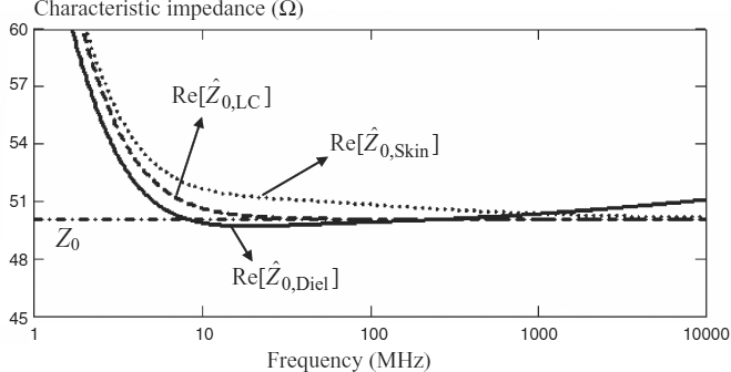
Figure 7.10 Real part of complex characteristic impedance
When skin-effect losses are considered above fδ, the attenuation curve has a slope proportional to the square root of frequency (dotted line). When dielectric-effect losses are considered above fθ, the attenuation curve tends to a slope proportional to the frequency (solid line). The plot also shows the case of ![]() calculated without considering the internal impedance (longer dashed line), in other words, considering the dielectric losses only. The slope of this curve is proportional to the frequency. Above fθ, dielectric losses dominate. A smooth arc represents the slope change from one region to another.
calculated without considering the internal impedance (longer dashed line), in other words, considering the dielectric losses only. The slope of this curve is proportional to the frequency. Above fθ, dielectric losses dominate. A smooth arc represents the slope change from one region to another.

Figure 7.11 Propagation coefficients plotted as a function of frequency
7.1.5.2 Step Response of a Lossy Line
As there are no analytical time-domain formulations to compute the step response of a line including all kinds of frequency-dependent loss, the traditional way to analyze lossy inter-connect is to perform the calculation in the frequency domain and then move the solution to the time domain by the Inverse Fast Fourier Transform (IFFT). To do this, three steps are required:
- Fourier transform representation in the frequency domain of a pulse with finite rise and fall times;
- frequency-domain solution of transmission-line equations of a lossy line loaded at both ends;
- inverse Fourier transform of the frequency-domain results to obtain time-domain solutions.
The procedure is outlined considering the same PCB trace as used in Example 7.1. The goal is to compute the step response at the end of the matched trace of length l = 0.5 m considering the different types of loss. The step is characterized by a pulse width tpw = b = 40 ns and a rise time tr = 0.05 ns. The computation of the pulse function Fourier transform and its implementation in MathCad™ are reported in Table 7.1 [25].
The following values were used in the simulation: Δt = 0.01 ns, m = 13, b = 40 ns, τ = 1 ns, tr = 0.05 ns. With these values, the number of points in the time domain is N = 8192, and therefore the pulse has a duration NΔt = 81.92 ns. The frequency step is Δf = 12.207 MHz. By using MathCad™, the IFFT of the pulse DFT must be normalized to 1/(NΔt). To obtain the pulse source signal, including the starting delay and linear rise time, the computation in the frequency domain is performed by MathCad™ notations:
Table 7.1 Implementation of Fourier transform for computation of a step response of a lossy line in MathCad™

Figure 7.12 Computed impulse: (a) full view; (b) detail of the rise time
XLrk := PulNk · Dlyk · Lrk
where XLr is a vector of index k and ‘:=’ means ‘=’. The pulse source in the time domain can be obtained by the IFFT with the suitable normalization required by MathCad™ as
![]()
where xLr is a vector of index n. The computed source is shown in Figure 7.12. The step response at the load end can be computed as the IFFT of the transfer function ![]() multiplied by the impressed voltage
multiplied by the impressed voltage ![]() , under the assumption that RS = 0. The propagation term
, under the assumption that RS = 0. The propagation term ![]() with the losses of interest is assigned at
with the losses of interest is assigned at ![]() . For example, in MathCad™ notations
. For example, in MathCad™ notations
![]()
where xDiel is a vector of index n that includes all kinds of loss.
The voltage VL(t) computed at time tn has the values provided by the component of index n of the vector xtype, where ‘type’ could be LC, Skin, Diel or Diel only, according to the definition of the propagation constant ![]() . The results are shown in Figure 7.13. Note that, for the case of DC losses only (i.e. the LC region), the load voltage is practically a translation of the source step with the rise time tr = 50 ps. Taking into account the skin effect, the load voltage has a delay very close to the delay of a lossless or LC line and a sharper initial rise time owing to the larger magnitude of its high-frequency content, but a slowly evolving tail owing to its frequency response near DC. By accounting for dielectric losses, there is an anticipation of the voltage step on the load owing to the fact that at very high frequencies (i.e. above fθ) the propagation velocity of the transmission line slightly exceeds the nominal value v0 and the rise time increases significantly (from 10 to 90 %). This is not visible in Figure 7.11 owing to the scale chosen.
. The results are shown in Figure 7.13. Note that, for the case of DC losses only (i.e. the LC region), the load voltage is practically a translation of the source step with the rise time tr = 50 ps. Taking into account the skin effect, the load voltage has a delay very close to the delay of a lossless or LC line and a sharper initial rise time owing to the larger magnitude of its high-frequency content, but a slowly evolving tail owing to its frequency response near DC. By accounting for dielectric losses, there is an anticipation of the voltage step on the load owing to the fact that at very high frequencies (i.e. above fθ) the propagation velocity of the transmission line slightly exceeds the nominal value v0 and the rise time increases significantly (from 10 to 90 %). This is not visible in Figure 7.11 owing to the scale chosen.
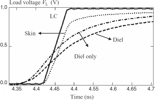
Figure 7.13 Computed time response VL(t) at the load end of the line for several types of loss
The considerations outlined are valid in the particular case of RS = 0 and RL = Z0. For general cases, transmission-line equations with terminal conditions need to be solved. After simple mathematical steps [25], the load voltage of a line excited by a source with a generic impedance ![]() and terminated on a generic load impedance
and terminated on a generic load impedance ![]() in the frequency domain is given by
in the frequency domain is given by

The input impedance of the line is

and the voltage at the line input in the frequency domain is
The time-domain voltages VS(t) at the line input and VL(t) on the load can be obtained by the IFFT of the corresponding frequency-domain expressions (7.45) and (7.43).

Figure 7.14 Computed voltage waveforms with (a) the line matched at both ends and (b) the line open at one end (i.e. TDR response)
Using the same PCB trace with the parameters Δt = 0.005 ns and m = 14 for better accuracy, ESo = 1 V, and the line matched at both ends to reproduce the typical waveforms of Figure 7.3, the results shown in Figure 7.14a are obtained. The source and load waveforms tend respectively to the limit values (see Equation (7.4) and Figure 7.3):

The computed waveform of the voltage VS(t) when the trace is open at one end is shown in Figure 7.14b. This waveform is useful, as it can be compared with TDR measurements in order to determine the coefficient Kp for modeling by closed-form expressions the losses of a line including the proximity effect. A detailed description of this calculation is presented in Section 11.1.3 for the case of microstrip and stripline trace structures. Another method is described in Appendix B.
7.2 Modeling Lossy Lines in the Time Domain by the Segmentation Approach and Vector Fitting Technique
To have appropriate lossy line models to simulate practical interconnects is strategic in order to verify if the data transmission specifications are met. It is also very important to have models suitable for performing a simulation directly in the transient domain without using the Fast Fourier Transform.
Different approaches can be found in the literature for lossy line modeling in the transient domain [1–20]. However, in this book, two methods suitable for implementation in a Spike-like simulator are outlined:
- the Vector Fitting (VF) technique applied in the frequency domain to a short section of cable for equivalent circuit extraction [28, 29];
- the Scattering (S) parameters technique applied in the time domain to the full length of the cable [30].
The VF technique will be outlined in this section for two kinds of cable structure: coaxial cables where the skin-effect losses can be represented by closed-form analytical equations, and twisted-pair cables where the lossy line parameters must be obtained by a full-wave numerical tool. The same approach can be applied to other types of interconnect such as ribbon, twinax cables, and PCBs. The scattering parameters technique will be described in Section 7.3.
7.2.1 Circuit Extraction of Coaxial Cables
The configuration considered here is a coaxial cable over a ground plane, as shown in Figure 7.15. The radii of the inner wire and the internal and external shields are rc, rsi, and rse. The inner wire conductor and the shield have conductivities and permeabilities σc, μ0, σs, and μs respectively. The relative permittivity of the dielectric is εrd.
The coaxial cable over a ground plane can be considered as a Multiconductor Transmission Line (MTL) of two independent conductors, and two different notations associated with the mesh and phase representations for voltages and currents can be adopted.
In particular, the most largely used mesh representation is based on considering two loops: the inner loop defined by the inner conductor and the internal shield, and the outer loop defined by the external shield and the ground plane. The mesh representation adopts the following notation:
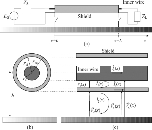
Figure 7.15 Coaxial cable over a ground plane: (a) longitudinal view; (b) transversal view; (c) phase and mesh currents and voltages
| wire-to-shield voltage; | |
| shield-to-ground voltage; | |
| current in the inner loop flowing in the internal wire and returning through the shield internal surface; | |
| current in the outer loop flowing in the shield external surface and returning through the ground plane; | |
| per-unit-length mesh impedance matrix; | |
| per-unit-length mesh admittance matrix. |
The second notation refers to the phase representation of voltage and currents and is defined by the following symbols:
| voltage between the internal wire and the ground plane; | |
| voltage between the external surface of the shield and the ground plane; | |
| current on the inner wire and returning through the ground plane; | |
| current on the shield and returning through the ground plane; | |
| per-unit-length phase impedance matrix; | |
| per-unit-length phase admittance matrix. |
Note that in mesh representation the voltage of the inner wire refers to the shield, while the voltage of the shield refers to the ground plane. On the other hand, in the phase representation the ground plane represents the unique reference for the voltages.
The link between voltages and currents used in the two representations can be easily derived by Figure 7.15 and is given by
which can also be written in matrix form as
where
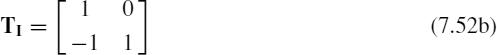
In the following, the mesh representation will be used. Phase representation could be required when loads between the inner wire and ground are present. However, loads of this kind can be easily taken into account by using a suitable termination network which can be derived by Equations (7.48) and (7.49) as described elsewhere [31].
The frequency-domain MTL equations describing the cable over the ground plane adopting the mesh representation are given by


7.2.1.1 Coaxial Cable Simulation Model
In Equation (7.53), the p.u.l. symmetric mesh representation impedance is given by
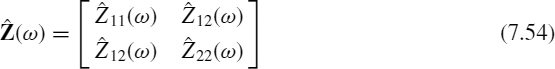
where ![]() and
and ![]() are the self-impedances of the two meshes, and
are the self-impedances of the two meshes, and ![]() is the mutual impedance between the meshes related to the cable transfer impedance.
is the mutual impedance between the meshes related to the cable transfer impedance.
The p.u.l. symmetric admittance matrix in Equation (7.53) is

where ![]() and
and ![]() are the self-admittances of the two meshes, and
are the self-admittances of the two meshes, and ![]() is the mutual impedance between the meshes related to the cable transfer admittance. The coefficients of the impedance and admittance matrices are explicitly given below [32, 33].
is the mutual impedance between the meshes related to the cable transfer admittance. The coefficients of the impedance and admittance matrices are explicitly given below [32, 33].
Coefficient ![]() – This coefficient is the p.u.l. impedance of the inner loop formed by the inner wire and the shield. It is the sum of three terms:
– This coefficient is the p.u.l. impedance of the inner loop formed by the inner wire and the shield. It is the sum of three terms:
where ![]() is the p.u.l. impedance of the inner wire,
is the p.u.l. impedance of the inner wire, ![]() is the p.u.l. external impedance between inner wire and shield, and
is the p.u.l. external impedance between inner wire and shield, and ![]() is the p.u.l. internal impedance of the shield.
is the p.u.l. internal impedance of the shield.
These impedances are given by


where ![]() is the p.u.l. DC resistance of the inner wire,
is the p.u.l. DC resistance of the inner wire, ![]() is the skin depth of the internal wire, Rsi,dc = 1/(2πσsrsid) is the p.u.l. DC resistance of the internal shield,
is the skin depth of the internal wire, Rsi,dc = 1/(2πσsrsid) is the p.u.l. DC resistance of the internal shield, ![]() is the skin depth of the shield, and d = rse − rsi is the shield thickness.
is the skin depth of the shield, and d = rse − rsi is the shield thickness.
Coefficient ![]() – This coefficient is the impedance of the outer loop formed by the shield and the ground plane. It is the sum of two terms:
– This coefficient is the impedance of the outer loop formed by the shield and the ground plane. It is the sum of two terms:
where ![]() is the p.u.l. internal impedance of the external shield and
is the p.u.l. internal impedance of the external shield and ![]() is the p.u.l. external impedance between the shield and the ground plane.
is the p.u.l. external impedance between the shield and the ground plane.
These impedances are computed as


where Rse,dc = 1/(2πσsrsed) is the p.u.l. DC resistance of the external shield and ![]()
![]() is the skin depth of the ground plane.
is the skin depth of the ground plane.
Coefficient ![]() – This coefficient is the p.u.l. mutual impedance between the inner and outer meshes and is given by
– This coefficient is the p.u.l. mutual impedance between the inner and outer meshes and is given by
where ![]() is the p.u.l. transfer impedance of the cable. This parameter depends on the kind of cable and defines the coupling between internal and external meshes. Low values of
is the p.u.l. transfer impedance of the cable. This parameter depends on the kind of cable and defines the coupling between internal and external meshes. Low values of ![]() mean small coupling. How to compute the transfer impedance regarding tubular and braided shields is given by several books or papers [33–35]. For modeling purposes, very often the following simplified expression can be used
mean small coupling. How to compute the transfer impedance regarding tubular and braided shields is given by several books or papers [33–35]. For modeling purposes, very often the following simplified expression can be used
This means that the transfer impedance can be approximately represented by a constant term (the DC resistive term of the shield) and an inductive term. Using this simplified expression, it is possible to avoid applying the vector fitting technique to carry out an equivalent RLC circuit, as will be described in detail later in this section.
Coefficients ![]() and
and ![]() – These coefficients represent the admittance between the inner wire and the shield and between the shield and the ground plane respectively. They are given by
– These coefficients represent the admittance between the inner wire and the shield and between the shield and the ground plane respectively. They are given by


Coefficient ![]() – This coefficient represents the transfer admittance of the shield. For a tubular shield
– This coefficient represents the transfer admittance of the shield. For a tubular shield ![]() . For a braided shield
. For a braided shield ![]() . Details on the calculation of
. Details on the calculation of ![]() can be found elsewhere [33, 34]. This parameter becomes important at very high frequencies. An approximate expression can be obtained by modeling this term as a simple capacitance whose value can be measured by experimental methods.
can be found elsewhere [33, 34]. This parameter becomes important at very high frequencies. An approximate expression can be obtained by modeling this term as a simple capacitance whose value can be measured by experimental methods.
7.2.1.2 Equivalent Circuit of a Coaxial Cable by the Segmentation Approach
Once the cable simulation model is known, the lossy coaxial cable can be modeled by the segmentation approach as a cascade connection of multiport networks, each representing an electrically short segment of length Δx, and characterized by telegrapher's equations (7.53). Each cable section can be modeled by the Π-type equivalent circuit shown in Figure 7.16, where the following expressions are used:
These expressions are very useful, as they enable to extract the inductive terms Lin and Lout representing the p.u.l. inductances of each line to be extracted while including the frequency-dependent losses in the series impedances ![]() and
and ![]() .
.
A different option for modeling a coaxial cable section of length Δx is the TL-type equivalent circuit shown in Figure 7.17 which is equivalent from the theoretical viewpoint to the Π-type equivalent circuit. The two lossless TLs (TLin and TLout in Figure 7.17) are simply defined by their nominal characteristic impedance and delay time, given by
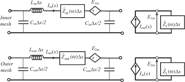
Figure 7.16 Π-type equivalent circuit of a coaxial cable section of length Δx
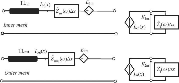
Figure 7.17 TL-type equivalent circuit of a coaxial cable section of length Δx
This last circuit has the great advantage of reducing the computational time, and it provides more accurate results. Note that it is consistent with the approach used in Figure 7.2 for discussing the loss effects on signals traveling down a line.
In order to implement the equivalent circuits of Figures 7.16 and 7.17 in any SPICE-based circuit simulator, the frequency-dependent impedances ![]() ,
, ![]() , and
, and ![]() need to be modeled by an equivalent RLC network which can be obtained by the vector fitting technique as described in the next section.
need to be modeled by an equivalent RLC network which can be obtained by the vector fitting technique as described in the next section.
7.2.1.3 SPICE Circuit Extraction by Vector Fitting
The Vector Fitting (VF) technique makes it possible to approximate any complex function of frequency by a rational polynomial expression in terms of poles and residues, as described in detail by Gustavsen and Semlyen [28]. A code implementing the VF procedure in Matlab is kindly provided by these authors and can be downloaded from the website http://www.energy.sintef.no/Produkt/VECTFIT/index.asp.
The derivation of the RLC network by VF can be shown for the case of a generic frequency-dependent impedance ![]() , which can be
, which can be ![]() ,
, ![]() , and
, and ![]() , by simply replacing the subscript ‘h’ with ‘in’, ‘out’, or ‘t’. By the VF procedure, Zh(ω) is expressed as
, by simply replacing the subscript ‘h’ with ‘in’, ‘out’, or ‘t’. By the VF procedure, Zh(ω) is expressed as

where N is the order of the approximating function, and Ahi and phi are the ith residue and pole respectively. By simple manipulations and by separating the contribution of the Nr real poles from those of the Nc couples of complex conjugate poles (i.e. N = Nr + 2Nc), Equation (7.67) can be written as

where the symbol * denotes a complex conjugate term and


Each real pole in Equation (7.68) can be modeled by an RL parallel circuit, as shown in Figure 7.18a, where the parameters are given by
Each complex conjugate pair enclosed in square brackets in Equation (7.68) can be modeled by the equivalent circuit of Figure 7.18b, where the parameters are defined as


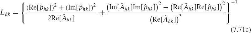


Figure 7.18 Equivalent circuits associated with (a) the ith real pole and (b) the kth complex conjugate pairs
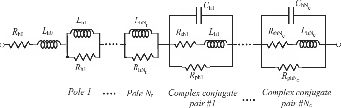
Figure 7.19 Equivalent circuit of the frequency-dependent impedance ![]()
where Re[.] and Im[.] are operators that allow the real and imaginary part of a complex number to be computed.
The equivalent circuit of impedance (7.68) is shown in Figure 7.19 and comprises the series connection of the following components:
- resistance Rh0;
- inductance Lh0;
- RL parallel circuits associated with the Nr real poles, the parameters of which are given by Equation (7.70);
- RLC circuits associated with the Nc conjugate pairs, the parameters of which are given by Equation (7.71).
In general, ![]() and
and ![]() are characterized by a magnitude increasing with frequency, and their polynomial approximations obtained by VF consist of real poles only. On the other hand, the transfer impedance of the shield presents a polynomial approximation according to Equation (7.68), including both real and complex conjugate pair poles.
are characterized by a magnitude increasing with frequency, and their polynomial approximations obtained by VF consist of real poles only. On the other hand, the transfer impedance of the shield presents a polynomial approximation according to Equation (7.68), including both real and complex conjugate pair poles.
At this point, after the VF procedure and circuit synthesis, the following observations can be made concerning the equivalent circuits obtained:
- The RLC parameters are constant irrespective of frequency, and are appropriate for making the circuit suitable for transient analysis.
- The circuit models of a cable section of length Δx shown in Figures 7.16 and 7.17 can be easily implemented in any circuit simulator in commerce, and the impedances
 ,
,  , and
, and  can be defined by suitable subcircuits added to the SPICE library.
 - The equivalent circuit models are suitable for radiated field computation, as they provide the current distribution along the cable shield.
- The models can be extended to the case of multiconductor cables such as twinax or shielded twisted-pair cables. The difficulty in this case is knowledge of the cable parameters. In fact, in the case of multiconductor cables, an analytical approach accounting for the proximity effect between the inner conductors is not available. For this reason, the p.u.l. parameters, including frequency-dependent losses, can be obtained by measurements or by numerical methods.
Some examples focused on signal integrity are provided below to show the validity and efficiency of the circuits described in Figures 7.16 and 7.17. A further application for predicting interference by an ESD event in an RG58 coaxial cable can be found elsewhere [36, 37]. Note that the procedure can be extended to other types of interconnect such as other cables and PCB traces.
Example 7.2: Signal Integrity in a Lossy Coaxial Cable
As an example, consider a coaxial cable having the following parameters: inner wire radius rc = 0.395 mm, internal shield radius rsi = 1.397 mm, external shield radius rse = 1.524 mm, dielectric relative permittivity εrd = 2.3, shield and wire conductivity σc = σs = 5.8 × 10⁷ Ω−1/m, vacuum permeability μ0 = 4π10−7 H/m, and vacuum permittivity ε0 = 8.854 × 10⁻¹² F/m. The calculation of the parameters of the equivalent circuit of the inner mesh of Figure 7.17 was performed adopting a cable segment of length Δx = 5 cm. The lossless transmission line TLin has a nominal characteristic impedance ![]() and a delay time
and a delay time ![]() , with Lin = 12.632 nH and Cin = 5.065 pF. The equivalent circuit of the frequency-dependent impedance
, with Lin = 12.632 nH and Cin = 5.065 pF. The equivalent circuit of the frequency-dependent impedance ![]() obtained by the VF procedure is shown in Figure 7.20, where the notation is that of the circuit simulator MicroCap [38] (the notation ‘.define X Y’ means that the number or variable Y is assigned to the variable X). This circuit was obtained by adopting 10 poles, which is an appropriate number to ensure accuracy in the frequency range of interest (0–10 GHz). Note that the series inductance L10 = Lin is not present in Figure 7.20 because it is included in TLin. The first resistance R1 = 2.244 mΩ is the DC resistance of the inner wire plus the shield. In order to generalize the circuit for an arbitrary length of cable section, the parameter dx = Δx is defined in Figure 7.20. The comparison between the impedance obtained by the circuit in Figure 7.20 and the impedance computed analytically using the previous equations based on skin depth for a coaxial cable is shown in Figure 7.21, where a very good agreement can be observed in the full range of interest.
obtained by the VF procedure is shown in Figure 7.20, where the notation is that of the circuit simulator MicroCap [38] (the notation ‘.define X Y’ means that the number or variable Y is assigned to the variable X). This circuit was obtained by adopting 10 poles, which is an appropriate number to ensure accuracy in the frequency range of interest (0–10 GHz). Note that the series inductance L10 = Lin is not present in Figure 7.20 because it is included in TLin. The first resistance R1 = 2.244 mΩ is the DC resistance of the inner wire plus the shield. In order to generalize the circuit for an arbitrary length of cable section, the parameter dx = Δx is defined in Figure 7.20. The comparison between the impedance obtained by the circuit in Figure 7.20 and the impedance computed analytically using the previous equations based on skin depth for a coaxial cable is shown in Figure 7.21, where a very good agreement can be observed in the full range of interest.
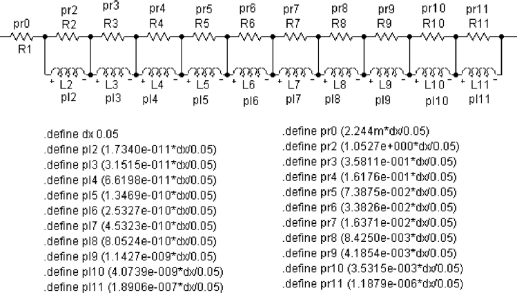
Figure 7.20 Equivalent circuit of impedance ![]() for a coaxial cable of generic length dx
for a coaxial cable of generic length dx
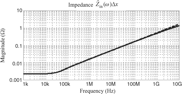
Figure 7.21 Magnitude of ![]() as a function of frequency: analytical computation (dashed line); equivalent circuit with 10 poles (solid line). Δx = 5 cm
as a function of frequency: analytical computation (dashed line); equivalent circuit with 10 poles (solid line). Δx = 5 cm
The scattering parameters of the coaxial cable of length l = 5 cm are shown in Figure 7.22, where the results obtained by the following four different circuit models are compared:
The cable is simulated as a four-port net where the p.u.l. parameters are computed by the previous equations, and S-parameters are obtained by the exact formulation described in Section 11.2.
Figure 7.22 S-parameters of a 5 cm long coaxial cable: analytical approach (solid line); one-cell model (dotted line); 10-cell model (dashed line); 100-cell model (dashed-dotted line)
- The cable is simulated with one cell (i.e. Δx = l = 5 cm) according to Figure 7.17, assuming E1m = 0, and using the equivalent circuit of Figure 7.20 to model .
- The cable is simulated with a cascade connection of 10 cells of length Δx = 0.5 cm.
- The cable is simulated with a cascade connection of 100 cells of length Δx = 0.05 cm.
In should be noted that only the cable model based on the cascade connection of 100 cells reveals a very good agreement in the calculation of the scattering parameter S11 up to 10 GHz. In fact, at 10 GHz the wavelength is λ = 300/fMHz = 300/10 000 = 0.03 m = 3 cm, and, to satisfy the electrically short condition on which the segmentation approach is based, the cable segment should be less than one-tenth of the wavelength, and therefore less than 0.3 cm. On the other hand, a very good agreement among the four models can be observed in the case of parameter S21. This has an important practical effect, as generally the interest is focused on data transmission at the end of the cable.
As a second application, an UltraWide Band (UWB) signal transmitted along an RG58 coaxial cable of 1.83 m length, matched at both ends, is considered. The UBW signal has a bandwidth of 3.1–6.5 GHz and is therefore suitable for testing the proposed skin-effect model based on the VF technique. To account suitably for this very high frequency content, the cable was modeled by a cascade connection of 610 cells of 0.3 cm length. In a theoretical lossless line, considering the partitioning effect between RS = Z0 and Z0, the signal ES/2 shown in Figure 7.23 is launched onto the coaxial cable and transmitted to the load without attenuation. In reality, the signal is attenuated by the skin effect. A very good agreement can be observed in Figure 7.23 between the voltage on the load VL obtained by the circuit model and the measurement performed on a LeCroy digital oscilloscope (Wavemaster 8600A).

Figure 7.23 Coaxial cable matched at both ends and modeled as a cascade of 610 cells including the skin effect: comparison between measured (dashed line) and computed (solid line) waveforms
7.2.2 Circuit Extraction of Twisted-Pair Cables
Twisted-pair cables are widely used in several applications for their capability to reduce EMI effects induced by external magnetic fields and crosstalk produced by parallel wires. In particular, unshielded twisted-pair (UTP) cables are involved in the realization of local area networks (LANs) connecting personal computers, workstations, etc. Owing to the continuous development of high-speed communication technology, UTPs are required to support signals propagating at frequencies up to some gigahertz.
Typically, UTPs comprise two dielectrically insulated copper wires twisted together inside a dielectric sheath. This means that the proximity effect plays an important role regarding losses. An analytical approach for calculating the cable simulation model like the one used for coaxial cables cannot be used for cables of this type. However, a circuit model can be built starting from the S-parameters computed numerically by a full-wave tool for an electrically short cable segment (see Section 11.2). S-parameters can be measured, but this is very difficult and almost impossible for a short segment of cable.
Once the scattering matrix ![]() is obtained by the full-wave simulation, it can be used to extract two different SPICE equivalent circuits:
is obtained by the full-wave simulation, it can be used to extract two different SPICE equivalent circuits:
- Π-type equivalent circuit;
- TL-based equivalent circuit.
Both circuits are derived by a different port representation of the cable, which can be easily derived by the scattering matrix. For instance, the impedance matrix ![]() is given by [39]
is given by [39]
where I is the identity matrix and zrif is the port normalization impedance.
7.2.2.1 Π-type Equivalent Circuit
The first UTP macromodel is the Π-type equivalent circuit shown in Figure 7.24a. The transversal and longitudinal admittances of this circuit can be obtained as [32], [39]


where ![]() and
and ![]() are the coefficients of the impedance matrix
are the coefficients of the impedance matrix ![]() defined by Equation (7.72), and ‘det’ stands for the matrix determinant. The VF procedure is applied to carry out a rational approximation for the frequency-dependent admittances
defined by Equation (7.72), and ‘det’ stands for the matrix determinant. The VF procedure is applied to carry out a rational approximation for the frequency-dependent admittances ![]() and
and ![]() , so that the generic admittance
, so that the generic admittance ![]() (with h = long or trasv) can be approximated by
(with h = long or trasv) can be approximated by

Figure 7.24 (a) Π-type equivalent circuit and (b) equivalent circuit of the frequency-dependent admittance ![]() with h = long or trasv
with h = long or trasv
where N is the order of the approximating function, and Ahi and phi are the ith residue and pole respectively. The rational function (7.74) can be easily modeled by an equivalent RLC network suitable for direct implementation in a CAD circuit simulator. To derive the equivalent circuit, let indicate Nr be the number of real poles and Nc the number of complex conjugate pairs, so that Equation (7.74) becomes

where the asterisk denotes a complex conjugate. The equivalent circuit associated with Equation (7.75) is shown in Figure 7.24b and is given by the parallel connection of the following branches:
- a conductance Gh0 = dh;
- a capacitance Ch0 = eh;
RL series circuits associated with Nr real poles, the parameters of which are
RLC circuits associated with the Nc complex conjugate pairs, the parameters of which are given by


It should be noted that the applied VF procedure makes it possible to ensure overall passivity of the admittances but not local passivity, as some negative components can be present in the SPICE circuit. This fact can bring instability in transient analysis when cascading a large number of cells.
7.2.2.2 TL-based Equivalent Circuit
To avoid instability problems and simplify the equivalent circuit of a section of the cable in order to speed up the simulation while reducing the number of circuit elements, the TL-based model shown in Figure 7.25a can be used. This model consists of three parts:
- A frequency-dependent impedance
 , which takes into account the skin and proximity effects and is computed using the analytical approach outlined in Sections 7.1.2 and 7.1.3.
 - A frequency-dependent admittance
 , which takes into account the dielectric effect and is computed using the analytical approach outlined in Section 7.1.4.
 - A lossless transmission line TLUTP associated with the section of cable under consideration. It includes the nominal p.u.l. inductance L0 and capacitance C0 used to characterize a lossless line. This can be done because the propagation coefficient and therefore the delay time is slightly dependent on the type of losses (see Figure 11.1).
The frequency-dependent impedance ![]() and admittance
and admittance ![]() can be modeled by RLC networks, which can be obtained by the VF procedure as discussed in the previous section.
can be modeled by RLC networks, which can be obtained by the VF procedure as discussed in the previous section.
A simplified TL-based model can be obtained by neglecting the effect of dielectric losses, and then by modeling the shunt admittance by the simple capacitance C0, the contribution of which is accounted for in the lossless line, as shown in Figure 7.25b.
Example 7.3: Signal Integrity in a Lossy UTP Cable
This example illustrates how to apply the Vector Fitting (VF) technique and the analytical models described in Section 7.1 in order to find a suitable equivalent circuit for a lossy UTP line. Consider the UTP cable having the structure shown in Figure 7.26 and described by the parameters reported in Table 7.2. The UTP configuration was modeled by the 3D full-wave numerical tool MicroWave Studio (MWS) based on the Finite Integration Technique [40]. The 3D model of the considered UTP cable is shown in Figure 7.26, where two pitches of the twist are considered. The simulation of a longer UTP involving several pitches would require a bigger simulation time owing to the increasing complexity. The two wires are modeled with copper material so that the internal losses are taken into account in the full-wave simulation.

Figure 7.25 (a) TL-based equivalent circuit and (b) simplified TL-based equivalent circuit

Figure 7.26 Structure of the UTP cable simulated by MWS
Owing to the fine details of the cable, a local subgrid was used in order to obtain accurate results with a reasonable computational effort. The simulations were carried out by exciting the UTP cable at the ports (i.e. cable terminations), adopting as the port impedance the characteristic impedance Z0 = 135.2 Ω of the cable computed by the code with its Time Domain Reflectometer (TDR) macro (see Section 11.1). It should be noted that this choice makes it possible to increase numerical accuracy and efficiency, leaving out multiple reflections.
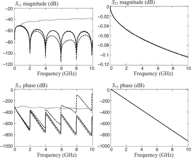
The VF procedure applied to the Π-type equivalent circuit of the cable under investigation leads to a good accuracy up to 5 GHz, adopting 10 poles: two real poles and four complex conjugate pairs.
The equivalent Π-type SPICE circuits as well as the equivalent circuits of the admittances ![]() and
and ![]() implemented into the MicroCap simulator are shown in Figure 7.27. The equivalent TL-based circuit is shown in Figure 7.28a, and the equivalent circuits of
implemented into the MicroCap simulator are shown in Figure 7.27. The equivalent TL-based circuit is shown in Figure 7.28a, and the equivalent circuits of ![]() and
and ![]() fitted by eight poles are shown in Figures 7.28b and 8.28c respectively. The decoupling capacitance of 1 pF was put in series with
fitted by eight poles are shown in Figures 7.28b and 8.28c respectively. The decoupling capacitance of 1 pF was put in series with ![]() to decouple the net in DC conditions. The parameters and equations required to define the TL-based circuit model are given in Tables 7.3, 7.4, and 7.5, with comments. It must be pointed out that the equivalent circuit of
to decouple the net in DC conditions. The parameters and equations required to define the TL-based circuit model are given in Tables 7.3, 7.4, and 7.5, with comments. It must be pointed out that the equivalent circuit of ![]() was obtained by applying vector fitting to the admittance
was obtained by applying vector fitting to the admittance ![]() , as Equation (7.27) was used and the nominal capacitance C0 (see Equation (7.28)) was extracted and included in the lossy line model. Another thing to consider is that the hypothetical UTP cable modeled as shown in Figure 7.26 had a low loss tangent tan θ. This explains why the onset frequency of the dielectric losses reported in Table 7.5 is so high. In any case, the purpose of this example is to compare the proposed equivalent circuits. In Example 7.4 the simulation of an actual UTP cable with experimental validation will be presented.
, as Equation (7.27) was used and the nominal capacitance C0 (see Equation (7.28)) was extracted and included in the lossy line model. Another thing to consider is that the hypothetical UTP cable modeled as shown in Figure 7.26 had a low loss tangent tan θ. This explains why the onset frequency of the dielectric losses reported in Table 7.5 is so high. In any case, the purpose of this example is to compare the proposed equivalent circuits. In Example 7.4 the simulation of an actual UTP cable with experimental validation will be presented.
Table 7.2 Geometrical parameters of the simulated UTP cable
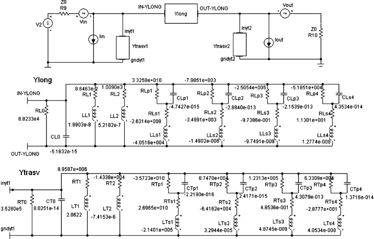
Figure 7.27 Π-type model and equivalent circuits of the admittances ![]() and
and ![]() of the UTP cable of Figure 7.26 implemented in the MicroCap simulator
of the UTP cable of Figure 7.26 implemented in the MicroCap simulator
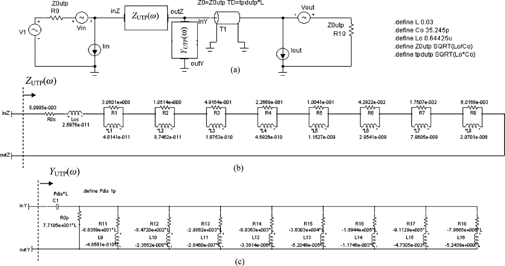
Figure 7.28 SPICE equivalent circuit of the TL-based model of the UTP cable of length l = 3 cm: (a) equivalent circuit to compute S-parameters; (b) equivalent circuit of ![]() accounting for skin and proximity effects; (c) equivalent circuit of conductance
accounting for skin and proximity effects; (c) equivalent circuit of conductance ![]() associated with the dielectric effect. The contribution of L0 and C0 are included in the lossless transmission line model
associated with the dielectric effect. The contribution of L0 and C0 are included in the lossless transmission line model
Table 7.3 General UTP parameters used for computation

The impedances of the TL-based model computed with the parameter values and formulae of Tables 7.3–7.5 are shown in Figure 7.29. The magnitude of the impedance ![]() representing the losses in closed-form expression by Equation (7.17) is perfectly consistent with the result produced by the equivalent circuit in Figure 7.28b. As regards the phase, there are some slight non-significant differences around the value of 45°, as expected when the amount of the real part equals the imaginary part. The results produced by three different possible representations of the admittance
representing the losses in closed-form expression by Equation (7.17) is perfectly consistent with the result produced by the equivalent circuit in Figure 7.28b. As regards the phase, there are some slight non-significant differences around the value of 45°, as expected when the amount of the real part equals the imaginary part. The results produced by three different possible representations of the admittance ![]() are also compared in Figure 7.29:
are also compared in Figure 7.29:
- simplified model based on C0 only (no dielectric losses);
- analytical formulation taking into account dielectric losses;
- equivalent circuit coming from the VF technique.
The results produced by the three different models are in very good agreement both for the magnitude and the phase, which is always −90° in the whole frequency range.
Table 7.4 UTP parameters used to calculate skin and proximity effects
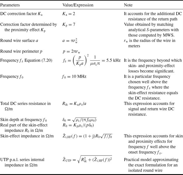
It should be noted that, while many of the parameters in Tables 7.3–7.5 are set considering the geometric and electric characteristics of the UTP cable considered, generally the parameters Kp and θ0, related to the proximity and dielectric effects respectively, are unknown a priori and can be computed by matching the S-parameters calculated using the closed-form expressions presented in Section 7.1 with those computed by MWS. In many practical cases, such as traces in a PCB and commercial cables, θ0 is known while Kp must be determined. The frequency-domain scattering parameters for the UTP cable under investigation are shown in Figure 7.30. While the magnitudes S21 are very close in the full frequency range, the magnitudes S11 show large differences above 1.5 GHz. However, this is not very important from a practical viewpoint because S21 represents the transfer function of the cable while S11 represents the reflections at the source end. In data transmission the interest is mainly focused on the waveforms of the signals transmitted to the load to obtain the eye diagram. Remember that in a lossless line S11 = 0 and S21 = 1. To support this statement, some validation of the models will be given below.
Table 7.5 Parameters used to account for the dielectric effect in the UTP cable

The scattering parameters obtained by the Π-type equivalent circuit in Figure 7.24, by the TL-based model in Figure 7.25a, and by the simplified TL-based model in Figure 7.25b are compared with those computed by MWS in Figure 7.31, and the following observations can be made:
The Π-type model reproduces very well the parameter S11 computed by MWS both in magnitude and in phase in the whole frequency range of interest, while the magnitude of S21 is slightly different above 1.5 GHz. A point of resonance appears for both S-parameters at about 3.5 GHz. This resonance is also present in the admittances
 and
and  computed by Equation (7.73) using the S-parameters obtained by MWS. The discrepancies above 1.5 GHz are mainly due to the fact that the 3 cm cable segment is not electrically short at frequencies above 1 GHz, while the simulation extends up to 5 GHz. At 1 GHz the wavelength is λ = 30 cm and the segment to be electrically short should be less than λ/10. However, in building up the circuit model, it is necessary to compromise between accuracy and the need to limit the number of cells in cascade representing the line in order to save computer memory and to speed up the simulation.
Figure 7.29 Magnitude and phase of the impedance
and  of the UTP cable of length l = 3 cm. The lines used for representing ZUTP(ω) are the analytical expression (solid line) and the SPICE circuit (dashed line). Those used for representing are the analytical model (solid line), the SPICE circuit (dashed line), and the simplified C0 model (dotted line)
The TL-based model in Figure 7.25a provides an S21 parameter very close to the one obtained by MWS both in magnitude and phase. The magnitude of S11 increases with frequency and has a profile close to the peak values of S11 computed by MWS. The phase of S11 is different from that computed by MWS. However, as will be shown later by validation tests, this fact does not compromise the time-domain results.
Figure 7.30 S-parameters of the UTP cable computed by MWS (solid line) and obtained by closed-form equations (dashed line)
Figure 7.31 S-parameters of the UTP cable: MWS (solid line); Π-type circuit model (dotted line); TL-based model (dashed line); simplified TL-based model (dashed-dotted line)

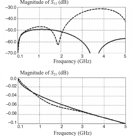

The differences between the Π-type circuit and the TL-based model in the time domain are shown in Figure 7.32. Simulations were performed for a point-to-point UTP interconnect of 3 m length and having the structure of Figure 7.1. Two conditions were simulated: the line matched at both ends, and the line mismatched at the source and load ends. For both models, 100 cells of 3 cm length were used to simulate the UTP cable. The line was excited by a step source of 2 V amplitude with a rise time tr = 0.5 ns. In matched conditions, both models give similar results and reproduce the typical source and voltage waveforms of a lossy line as depicted in Figure 7.3. The Π-type model presents some slight signal distortions owing to the fact that the cell of this model consists of three complex lumped-element nets. In mismatched conditions, distortions on the signal waveforms are again present, and some slight differences in delay time can be observed.
Although the Π-type model seems to provide closer S-parameters in magnitude and phase to the numerically computed waveforms in the full frequency range, except at the resonance frequency point, it could cause instability in transient simulation, especially when the number of cells in cascade is too large. For this reason, and considering the complexity of the nets, the Π-type circuit is not recommended. It could be used when the highest frequency of interest makes it possible to avoid resonance points and fewer cells are used. The TL-based model has the great advantage over the Π-type circuit that the simulations run in a few seconds instead of several minutes.

Figure 7.32 Simulated voltages at input VS and output VL of the UTP cable: (a) matched source and load conditions (RS = RL = Z0); (b) mismatched conditions (RS = Z0/10 and RL = Z010). Π-type circuit (dashed line) and TL-based model (solid line)
The accuracy of the VF technique applied to the TL-based model is also proven by comparing the results with those obtained by the IFFT of the exact AC analytical model of lossy TLs outlined in Section 7.1.5.2, and indicated here as the AC-IFFT model. Referring to Table 7.1, the following parameters where used for the IFFT: m = 14, Δt = 0.05 ns, τ = 1 ns, tr = 0.5 ns. The cable parameters are those given in Tables 7.3–7.5. The results are shown in Figure 7.33, where a very good agreement can be observed.
As a further validation of the TL-based model, an UTP cable of 90 cm length (60 pitches) was manually constructed, and 30 cells were used to perform the transient simulation of the UTP cable terminated at both ends with 50 Ω resistances. The cable was excited with a unit step voltage source of 2 V amplitude with a rise time tr = 0.25 ns. The transient input and output voltages are shown in Figure 7.34, where a good agreement between simulations and measurements can be observed. The slight oscillations in the measured waveforms are due to the non-uniformity of the twisted-pair wires used for the experiment.

Figure 7.33 Simulated voltages at input VS and output VL of the UTP cable in matched source and load conditions. TL-based circuit model (dashed line) and AC-IFFT model (solid line)
Figure 7.34 Simulated and measured voltages at input VS and output VL of the UTP cable in matched source and load conditions. Measurements (dashed line) and TL-based circuit model (solid line)
7.3 Modeling Lossy Lines in the Time Domain by the Scattering Parameters Technique
The technique described in this section should be applied to the case of long cables when the segmentation technique becomes too expensive in terms of the number of cells to be put in cascade. The main advantage of this approach is that the model is independent of the cable length.
Consider a cable representing a transmission line with nominal characteristic impedance ![]() and time delay TD = tpdl, where tpd is the per-unit-length propagation delay time of the cable and l is the cable length. As practical cables of interest have electrically short dimensions in the transversal section, the cable can be considered as a two-port network described by the generalized scattering parameters which are linked to the voltages and currents at the line ends as shown in Figure 7.35. The incident (a1, a2) and reflected (b1, b2) waves can be calculated from the voltages and the currents at both ends of the line using the normalizing factor
and time delay TD = tpdl, where tpd is the per-unit-length propagation delay time of the cable and l is the cable length. As practical cables of interest have electrically short dimensions in the transversal section, the cable can be considered as a two-port network described by the generalized scattering parameters which are linked to the voltages and currents at the line ends as shown in Figure 7.35. The incident (a1, a2) and reflected (b1, b2) waves can be calculated from the voltages and the currents at both ends of the line using the normalizing factor ![]() , where Z0 is the cable nominal characteristic impedance. The following equations hold in both the frequency and the time domains:
, where Z0 is the cable nominal characteristic impedance. The following equations hold in both the frequency and the time domains:

Figure 7.35 Incident and reflected waves applied to a transmission line seen as a two-port network
By a demonstration similar to that given by Paul [24] to obtain the Branin circuit presented in Section 5.2.6, it can be shown that the TL described by Equations (7.78) and (7.79) can be modeled by the equivalent circuit of Figure 7.36, where
In order to define the equivalent circuit of Figure 7.36, it is necessary to find suitable expressions for the voltage sources (7.80), taking into account frequency-dependent losses. To this end, let us start with the representation of a lossy TL in the frequency domain by the S-parameters:


Figure 7.36 Equivalent circuit of a transmission line, using the concept of reflected waves
Note that the off-diagonal coefficient in Equation (7.81) is written by extracting the term related to the time delay, or equivalently to the phase constant. In this way, the two main contributions associated with the line propagation delay and with the frequency-dependent losses are separately highlighted, which is reasonable, as the TL propagation coefficient is slightly dependent on types of loss, as was shown in Figure 7.11.
In practice, the following relations hold: ![]() and
and ![]() . By definition, the off-diagonal coefficient
. By definition, the off-diagonal coefficient ![]() in Equation (7.81) represents the TL transfer function, while the diagonal terms represent the reflections at the line ends.
in Equation (7.81) represents the TL transfer function, while the diagonal terms represent the reflections at the line ends.
Moving (7.81) to the time domain yields

The right-hand side of Equation (7.82) contains convolution integrals that must be solved numerically to compute the dependent voltage sources ei(t) and eo(t) defined by Equations (7.80). From the definition of incident waves, and with the current notation introduced in Figure 7.36, we have

Finally, by using Equations (7.82) and (7.83), the dependent voltage sources (7.80) at each time instant are calculated as the sum of two convolution integrals between the S-parameters and the algebraic combination of voltages and currents at the line ends.
In the case of a lossless TL matched at both ends, the S-parameters are
S12 = S21 = 1
S11 = S22 = 0
In this case, Equation (7.84) coincides with Equation (5.22), and therefore the equivalent circuit of Figure 7.36 is equivalent to the Branin circuit introduced in Chapter 5 to model lossless TLs and present in the SPICE library.
The time-domain S-parameters necessary to calculate the convolution integrals in Equation (7.82) can be obtained as the response of a narrow Gaussian pulse for the frequency range of interest, and this can be done by full-wave numerical tools (i.e. MWS based on the FIT technique), or by measurements according to the set-up shown in Figure 7.37, where the TL is excited by a step generator. The rise time of the step generator should be fast enough to obtain the waveforms of Figure 7.3. Moreover, as in practice both the step generator and the oscilloscope have an internal resistance equal to the standard 50 Ω value, to match the TL at both ends, two resistances of value R = Z0 − 50 Ω are required.
The S-parameters to be used in the convolutions (7.82) are related to the voltages VS and VL at the line ends (see Figure 7.37) by
In summary, the computation of ei(t) and eo(t) in the lossy TL circuit model of Figure 7.36 must be performed by the following operations:
- Numerical derivative of the voltage step responses of the matched line to calculate by Equations (7.85) the time-domain scattering parameters S11(t) and S21(t).
- Numerical convolution integral between scattering parameters S11(t) and S21(t) and incident waves a1(t) and a2(t) according to Equation (7.82). The incident waves are functions of the voltages and currents at opposite ends, as stated by Equations (7.80).
- When performing convolution with S12 = S21, the incident waves must be delayed by a time TD, as shown in Equation (7.82).
The main problem in implementing the lossy TL circuit model of Figure 7.36 is related to the convolution, as many SPICE-like simulators do not offer this feature. However, popular commercial mathematical codes such as MathCad or Matlab can be used with success, as shown by the following examples.

Figure 7.37 Set-up to measure the S-parameters in the time domain
Example 7.4: Eye Diagram of a 75 m Unshielded Twisted-pair Cable Driven by an RS422 Device
To validate the model with experimental results, the test set-up shown in Figure 7.38 is considered. The cable is a twisted-pair cable of Cat.5e and length l = 75 m. The driver is a differential CMOS 34C87 device and the receiver is a 34C86 device (RS422 standard). The data stream is an NRZ sequence at 32 Mb/s. The line is terminated with three resistances having the task of partially matching the line, and of ensuring polarization of the receiver when the cable is disconnected, as often required in practice.
As the interest is focused on the eye diagram, and the driver output characteristic is symmetric, the simulation can be performed by the equivalent circuit of the interconnect shown in Figure 7.38. The driver swings from −3 V to 3 V and has an output resistance RS = 10 Ω. The line has a differential characteristic impedance Z0 = 100 Ω, a p.u.l. propagation delay time tpd = 5 ns/m, and a total DC resistance Rdcl. The load resistance RL is assumed to be the parallel connection between 150 Ω and 2 kΩ, because in AC condition the ground and the power pins of the receiver are at the same potential.
The waveform in Figure 7.3, suitable for computing S-parameters in the time domain, can be obtained in two ways:
- by measurements according to the set-up shown in Figure 7.37 if the sample of cable is available;
- by the analytical approach outlined in Section 7.1, considering the typical electrical characteristic of an UTP Cat.5e cable as reported by Johnson and Graham [25] (see Table 8.2 for tan θ and Table 8.3 for Kp).
In this second case, the main cable parameters of Tables 7.3–7.5 are set as follows: rw = 0. 2285 mm (wire radius), ν0 = 0.7c = 2.099 × 10⁸ m/s, l = 75 m, Z0 = 100 Ω, f0 = 10 MHz, θ0 = 0.0115, Ka = 2, and Kp = 2.7. These parameters give fδ = 46 kHz and fθ = 203 MHz. The dielectric losses become significant over 200 MHz. The input and output waveforms computed by the AC-IFFT model are shown in Figure 7.39, where the voltage on the load is shown without the delay TD = ν0l for plot representation. The final voltages VS∞ = 1.073 V and VL∞ = 0.927 V are also indicated. For clarity, only the significant parts of the waveforms are shown. A very good agreement can be observed between measured and predicted waveforms by the AC-IFFT model, which shows the efficiency of the analytical approach for long cables. Therefore, in the absence of a cable sample having the length of interest, the S-parameters can be estimated in the time domain by matching the frequency-domain S-parameters calculated by the closed-form analytical approach with those computed by a full-wave code for an electrically short segment of cable, as outlined in Section 7.2.1.
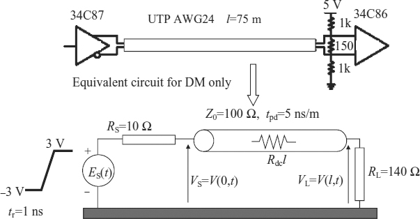
Figure 7.38 Point-to-point interconnect with differential driver/receiver devices and its equivalent circuit for differential mode signaling

Figure 7.39 Input and output voltages of the UTP Cat-5e cable of 75 m length matched at both ends according to the set-up of Figure 7.3: measured (dashed line) and computed by the AC-IFFT (solid line)
The simulated waveforms when the line is sourced with a non-return to zero (NRZ) sequence of bits with a data rate of 32 Mb/s are shown in Figure 7.40. The convolution integrals were performed starting from the measured voltages in Figure 7.39. Very similar results can be obtained using the computed S-parameters. The comparison between waveforms obtained by a lossless model and those obtained by a lossy line model is quite interesting. Significant discrepancies can be observed, especially for the voltages on the load VL. The lossy model is validated by comparison between simulated and measured waveforms using the eye diagram representation as shown in Figure 7.41 for the voltage on the load. Very good agreement can be observed, although the sequence of bits used for simulation is shorter than the measured one.

Figure 7.40 Input and output voltages of the UTP Cat-5e cable of 75 m length matched at both ends and excited by a NRZ sequence of bits at 32 Mb/s: TL lossless model (dashed line) and TL lossy model (solid line)

Figure 7.41 Eye diagrams of the voltage on the load for the 75 m Cat-5e UTP cable with a NRZ sequence of 32 Mb/s
Example 7.5: Coaxial Cable Driven by an Ultrawide-band Signal Simulated by the TL Model Based on the Time-domain S-parameters
As a further validation of the lossy TL model based on the time-domain S-parameters, the same coaxial cable driven by the UWB signal as that used in Example 7.2 is considered. To perform simulations, the following steps are required:
- Find the equivalent circuit of an electrically short section of cable by the VF technique; in this case Δx = 3 mm is suitable, as in Example 7.2.
- Run the simulation of the cable equivalent circuit obtained by cascading 610 cells, and adopting matching conditions at both the cable ends.
- Calculate by Equation (7.85) the time-domain S-parameters necessary to implement the convolution integrals of the dependent sources ep(t) and ea(t) in Figure 7.36.
All these steps are illustrated in Figure 7.42. It is necessary to point out that S11step(t) = VS(t) − ESo and S21step(t) = VL(t) must be computed adopting a time interval small enough to avoid numerical attenuation effect. In the proposed example, Δt = 0.01 ns is used, as the rise time of the step source is tr = 0.1 ns. Comparison between simulated and measured waveforms of the load voltage is shown in Figure 7.43.
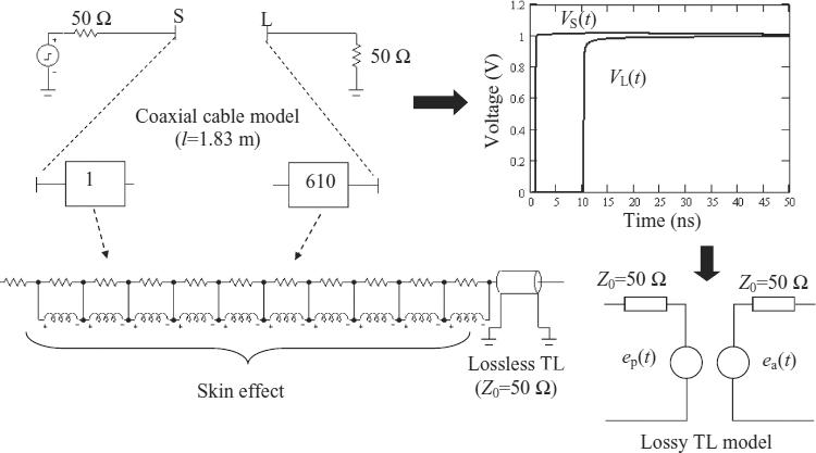
Figure 7.42 Computed input and output voltages of the coaxial cable by 610 cells of length Δx = 3 mm to be used with the lossy TL model based on the time-domain S-parameters

Figure 7.43 Coaxial cable matched at both ends and modeled as a simple network based on S-parameters in the time domain: comparison between measured (dashed line) and computed (solid line) waveforms
7.4 Conclusions
To conclude this section, it is possible to make the following observations:
- The two approaches outlined for simulating lossy TLs in the time domain, Vector Fitting (VF) and time-domain S-parameters, are suitable for modeling several structures such as traces on PCBs (microstrips, striplines) and cables (coaxial, twinax, UTP, SFTP), once the Z-, Y-, or S-parameters of an electrically short segment of cable are known.
- The VF method requires knowledge of the Z- and Y-parameters of an electrically short section of the line. These circuit parameters can be obtained by analytical expressions when available (e.g. coaxial cables), or by numerical computations of S-parameters in the frequency domain in order to consider losses such as skin, proximity, and dielectric effects. The equivalent circuit of the cable section reproducing the computed S-parameters can be easily implemented in any SPICE-like simulator and is suitable for performing simulations directly in the time domain. It has been demonstrated that each cell can be simulated by a Π-type model, or better by a TL-based model where a lossless TL is extracted and two networks for Z and Y are used to model frequency-dependent losses. This modeling procedure can be useful for short lossy TLs inserted in a general topology of interconnect structures when the required number of cells for each line is not too large.
- The S-parameters method in the time domain requires knowledge of the time-domain S-parameters for the full length of the line. These parameters can be obtained by TDR-like measurements or by a SPICE-like simulator, using the models produced by the VF technique. The great advantages of this model are its simplicity in terms of circuit elements and its independence from the length of the line. It can be easily implemented in a mathematical code for point-to-point interconnect or in a SPICE-like simulator for general interconnect structures once a numerical convolution in the time domain is performed by the mathematical or chosen circuit-based simulation code. The model can also be used to simulate even and odd modes of propagation by using the circuit model presented in Section 6.2 [30].
When a sample of cable to be simulated with the length of interest is not available for measuring the time-domain S-parameters, the following procedure can be used:
- The S-parameters of an electrically short segment of cable are numerically calculated by full-wave simulations.
- The S-parameters calculated by the TL-based model are matched with those numerically computed, by varying the coefficients for proximity (Kp) and dielectric (tanθ) (when unknown) effects, until an acceptable approximation is obtained.
- The time-domain S-parameters of the line are found for the length of interest as the response of a step source performing simulation in the frequency domain and using the IFFT to obtain time-domain results (AC-IFFT model).
- Simulations of the interconnect structure are performed by the model of the lossy TL based on the computed time-domain S-parameters with a code that allows numerical derivative, convolution integral, and delay functions.
References
[1] Weeks, W., Wu, L., McAllister, M., and Singh, A., ‘Resistive and Inductive Skin Effect in Rectangular Conductors’, IBM Journal of Research and Development, 23 (6), November 1979, pp. 652–660.
[2] Gruodis, A., ‘Transient Analysis of Uniform Resistive Transmission Lines in a Homogeneous Medium’, IBM Journal of Research and Development, 23 (6), November 1979, 675–681.
[3] Gruodis, A. and Chang, C., ‘Coupled Lossy Transmission Line Characterization and Simulation’, IBM Journal of Research and Development, 25 (1), January 1981, 25–41.
[4] Yen, C.-S., Fazainc, Z., and Wheeler, R., ‘Time-domain Skin-effect Model for Transient Analysis of Lossy Transmission Lines’, Proceedings of the IEEE, 70 (7), July 1982, 750–757.
[5] Yen, C.-S., ‘Distribution and Equalization of Signal on Coaxial Cables used in 10 Mbit/s Baseband Local Area Network’, IEEE Trans. on Communication, 31 (10), October 1983, 1181–1186.
[6] Djordjevic, A., Sarkar, T., and Harrington, R., ‘Time-domain Response of Multiconductor Transmission Lines’, Proceedings of the IEEE, 75 (6), June 1987, 743–764.
[7] Chang, C.S., ‘Electrical Design of Signal Lines for Multilayer Printed Circuit Boards’, IBM Journal of Research and Development, 32 (5), September 1988, 647–657.
[8] Deutsch, A. et al, ‘High-speed Signal Propagation on Lossy Transmission Lines’, IBM Journal of Research and Development, 34 (4), July 1990, 601–615.
[9] Barr, A., ‘Calculation of Frequency-dependent Impedance for Conductors of Rectangular Cross Section’, AMP Journal of Technology, 1, November 1991, 91–100.
[10] Djordjevic, A. and Sarkar, T., ‘Closed-form Formulas for Frequency-dependent Resistance and Inductance per Unit Length of Microstrip and Strip Transmission Lines’, IEEE Trans. on Microwave Theory and Techniques, 42 (2), February 1994, 241–248.
[11] Deutsch, A., ‘Electrical Characteristics of Interconnections for High-performance Systems’, Proceedings of the IEEE, 86 (2), February 1998, 315–357.
[12] Antonini, G., Orlandi, A., and Paul, C., ‘Internal Impedance of Conductors of Rectangular Cross Section’, IEEE Trans. on Microwave Theory and Techniques, 47 (7), July 1999, 979–985.
[13] Ruehli, A. and Cangellaris A., ‘Progress in the Methodologies for the Electrical Modeling of Interconnects and Electronic Package’, Proceedings of the IEEE, 89 (5), May 2001, 740–771.
[14] Achar, R. and Nakhla, M., ‘Simulation of High-speed Interconnects’, Proceedings of the IEEE, 89 (5), May 2001, 693–728.
[15] Deutsch, A. et al, ‘On-chip Wiring Design Challenges for Gigahertz Operation’, Proceedings of the IEEE, 89 (4), April 2001, 529–555.
[16] Coperich, K., Morsey, J., Okhmatovski, V., Cangellaris, A., and Ruehli, A., ‘Systematic Development of Transmission-line Models for Interconnects with Frequency-dependent Losses’, IEEE Trans. on Microwave Theory and Techniques, 49 (10), October 2001, 1677–1685.
[17] Antonini, G., Drewniak, J., Orlandi, A., and Ricchiuti, V., ‘Eye pattern evaluation in high-speed digital systems analysis by using MTL modeling’, IEEE Trans. on Microwave Theory and Techniques, 50 (7), July 2002, 1807–1815.
[18] Elfadel, I., Huang, H.-M., Ruehli, A., Dounavis, A., and Nakhla, M., ‘A Comparative Study of Two Transient Analysis Algorithms for Lossy Transmission Lines with Frequency-dependent Data’, IEEE Trans. on Advanced Packaging, 25 (2), May 2002, 143–153.
[19] Coperich Branch, K., Morsey, J., Cangellaris, A., and Ruehli, A., ‘Physically Consistent Transmission Line Models for High-speed Interconnects in Lossy Dielectric’, IEEE Trans. on Advanced Packaging, 25 (2), May 2002, 129–135.
[20] Grivet-Talocia, S., Huang, H.-M., Ruehli, A., Canavero, F., and Elfadel, I., ‘Transient Analysis of Lossy Transmission Lines: an Efficient Approach Based on the Method of Characteristics’, IEEE Trans. on Advanced Packaging, 27 (1), February 2004, 45–56.
[21] ‘Data Transmission Lines and Their Characteristics’, AN-806, National Semiconductor, April 1992. Available online: www.national.com.
[22] ‘Long Transmission Lines and Data Signal Quality, National Semiconductor, AN-808, March 1992. Available online: www.national.com.
[23] Ramo, S., Whinnery, J., and Van Duzer, T., ‘Fields and Waves in Communication Electronics’, 3rd edition, John Wiley & Sons, Inc., New York, NY, 1994.
[24] Paul, C., ‘Introduction to Electromagnetic Compatibility’, John Wiley & Sons, Inc., Hoboken, NJ, 2006.
[25] Johnson, H. and Graham, M., ‘High-speed Signal Propagation: Advanced Black Magic’, Pearson Education, Inc., Prentice Hall PTR, Upper Saddle River, NJ, 2003.
[26] Gupta, K.C., Garg, R., Bahl, I., and Bhartia, P., ‘Microstrip Lines and Slotlines’, Artech House, Norwood, MA, 1996.
[27] Araneo, R., Celozzi, S., and Maradei, F., ‘Digital Signal Transmission through Differential Interconnects: Full-wave vs. Spice Modeling’, IEEE 2003 International Symposium on Electromagnetic Compatibility, Boston, MA, 18–22 August 2003, 855–858.
[28] Gustavsen, B. and Semlyen, A., ‘Rational Approximation of Frequency Domain Responses by Vector Fitting’, IEEE Trans. on Power Delivery, 14 (3), July 1999, 1052–1061.
[29] Caniggia, S. and Maradei, F., ‘Equivalent Circuit Models for the Analysis of Coaxial Cables Immunity’, IEEE 2003 International Symposium on EMC, Boston, MA, 18–22 August 2003, 881–886.
[30] Caniggia, S., ‘EMC Design of Digital Systems Using Macromodelling Procedures for Integrated Circuits and their Interconnections’, 5th Symposium and Technical Exibition on EMC, Zurich, 3–5 March 1983, 465–470.
[31] Caniggia, S. and Maradei, F., ‘SPICE-like Models for the Analysis of the Conducted and Radiated Immunity of Shielded Cables’, IEEE Trans. on Electromagnetic Compatibility, 46 (4), November 2004, pp. 606–616.
[32] D'Amore, M., ‘Electromagnetic Compatibility’ (in Italian), Edizioni Scientifiche Siderea, Rome, Italy, 2003.
[33] Vance, E., ‘Coupling to Shielded Cable’, John Wiley & Sons, Inc., New York, NY, 1978.
[34] Tesche, F., Ianoz, M., and Karlsson, T., ‘EMC Analysis Methods and Computational Models’, John Wiley & Sons, Inc., New York, NY, 1997.
[35] Tsaliovich, A., ‘Cable Shielding for Electromagnetic Compatibility’, Chapman and Hall, New York, NY, 1995.
[36] Caniggia, S. and Maradei, F., ‘Circuit and Numerical Modeling of ESD Coupling to Shielded Cables’, EMC Europe 2004 – International Symp. on Electromagnetic Compatibility, Eindhoven, The Netherlands, 6–10 September 2004.
[37] Caniggia, S. and Maradei, F., ‘Circuit and Numerical Modeling of Electrostatic Discharge Generators’, IEEE Trans. on Industry Applications, 42 (6), November/December 2006, 1350–1357.
[38] www.spectrum-soft.com.
[39] Young, B., ‘Digital Signal Integrity: Modeling and Simulation with Interconnects and Packages’, Prentice Hall PTR, Upper Saddle River, NJ, 2001.
[40] www.cst.com.
Signal Integrity and Radiated Emission of High-Speed Digital Systems Spartaco Caniggia and Francescaromana Maradei
© 2008 John Wiley & Sons, Ltd