
2
High-Speed Digital Devices
For many calculations or simulations of Signal Integrity (SI) and Radiated Emission (RE) effects, it is very important to know the input/output (I/O) static and dynamic characteristics of digital devices. The aim of this chapter is to highlight the basic characteristics of the main logic families: Transistor–Transistor Logic (TTL), Complementary Metal Oxide Semiconductor (CMOS) logic, and Emitter-Coupled Logic (ECL). The intention is to provide a background to understand the latest development of components for high-speed applications. How to build up a linear or a simple behavioral model that takes into account the non-linear effects of the driver and receiver is outlined. This must also be considered a starting point for building up more accurate behavioral models. The chapter ends with an introduction of the IBIS models. IBIS is a standard for a fast and accurate behavioral method for modeling I/O buffers based on I/V curve data derived from measurements or full-circuit simulations. An example is given of the use of this type of model by SPICE.
2.1 Input/Output Static Characteristic
In this section the main parameters of the digital technologies are presented to find out the I/O static characteristics of a device. The objectives of the component manufacturers are to improve speed by minimizing the transistor size and to decrease the power consumption by lowering the value of the voltage supply. Other modifications to improve the performance of the components are introduced at the circuit level, but the general behavior of the static characteristics remains the same. The reader can find more detailed information by consulting textbooks [1–3] and the numerous Application Notes (ANs) prepared by device manufacturers that are available on the web [4–18].
2.1.1 Current and Voltage Specifications
For good signal transmission in digital communication, the high-level current IOH sourced and the low-level current IOL sunk by the driver must in absolute value be less than the fixed values IOHmax and IOLmax given by the data sheet in a specified range of power supply and temperature (see Figure 2.1). As will be explained in Section 2.1.4, in the case of ECL devices, the current is sourced by the device for both logic levels. Under these conditions, a high-level voltage VOH ≥ VOHmin or a low-level voltage VOL ≤ VOLmin is guaranteed at the output of the driver. In this case, the worst-case static immunity at the high and low levels (i.e. NMHmin = VOHmin − VINmin and NMLmin = VILmax − VOLmax respectively) is preserved. On the other hand, for good driver capability, IOHmax and IOLmax should be much higher than the values specified for typical logic gates used for short interconnects in order to ensure static noise immunity and therefore switching of the receivers at the first step. This is a very important requirement, especially in the case of interconnects with distributed loads such as chain and bus structures with Thévenin termination (see Section 5.4).

Figure 2.1 Static noise immunity of an IC device: (a) driver D at low level and (b) at high level; (c) noise margin definition
The non-linear I/O static characteristics of IC digital devices (see Figure 2.2) are very useful for calculating reflections and crosstalk in interconnects simulated as transmission lines. The key line parameters are: the per-unit-length propagation delay time, tpd, and the characteristic impedance, Z0. Once the static output characteristics of the driver associated with the low and high levels are known by measurements, by SPICE simulations, or by data sheet, the output impedances of the device, ROL and ROH for low and high levels respectively, can be determined as the slope of the line passing through the current–voltage points of interest (IOL, VOL) and (IOH, VOH) as 1/RO = ΔIO/ΔVO. The voltage source EO associated with a determined RO is the intersection between the line passing from the point (IO, VO) with slope 1/RO and the voltage axis (i.e. line IO = 0). Therefore, the two values EO and RO change according to the location of the point (IO, VO), and to the output low or high level. The same considerations apply to the input parameters of the receiver, EI and RI. Usually, three or four regions in the driver output static characteristic can be recognized where EO and RO can be considered constant, as will be shown in the next sections. This is an advantage in building appropriate simple models of IC devices, as will be illustrated in Chapters 5 and 6. As a designer generally wishes to maximize the signal launched onto the line to cause switching of the receivers at the first step, the regions useful for data transmission are those with low RO. The current and voltage couple in the static condition is defined by the intersection between the receiver input and the driver output characteristics for both logic levels.
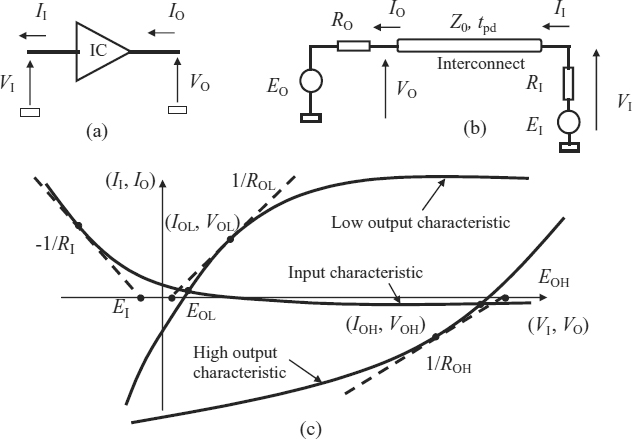
Figure 2.2 Voltage and current convention for (a) IC device and (b) interconnect. (c) Input and output static characteristics
Although there are many families of digital devices based on different technologies, they can be divided roughly into three broad categories:
- Transistor–Transistor Logic (TTL);
- Complementary Metal Oxide Semiconductor (CMOS) logics;
- Emitter-Coupled Logic (ECL).
TTL and ECL are bipolar technologies differing in implementation techniques, while CMOS (MOS technology) differs in fundamental transistor structure and operation. In the next sections, the static output characteristics of these categories of digital devices will be introduced and discussed with the purpose of building suitable simple circuit models for reflection and crosstalk predictions by the graphical method (see Chapter 5) or by SPICE-like circuit simulators.
2.1.2 Transistor–Transistor Logic (TTL) Devices
The designation ‘bipolar’ essentially refers to the basic component used to build this family of integrated circuits, the bipolar transistor [1]. Employing a bipolar transistor in the output driver of a logic function as well as the input buffer results in a Transistor-to-Transistor Logic (TTL) direct connection. Older technologies were interconnected via passive components such as resistors or diodes. Since the original TTL design, several enhancements have been employed to reduce power and to increase speed [17, 18]. Common to these has been the use of Schottky diodes, which, ironically, no longer strictly result in TTL connections. Consequently, the two names, Schottky and TTL, are used in combination: Low-power Schottky (LS), Advanced Low-power Schottky (ALS), and Advanced Schottky FAST TTL. Typical input and output stages of a TTL device are shown in Figure 2.3.
For a long time the superior characteristics of TTL compared with CMOS have been its relatively high speed and high output capability to drive long interconnects; these advantages are rapidly diminishing, as described in the next section. One family of devices, Advanced BiCMOS Technology (ABT), utilizes TTL circuitry at the inputs and outputs, and CMOS technology in between, attempting to combine the advantages of both bipolar and CMOS. Recall that a very important feature of CMOS devices are their low power dissipation.

Figure 2.3 Transistor–transistor logic (TTL) device: (a) input stage; (b) output stage
A typical output characteristic of a TTL gate is shown in Figure 2.4, where the absence of linearity can be seen. At a high (H) logic output level, where transistors T2 and T5 of Figure 2.4a are cut off, three output resistance values ROH can be distinguished for VO > 0:
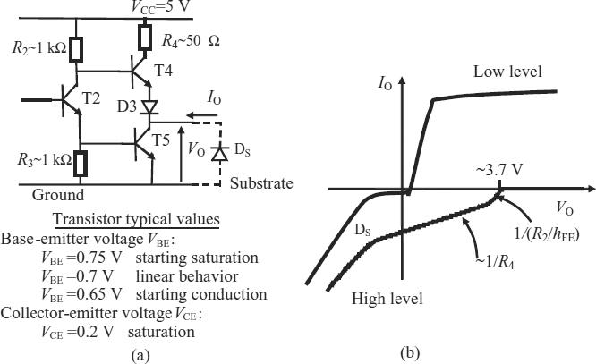
Figure 2.4 Basic TTL device: (a) output stage; (b) output static characteristics at low (L) and high (H) levels
- For values of VO up to about 3 V, transistor T4 is in saturation, the voltage drop between the base and emitter is VBE4 = 0.75 V, and the voltage drop between the collector and emitter is VCE4 = 0.2 V. The voltage in diode D3 is VD3 = 0.75 V. The base current of transistor T4 is IB4 = (3.5 − VO)/R2, and the collector current is IC4 = (4.05 − VO)/R4. This means that
 , and therefore IC4 ≈ IE4 = −IO. The output characteristic is then represented by the line −IO = (4.05 − VO)/R4, and hence ROH = R4 = 50 Ω.
 - When VO approaches 3.7 V, it yields ROH = R2/(hFE + 1), where, in general, hFE = IC/IB is the gain of a transistor, and the current sourced by the emitter is IE = IB + IC. This new value of output resistance is due to the fact that transistor T4 is in the active region, its base current is IB4 = −IO/(hFE + 1), and with the adopted current convention IE4 = −IO. Starting from the supply VCC = 5 V, and taking into account the voltage drop across R2, and the voltages 0.65 V across the base–emitter junction of T4 and 0.65 V across diode D3, this yields VO = 3.7 + R2IO/(hFE + 1). Thus, the output has a Thévenin representation, which consists of a voltage of 3.7 V in series with an output impedance R2/(hFE + 1). With R2 = 1 kΩ and hFE + 1 = 50, it yields VO = 3.7 + 20IO, so that in this case ROH =20 Ω.
- For IO = 0 there is no voltage drop across R4, nor any voltage drop across the base–emitter junction of T4 or diode D3, and, in principle, VO should become equal to VCC = 5 V. Hence, ROH has a very high value.
At low logic output level, T4 is cut off while T2 and T5 are on. The output looks directly across transistor T5, which now sinks a current IO. The volt–ampere characteristic at the output terminals is now precisely the common emitter–collector characteristic of the transistor corresponding to the base current IB5 of transistor T5. Therefore, at low logic output level for VO > 0, two ROL output resistance values can be distinguished:
- when T5 is out of the saturation region, ROL is low (a few ohm) and the voltage drop VO across the transistor has a low value and increases very slowly with large change in current IO;
- when T5 is in saturation, IO and ROL are high, which means that the voltage drop VO across the saturated transistor increases rapidly with small change in current.
For VO < 0, the output characteristic is determined by the substrate diode DS.
A number of types of TTL gate are available, differing principally in the compromise made between speed and power dissipation. Thus, the basic gate is considered a medium-speed gate. A typical high-speed TTL gate is shown in Figure 2.3b. The differences with a basic gate are that another transistor T3 is introduced and diode D3 is not present. The function of D3, included in basic TTL to ensure that T4 will be cut off when T2 and T5 are saturated, is made by the voltage drop across the base–emitter junction of T3. The important characteristic of the improved gate is that, when T3 and T4 are conducting, the gate output resistance is substantially lower than in the basic TTL circuit. Repeating the calculation made for basic TTL, the output resistance is ![]() when the transistor resistance is neglected. This lowered output impedance and the use of Schottky junction technology increase the speed of operation at the gate. Any capacitance shunting the gate output will be able to charge more rapidly. It is interesting to note that, in this configuration, T4 can never saturate.
when the transistor resistance is neglected. This lowered output impedance and the use of Schottky junction technology increase the speed of operation at the gate. Any capacitance shunting the gate output will be able to charge more rapidly. It is interesting to note that, in this configuration, T4 can never saturate.
The basic input static characteristic of a TTL is shown in Figure 2.5. When VI = 0, T2 is cut off and the collector current of transistor T1 is IC1 = 0. In this case, T1 can be roughly represented as a diode. Assuming a 0.75 V junction voltage and R1 = 4 kΩ, it yields II = (5 − 0.75)/4000 = 1.06 mA.
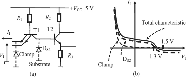
Figure 2.5 Basic TTL device: (a) input circuitry; (b) input static characteristic (not to scale)
As VI increases, the II–VI plot departs from the straight line as T2 begins to turn on. When II = 0, all the current through the 4 kΩ resistor flows into the collector of T1 and into the base of T2. At this point, both T2 and T5 will be in saturation, and the voltage VB2 will be about 1.5 V. The characteristic will begin to depart from the straight line at about 1.3 V.
2.1.3 Complementary Metal Oxide Semiconductor (CMOS) Devices
Complementary Metal Oxide Semiconductor (CMOS) field-effect transistors differ from bipolar both in structure and operation [1]. The primary advantages of the CMOS are its low power dissipation and small physical geometry. Advances in design and fabrication have brought CMOS devices into the same speed and output drive capability as TTL. Again, enhancements have resulted in the evolvement of additional classifications: MG (Metal-Gate CMOS), HC (High-speed silicon-gate CMOS) [17], and FACT (Advanced CMOS) [8].
The most recent evolution in CMOS logic has been in reducing supply voltage without sacrificing performance. The new LCX family is one outgrowth of this trend. This family results from the joint efforts of a triumvirate of companies including Motorola, National, and Toshiba. Although each company has done its own design and fabrication, they have mutually agreed to provide identical performance specifications. In addition to the 3 V operating voltage, LCX inputs and outputs are tolerant of interfacing with 5 V devices. The CMOS inverter is shown in Figure 2.6a. The drains of p-channel and n-channel transistors are joined, and a supply voltage VCC is applied from source to source. The output is taken at the common drain. The input VI swings nominally through the range of VCC that is positive. Because of the complete symmetry of the circuit, the two transistors are chosen to be reasonably alike. A typical I/O static characteristic is shown in Figure 2.6b [1].
When VI = VCC and VO is forced to move from VCC to 0 V, the n-type MOSFET is on, and the p-type MOSFET is off. The output static point moves from the saturation region, where the output impedance ROL is very high, to the triode region, where ROL is low. In the triode region it is found that for an n-channel device
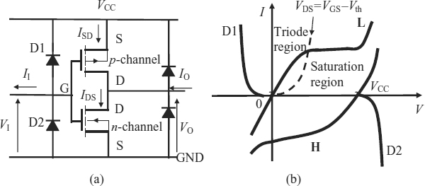
Figure 2.6 CMOS gate: (a) input and output stage; (b) output static characteristics at low (L) and high (H) levels and input characteristic
while in the saturation region
where Vth is the threshold voltage, k = χεw/(2tl) is a constant, χ is the mobility of carriers in the channel (electrons in n-channel devices), ε is the dielectric constant of oxide under the gate, t is the thickness of oxide under the gate, w is the channel width, and l is the channel length.
The impedance in the saturation region is very high; thus, operation in this region should be avoided when driving transmission lines, and matched impedance is required. If the buffer is designed for operation primarily within the triode region, the impedance will vary much less and the output impedance can be considered almost linear and equal to a few ohms.
When VI = 0 and VO is forced to move from 0 to VCC, the n-type MOSFET is off, and the p-type MOSFET is on. The output static point moves from the saturation region, where the output impedance ROH is very high, to the triode region, where ROH is low. In a p-channel transistor, operating in the triode region the equation for device current is more conveniently written in the form
and when operating in the saturation region as
Input diodes D1 and D2 are for protection and determine the input characteristic. Output diodes determine the output characteristic when VO < 0 and VO > VCC.
In the triode area, the equivalent output Thévenin circuit is a voltage source Eout with a swing between 0 and VCC and Rout of a few ohms.
2.1.4 Emitter-Coupled Logic (ECL) Devices
Emitter-Coupled Logic (ECL) derives its name from the differential-amplifier configuration in which one side of the diff-amp consists of multiple-input bipolar transistors with their emitters tied together [1]. An input bias on the opposite side of the diff-amp causes the amplifier to operate continuously in the active mode. Consequently, ECL consumes a relatively substantial amount of power in both states (one or zero), but also results in the fastest switching speeds of all logic families. An inherent benefit of ECL is the narrow switching level swing between devices (approximately 800 mV), which helps to reduce noise generation.
There have also been many evolutionary advancements in ECL: 100K (1975), 10KH (1981), and ECLinPS™ (1987) [6, 15]. Of most recent vintage is the ECLinPS Lite™ family of single-function devices. By focusing on simplicity, this family achieves very high performance while reducing the package size.
The basic circuit configuration employed in the logic ECL with positive power supply (PECL) is shown in Figure 2.7, where the difference amplifier is used to avoid saturation region operation of the transistors [1], giving rise to a high-speed digital device. It is possible to establish a transistor in its active region, with stability, by introducing negative feedback through the simple expedient of using a large emitter resistor. In the present application as a logic gate, the base of transistor T2 is held at a fixed reference voltage VR while an input voltage VI is applied to the base of transistor T1. The bias voltage VR is set at the midpoint of the signal logic swing. When VI is sufficiently lower than VR, T1 will be cut off and current will flow through T2. Voltage VR, the resistance at the collector, and the circuit at the emitter of T2 are selected to ensure that T2 operates in its active region and is not saturated. The emitter current IE, corresponding to input level ‘0’, is IE = (VR − VBE)/RE = 4 mA, with VR = 3.65 V, VBE = 0.8 V, and RE = 713 Ω. The voltage drop across the collector resistance RC2 = 245 Ω of T2 may be calculated as VRC2 = (IE − IB2)RC2 ≈ IERC2 = 0.004 × 245 = 0.98 V. Assuming a voltage VBE = 0.8 V of the emitter follower transistor T3 in its active region as the loading effect of VT and RT, at OR output, it yields VOL = 5 − (0.98 + 0.8) = 3.2 V. This current–voltage point is indicated in Figure 2.7b by QL.
When VI rises to VR, the current in the two transistors will be nominally equal. Finally, as VI continues to increase, the emitter voltage VE on resistance RE increases, as VE = VI − VBE1, with VBE1 approximately constant, and eventually T2 will cut off. We now have T1 operating in its active region. In this case the voltage at OR output is VOH = 5 − (0.8 + 0.1) = 4.1 V. This current–voltage point is indicated in Figure 2.7b by QH, assuming that T2 is near the cut-off region with a collector current that causes a voltage drop on the collector resistance of 0.1 V.

Figure 2.7 ECL device: (a) output stage; (b) output static characteristics at low (L) and high (H) states
The two outputs, OR and NOR, have complementary voltages that can be used for differential mode transmission. Thus, the mechanism of operation consists in switching a nominally fixed emitter current from one transistor to the other with very little change in emitter current. Outputs are taken at the collectors through emitter followers, which drops the collector voltage level one base-emitter drop. The emitter follower provides buffering and low impedance at the output terminals.
Considering the positive direction of IO when the current is sourced by the output for convenience of representation, the I–V output static characteristic is shown in Figure 2.7.
Taking into account that the base current on the output transistor is IB3 ≈ IO/hFE, where hFE is the transistor gain, and that the current on the collector of transistor T2 is about IE, the point QL is the interception between the line VCC − (IE + IO/hFE) RC2 − VBE = VO (or, adopting the convention of Figure 2.7b, IO = −hFE/RC2VO + hFE/RC2(VCC − IERC2 − VBE)) and the line IO = VO/RT − VT. With hFE = 50, the output resistance of the ECL gate is Rout = RC2/hFE ≅ 5 Ω. Note that VO =3.2 V for IO = 0. The point QH of Figure 2.7b is calculated with the IERC2 term missing because T2 is cut off. In this case Rout is again 5 Ω and VO = 4.2 V for IO = 0. The output equivalent circuit of an ECL is therefore a voltage generator with a swing from 3.2 to 4.2 V and a series resistance of 5 Ω. This means that ECL is suitable for a driving transmission line with low Z0, e.g. 50 Ω, and in matching condition when RT = 50 Ω.
2.1.5 Low-Voltage Differential Signal (LVDS) Devices
Low-Voltage Differential Signal (LVDS) is defined in the TIA/EIA-644 standard and can be designed using CMOS processes [7, 13]. It is a low-voltage, low-power, differential technology used primarily for point-to-point and multidrop cable driving applications. The standard was developed under the Data Transmission Interface committee TR30.2. It specifies a maximum data rate of 655 Mbps, although some of today's applications are pushing well above this specification for a serial data stream.
Compared with other differential cable driving standards like RS422 and RS485, LVDS has the lowest differential voltage swing of 700 mV, and a typical offset voltage of 1.25 V above ground. The output stage of an LVDS device is shown in Figure 2.8.
According to the direction of the output current IO, the voltage VO referred to ground (see output Q+) can have values of 0.9–1.1 or 1.3–1.5 V considering the low and high level outputs of a CMOS gate. LVDS features a low swing differential constant current source configuration, which supports fast switching speeds and low power consumption. LVDS is a valid alternative to PECL devices for differential signal transmission. The characteristic of this technology used for differential signaling will be investigated in more detail in Section 12.1.
2.1.6 Logic Devices Powered and the Logic Level
The average power dissipation Pavg of a digital device that must charge and then discharge its capacitive load C through a series resistance R every cycle with period T and swing voltage V can be calculated considering that the voltage across the capacitor during the charging time is V(t) = V(1 − e−t/RC). The instantaneous power drawn from the supply is

Figure 2.8 LVDS device output stage
Integrating the power (2.5) over a half cycle and dividing by the full period yields

Therefore, for a data line with transitions on the rising or falling edge of the clock, the average power dissipation is ![]() .
.
With the square dependence on voltage, the reduction in voltage is the most effective way of reducing power dissipation. The trend in developing new logic devices is therefore to lower power supply and increase speed. Logic families with a power supply at 5 V include TTL, ACMOS, and PECL, and those at 3.3 V include LVT, LVC, LCX, GTL, and LVDS. The values of voltages VOHmin, VIHmin, VOLmax, and VILmax for several logic families are shown in Figure 2.9, so that their immunity noise can be compared. These values are very important, as a successful communication requires that driver and receiver agree on what voltage levels constitute logic low and logic high. For voltage-mode signaling such as TTL, the driver directly sets the output voltage.
For current-mode signaling such as ECL in differential mode and LVDS, the driver sets the current level, and the voltage drop across a termination resistor at the receiver is detected. In either case, it is sufficient to discuss signaling in terms of the voltages set by the driver and the voltages detected by the receiver.
2.2 Dynamic Characteristics: Gate Delay and Rise and Fall Times
The main dynamic parameters of a logic gate are:
- gate or propagation delay time TGD;
- rise time tr and fall time tf.

Figure 2.9 Logic voltage levels for some logic families
The gate delay time TGD is defined in Figure 2.10. It is the delay between the input and output voltages of the device taken at the threshold voltage level Vth where the device changes state. The threshold voltage Vth depends on the logic device used. For example, with the TTL family, Vth = 1.5 V. The gate delay time TGD for high-to-low (TGD-HL) and low-to-high (TGD-LH) logic state transitions is very important because it affects the jitter and skew defined in Chapter 1. Rise time tr and fall time tf parameters are defined in Figure 2.11. The rise time tr is the time required for VO to go from 10 to 90 % of the voltage swing Vsw. The fall time tf is the time required to go from 90 to 10 % of Vsw. The times tr and tf could be different for the same device, for instance, FAST has tr = 3 ns and tf =1 ns; on the other hand, FACT has tr = tf = 2 ns.
These parameters are very important when a system designer has to decide whether an interconnect must be considered as a ‘short line’ or as a ‘long line’. In Chapter 5 it will be shown that, if tr/tf < 2tpdl, where tpd is the per-unit-length propagation delay time of the interconnect between two gates and l is the length of this link, the line must be considered as ‘long line’ and simulated as a transmission line instead of a lumped line capacitance.

Figure 2.10 Delay parameters: (a) final stage of a CMOS gate; (b) gate delay parameters

Figure 2.11 Definition of rise tr and fall tf times
Dynamic parameters tr and tf depend mainly on the number of simultaneously switching gates, loads, decoupling capacitors, package, and power distribution. Consider that measuring tr and tf with only one gate switching without load leads to an overdesign. It is important to find out typical cases or an average between two extreme cases.
Typical dynamic parameters of some traditional logic families are summarized in Table 2.1. The dynamic performance of the up-to-date devices used for very high-speed systems such as LVDS and PECL will be discussed in Chapter 12.
2.3 Driver and Receiver Modeling
The problem of how to model the driver and the receivers of an interconnect correctly is a very important topic in signal and power integrity predictions. There are simple models suitable for predicting reflections and crosstalk, and other more complex models for predicting ΔI-noise. The purpose of this section is to help the reader in choosing the most appropriate model for the problem of interest.
2.3.1 Types of Driver Model
There are three general types of driver model that can be used in the simulation of digital systems:
- Linear models.
- Behavioral models.
- Full transistor models.
In many practical cases of interconnects, the first two types of model are suitable for reflection and crosstalk predictions. These models are similar because they adopt a Thévenin equivalent circuit to simulate the output stage. This circuit is constructed from curves describing the I/O static current–voltage characteristic, and considering the dynamic performance during the switching of the output gate. Numerous examples of application of these models are provided in Chapter 5 and Chapter 6. These types of model are the basis of the IBIS models provided by the manufacturers of devices in a standard format. The IBIS models are introduced and described in Section 2.4. A description of up-to-date behavioral models that consider several phenomena within digital devices, such as non-linear behavior and switching noise, can be found elsewhere [19–22]. Models of the third type are used for modeling the input, intermediate, and output stages of an IC device at the transistor and diode level. They may be necessary when crosstalk and simultaneous switching noise in IC devices must be simulated (see the example given in Section 8.4).
Table 2.1 Dynamic parameters of some logic families

2.3.2 Driver Switching Currents Path
Drivers fall into two basic categories: push-pull and current steering. The push-pull drivers use transistors to connect the output to either of two voltage levels to indicate the logic state (TTL, CMOS). The current-steering drivers use two different levels of current to indicate logic state, where the current is converted to voltage at a termination resistor to enable detection (differential-mode ECL, LVDS).
The main disadvantage of a push-pull driver is the extra current required from the power supply by the simultaneous conduction of the two transistors when they are switching. This current is indicated as crowbar or shoot-through current in Figure 2.12. This does not happen with current-steering drivers. Other switching currents are required to charge and discharge line and load capacitors, as illustrated in Figure 2.12.
If the effects of crowbar current can be neglected, as occurring in the presence of a quasi-ideal bypass capacitor between power supply leads and ground (associated lead inductance very low), the transmitted and received waveforms on the signal line can be simulated with the point-to-point structure shown in Figure 2.12c. In fact, ground and power supply conductors are at the same potential in the high-frequency range, and the return signal current can refer to both.
Any non-linear circuit can be made linear and represented by a Thévenin equivalent circuit. Modeling a driver with equal pull-up and pull-down output impedance consists in assigning the driver’s output voltage swing and slew rate to the Thévenin voltage source, and the driver’s output impedance to the Thévenin equivalent impedance. For example, if the driver is a CMOS that can swing from 0 to 5 V in 2 ns, then the Thévenin source voltage is a linear independent voltage source swinging from 0 to 5 V in 2 ns without load. The Thévenin impedance is a resistance equal to the output impedance of the driver calculated as the average value during the transition. A critical point is the choice of the edge rate in terms of rise and fall times. In fact, these times are different if the gate drives large capacitive loads or long transmission lines.

Figure 2.12 CMOS driver: (a) switching path for output changing from low to high state; (b) switching path for output changing from high to low state; (c) point-to-point interconnect with capacitive load
Logic families suitable for being modeled by a linear circuit are differential-mode ECL and LVDS because they are used with controlled interconnects (a fixed characteristic impedance is required), and a termination is used to match the line. For other logics, a non-linear model is required, especially when terminations are not used
2.3.3 Driver Non-Linear Behavioral Model
The construction of a behavioral model of a non-linear driver by using a Thévenin equivalent circuit is described considering typical CMOS static output characteristics (see Figure 2.13). The first step is to divide the low and high static curves into three segments, as shown in Figure 2.13b: L1, L2, L3 for the low state and H1, H2, H3 for the high state. As each of these segments for both low (L) and high (H) states in the I–V plane are described by the line equation IO = (VO − EO)/RO, they can be simply identified by two parameters EOL or EOH, as the interception of the line with the voltage axis VO, and the line slope 1/ROL or 1/ROH. The voltage VOL or VOH, as the interception of two adjacent segments, characterizes the point of change from one segment to another. For example, VOL2 is the interception of segments L2 and L3, and V0H1 is the interception of segments H1 and H2.
The second step is to assign dynamic values to the Thévenin equivalent circuit parameters, which are the voltage source EO and the resistance RO, considering the switching performance of the type of driver (see Figure 2.13a). For example, with a CMOS buffer that drives an interconnect of typical characteristic impedance in the range 50–150 Ω, the starting point in the I–V characteristic lies on segment L2 before the low-to-high switching (EOL2 in Figure 2.13b), and on line H2 after the rise time tr (EOH2 in Figure 2.13b). In the case of high-to-low switching, the starting point is on segment H2, and after the fall time tf it is on segment L2. In fact, as will be explained in Chapter 5, the values of IO and VO after low-to-high switching can be found as the interception of the line with slope −1/Z0 passing from the static point on segment L2 with segment H2. The values of IO and VO after the high-to-low switching can be found as the interception of the line with slope −1/Z0 passing from the static point on segment H2 with line L2. This means that the equivalent circuit of the driver, in the interval time tr, can be simulated by a voltage source EO that changes from EOL2 to EOH2, and RO that changes from ROL2 to ROH2. In the interval tf, EO changes from EOH2 to EOL2, and RO from ROH2 to ROL2, as shown in Figure 2.13c. Outside this short interval, as happens with high-speed logic, EO and RO are a function of the output voltage VO and have the task of reproducing, according to the value of VO, the segment Li or Hi, where i = 1,…, 3, of the static output characteristic of the driver. All this can be implemented in a SPICE-like circuit simulator by using the ‘if’ operator and tables in the time domain.

Figure 2.13 Behavioral model for CMOS: (a) output equivalent circuit; (b) output static characteristic (solid line) and its segmentation (dashed line); (c) dynamic characteristic
The procedure adopted for CMOS can be repeated for TTL with some differences due to the technology. The static characteristic at the low state is divided into four segments, L1, L2, L3, and L4, and the static characteristic at the high state is divided into three segments, H1, H2, and H3, as shown in Figure 2.14.
As the TTL buffer also drives interconnects with a typical characteristic impedance in the range 50–150 Ω, the starting point in the I–V characteristic lies on segment L3 before the low-to-high switching (EOL3 in Figure 2.14b) and on segment H1 after time tr (EOH1 in Figure 2.14b). In the case of high-to-low switching, the starting point is on segment H3 (EOH3 in Figure 2.14b) and after time tf on segment L3 (EOL3 in Figure 2.14b). In fact, the values of IO and VO after the low-to-high switching can be found as the interception of the line with slope −1/Z0 passing from the static point on segment L3 with segment H1. The values of IO and VO after the high-to-low switching can be found as the interception of the line with slope −1/Z0 passing from the static point in segment H3 with segment L3. This means that the Thévenin equivalent circuit of the driver, in the time interval tr, can be simulated by a voltage source EO that changes from EOL3 to EOH1 and RO that changes from ROL3 to ROH1. In the time interval tf, EO changes from EOH3 to EOL3 and RO from ROH3 to ROL3, as shown in Figure 2.14c. Outside this short interval, as happens with high-speed logic, EO and RO are functions of the output voltage VO and have the task of reproducing, according to the value of VO, the segment Li, where i = 1,…, 4, or Hj, where j = 1,…, 3, of the static output characteristic of the driver.

Figure 2.14 Behavioral model for TTL: (a) output equivalent circuit; (b) output static characteristic (solid line) and its segmentation (dashed line); (c) dynamic characteristic
Examples of the accuracy of these models for calculating reflections and crosstalk will be given in Section 6.4 with TTL and CMOS gates. The package effects within the driver are also taken into account with the addition of resistance, inductance, and capacitance circuit elements.
2.3.4 Receiver Non-Linear Behavioral Modeling
The primary function of the receiver is to detect the logic level of an analog waveform in the presence of noise. To accomplish this task, the receiver offers very high impedance in the interval of the voltage logic swing and the protection of diodes outside this region. The input equivalent circuit of the receiver behavioral model is shown in Figure 2.15, as well as the input static characteristics of TTL and CMOS. In the case of TTL receivers, a diode is used when the input voltage VI < 0 V, and this is fundamental in mitigating reflections. With CMOS receivers there are two diodes, one for VI < 0 V and the other for VI > VCC, where VCC is the power supply value. These two diodes act in mitigating reflection and protect the device from ESD.

Figure 2.15 Behavioral model for TTL and CMOS receivers: (a) input equivalent circuit; (b) input static characteristic
In any case, a receiver can be represented as a circuit element by a voltage-dependent current generator using tables. Also, it is very important to include in the model the input capacitance of the receiver, which is usually some pF. This capacitance has a great effect on signal integrity, especially for lines with distributed loads or loads concentrated at the opposite end of the driver, as will be shown in Chapter 5.
2.4 I/O Buffer Information Specification (IBIS) Models
I/O Buffer Information Specification (IBIS) is a fast and accurate behavioral method of modeling I/O buffers on the basis of I/V curve data derived from measurements or full-circuit simulations. IBIS uses a standard software parsable format to create the behavioral information needed to model analog characteristics of ICs in order to simulate reflections and crosstalk in interconnects of digital devices [23, 24]. IBIS was originally started by Intel, and is presently driven by the IBIS open forum consisting of software vendors, computer manufacturers, semiconductor vendors, and universities. The first version was released in April 1993, focusing on bipolar TTL and CMOS logic components. Other versions were ratified in subsequent years, with many new capabilities that have increased its accuracy and the number of device types that are supported, such as ECL, differential, open-drain I/O devices, and expanded package model definitions to include coupling between pins and other features. The advantages of IBIS are:
- Protection of proprietary information.
- Accurate model of non-linear I/O characteristics, package structure, and devices for ESD protection.
- Signal integrity simulation on system board.
- Models available from semiconductor vendors for free.
- Faster simulation time compared with structural methods.
- Compatibility with all industrial simulation platforms.
- No additional resources required for customer support.
2.4.1 Structure of an IBIS Model
An example of a block diagram for an IBIS behavioral model is shown in Figure 2.16, while the basic elements that must be included for IBIS modeling of an I/O structure are shown in Figure 2.17. The elements of the IBIS model correspond to the keywords in the IBIS format specification. The pull-down element contains the I/V pull-down information, including the typical, minimum, and maximum currents for the given voltages of the pull-down. The pull-up element contains the I/V pull-up information, modeling the characteristics of the buffer when driven high. Note that the voltages in the pull-up and power-clamp tables are VCC relative and are derived from the equation
The IBIS table lists voltages from −VCC to 2VCC. The wide voltage range is provided to improve the accuracy of certain simulators. Many simulators benefit from including these characteristics in the model. For simulators that do not extrapolate unspecified voltages, the ranges given are more than adequate.

Figure 2.16 IBIS behavioral block diagram
The clamp diode characteristics are meant to be modeled in parallel with the driver information as pull-down and pull-up, ensuring that the diode characteristics are present even when the output buffer is in a high-impedance state (off). The currents listed in the table can be large and are provided only to enable simulators to construct the proper diode curve.
The element containing the ramp time for the pull-up and pull-down structures ensures the correct time operation of the model. There is a ‘typ’ column together with ‘min’ and ‘max’ columns. The ‘min’ column represents the longest rise/fall times, and the ‘max’ column represents the shortest times. These values often appear very small because they are intrinsic values for transistors with all packaging and external loads removed. The packaging characteristics are added outside the transistor model. The packaging element in the model includes the inherent capacitance of the silicon portion of the die, Ccomp, and not the package. The package is modeled by the parameters Rpkg, Lpkg, and Cpkg, schematically organized as shown in Figure 2.17. The table supplies the range (minimum-to-maximum) for each parameter.

Figure 2.17 Circuit element of an IBIS model: (a) input model; (b) output model
With the IBIS data, signal integrity designers can model the device characteristics for both fast and slow switching edges. The slow model can be used to determine the propagation time. The fast model can be used to simulate overshoot, undershoot, and crosstalk. A slow model can be created by combining the minimum currents with the maximum ramp time and maximum package element values. A fast model can be created with the largest currents, the fastest ramp, and the minimum package element values. The minimum and maximum data include both temperature and process variations. Voltage variation is normally adjustable within simulation tools, or can be approximated by shifting the I/V data by the desired voltage tolerance. The input model includes I/V curves for diodes only.
2.4.2 IBIS Models and Spice
To use IBIS models in SPICE, an IBIS-to-SPICE translator is required, as some simulators cannot use the IBIS file directly. It must be translated into a usable model language. Typically, the conversion leads to a SPICE-compatible syntax. On the other hand, codes for professional users, such as HSPICE and Eldo, handle IBIS models directly.
An example of using an IBIS model with SPICE will be provided here by using Micro-Cap version 9, which has the required translator [25]. The input file should have an IBIS extension (.ibs), and a .lib extension is usually assigned to the output file to indicate its use as a library file, although it also contains SPICE code for plotting the translated buffer models.
In the example considered the component 74AC244SC (file name ac244sc 450.ibs.) is adopted. This is not an up-to-date device – it refers to version 2.1. However, our intention is to give basic information concerning a typical IBIS format to help understand the more recent versions and how to use the information provided for signal integrity simulations by SPICE. Other files regarding the components of interest can be downloaded from the web as ‘xxx.ibs’, provided by the component manufacturers. The static I/V and dynamic output characteristics extracted by the IBIS file, using the ASCII data contained in the IBIS file, are shown in Figure 2.18. The input model uses the same clamp to power and ground characteristics as the output model. Voltage and current sign conventions are those used in Section 2.3: positive current sunk by the driver and voltages referred to ground.
The simulated waveforms shown in Figure 2.19 concern the case of the driver and receiver connected by a transmission line of characteristic impedance Z0 = 50 Ω and delay time TD = 3 ns. Observe that maximum values produce overshoot and undershoot, while minimum values produce extra delay.
When a user has a low-cost circuit simulator that does not have the feature to translate automatically the IBIS format to SPICE, the information contained in the IBIS file can be used to obtain similar curves and waveforms to those in Figure 2.19. Then the component can be modeled as outlined in Section 2.3.
To give an idea of the type of accuracy achievable with these types of model, many examples of signal integrity investigations using models similar to IBIS obtained by measurement of the I/O characteristics will be provided in Chapter 6. Simple behavioral I/O models to implement into SPICE will also be described for the case where the user does not have a IBIS-to-SPICE translator available.

Figure 2.18 Static and dynamic characteristics of the device 74CA244 buffer as obtained by its IBIS model: (a) pull-up and pull-down I/V output; (b) rise and fall times; (c) clamp ground; (d) clamp power. Typical (solid line), minimum (dotted-dashed line), and maximum (dashed line)
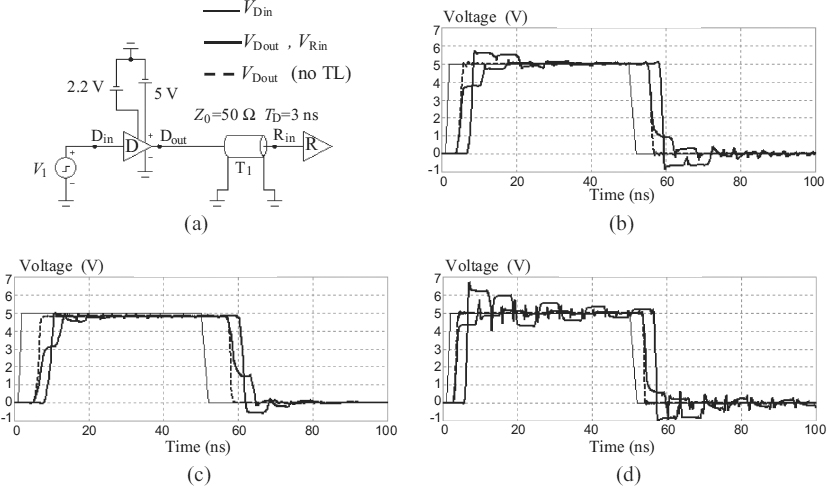
Figure 2.19 Example of signal integrity investigation by using 74AC244 IBIS models for driver (D) and receiver (R) translated into SPICE: (a) interconnect structure; (b) simulated waveforms with typical values; (c) with minimum values; (d) with maximum values
References
[1] Taub, H. and Schilling, D., ‘Digital Integrated Electronics’, McGraw-Hill Education, New York, NY, 1977.
[2] Blood, W., ‘MECL System Design Handbook’, 4th edition, Motorola Semiconductor Products, Inc., Phoenix, AZ, 1983.
[3] Morris, R.L. and Miller, J.R., ‘Designing with TTL Integrated Circuits’, McGraw-Hill, New York, NY, 1971.
[4] ‘LVT Family Characteristics’, AN-SCEA002A, Texas Instruments, 1998. Available online: www.ti.com.
[5] ‘LVT (Low Voltage Technology) and ALVT (Advanced LVT)’, AN-243, Philips Semiconductors, 1998. Available online: www.nxp.com.
[6] ‘Designing with PECL (ECL at +5 V)’, AN-1406, Motorola Semiconductor, Rev. 2, August 2001. Available online: www.freescale.com.
[7] ‘LVDS Description and Family Characteristics’, MS500530, Fairchild Semiconductor, 2000. Available online: www.fairchildsemi.com.
[8] ‘FACT™ Descriptions and Family Characteristics’, MS010158, Fairchild Semiconductor, 2000. Available online: www.fairchildsemi.com.
[9] ‘ABT: Description and Family Characteristics’, MS011558, Fairchild Semiconductor, 1999. Available online: www.fairchildsemi.com.
[10] ‘LVT Family Introduction’, MS000227, Fairchild Semiconductor, 1999. Available online: www.fairchildsemi.com.
[11] ‘LVX Family Introduction’, MS000217, Fairchild Semiconductor, 1999. Available online: www.fairchildsemi.com.
[12] ‘AC/DC Family Characteristic Comparison’, MS500120, Fairchild Semiconductor, 1999. Available online: www.fairchildsemi.com.
[13] ‘LVDS Fundamentals’, AN-5017, Fairchild Semiconductor, 2000. Available online: www.fairchildsemi.com.
[14] ‘GTLP: an Interface Technology for Bus and Backplane Applications’, AN-1065, Fairchild Semiconductor, 2001. Available online: www.fairchildsemi.com.
[15] ‘ECL Backplane Design’, AN-768, Fairchild Semiconductor, 2000. Available online: www.fairchildsemi.com.
[16] ‘Transmission-line Effects Influence High-Speed CMOS’, AN-393, Fairchild Semiconductor, 1985. Available online: www.fairchildsemi.com.
[17] ‘Comparison of MM74HC to 74LS, 74S and 74ALS Logic’, AN-319, Fairchild Semiconductor, 1983. Available online: www.fairchildsemi.com.
[18] ‘FAST/FASTr Design Considerations’, AN-661, Fairchild Semiconductor, 1990. Available online: www.fairchildsemi.com.
[19] Mutnury, B., Swaminthan, M., Cases, M., Pham, N., de Araujo, D., and Matoglu, E., ‘Macromodeling of Nonlinear Transistor-level Receiver Circuits’, IEEE Trans. on Advanced Packaging, 29(1), February 2006, 55–66.
[20] Mutnury, B., Swaminthan, M., Cases, M., and Libous, J., ‘Macromodeling of Nonlinear Digital I/O Drivers’, IEEE Trans. on Advanced Packaging, 29(1), February 2006 102–113.
[21] Stievano, I., Maio, I., Canavero, F., and Siviero, C., ‘Reliable eye-diagram analysis of data links via device macromodels’. IEEE Trans. on Advanced Packaging, 29(1), February 2006, 31–38.
[22] Stievano, I., Maio, I., Canavero, F., and Siviero, C., ‘Parametric macromodels of differential drivers and receivers’, IEEE Trans. on Advanced Packaging, 28(2), May 2005, 189–196.
[23] ‘IBIS (I/O Buffer Information Specification), Version 4.1’, Ratified 30 January 2004.
[24] IEC 62014-1: ‘Electronic Design Automation Libraries – Input/Output Buffer Information Specification (IBIS version 3.2)’.
[25] www.spectrum-software.com.
Signal Integrity and Radiated Emission of High-Speed Digital Systems Spartaco Caniggia and Francescaromana Maradei
© 2008 John Wiley & Sons, Ltd