
12
Differential Signaling and Discontinuity Modeling in PCBs
The differential transmission technique is the best way to ensure high-speed data functionality and immunity to the system for signaling at PCB and cable level. The advantages of using differential-mode (DM) transmission versus single-ended transmission are presented in this last chapter. Techniques for implementing differential signal transmission in a system are outlined, referring to the Advanced Telecommunications Computing Architecture (ATCA) standard. This standard is adopted by many companies involved in the development of very high-speed systems for telecommunications. LVDS is one of the most popular devices for differential-mode transmission. For this reason, LVDS characteristics and performances are shown in comparison with other families. The results obtained in terms of signal integrity (SI) and induced noise from an experimental set-up that uses test boards with LVDS drivers and receivers are presented and discussed. It is also shown that, by adding pulse transformers at driver and receiver locations, the immunity of the LVDS to a common-mode (CM) noise voltage can rise over 40 V instead of the specified ±1 V. Crosstalk in differential signaling with overhead and coplanar traces is investigated by SPICE simulations. Moreover, some design rules are provided for trace routing. An example of the realization of a motherboard according to the ATCA standard is presented, and its performance in terms of crosstalk and data rate transmission are verified by measurements.
The chapter ends by considering how to model discontinuities occurring in PCB interconnects and IC packages in order to extract equivalent circuit models to be used in SPICE simulations. Equivalent circuits of bends, vias, connectors and ground slots are presented. Some investigations and model validations are performed by 3D numerical codes. It is shown that differential transmission is appropriate when a signal must cross a gap in a ground plane without significant deterioration in the signal integrity and EMI performance. Finally, package types of connection for ICs are presented and discussed.
12.1 Differential Signal Transmission
In the past, differential signal transmission was mainly used to transmit signals between PCB racks or apparatus by using twisted-pair cables as an economical solution capable of improving the immunity of the interconnects. Differential transmissions were implemented in PCBs by ECL devices for EMI and speed reasons. However, the price to pay was high power dissipation due to the nature of ECL devices operating with the transistor in the linear region, thereby sinking a large amount of current from the power supply in static conditions as well. With the improvements in CMOS technology in terms of transistor size and speed, and with the possibility of powering the devices with lower voltages, differential transmission makes it possible to operate over 1 GHz with appropriate signal integrity and EMI performance.
The basic concepts of a differential signaling transmission are treated in several textbooks [1–5] and Application Notes (ANs) prepared by the companies in charge of the design, development and selling of devices [6–14]. This chapter begins by considering the advantages offered by the differential technique, and some experimental and simulated results will be discussed to set design rules for enhancing receiver immunity, trace routing and line terminations in a PCB.
12.1.1 Single-Ended Versus Differential Signal Transmission
A differential signal provides maximum noise immunity. This is because any noise coupled with a pair of closed–parallel conductors generally appears equally on both conductors, so that this noise has the form of a common-mode noise. Whereas the receiver responds only to a voltage difference across the lines, in a twisted-pair cable the crosstalk noise can be ignored in many practical cases, as it is picked up equally by each of the two lines. This holds true up to the common-mode noise rejection limit of the receiver [5]. In the following, this feature will be discussed in more detail.
Three kinds of signal transmission are shown in Figure 12.1: single-ended, unbalanced and balanced (differential). In this figure, the following notation is adopted:
- Vs is the signal at the driver (i.e. source) output.
- Vr is the signal at the receiver input affected by noise.
- Vi is an interfering disturbance on the signal conductor owing to crosstalk or radiated fields.
- Vn is a noise on the ground conductor owing to interfering currents such as the return current of other signals, electrostatic discharge, surge, etc.
- gnd is the reference voltage point for the system.
- Δ before a symbol of a common-mode voltage means the fraction of that voltage that converts to a differential-mode voltage owing to asymmetries in the interconnect structure.
Single-ended Transmission
The structure consists of two conductors: one is used for transporting signal current and the other is used as the return path, as shown in Figure 12.1a. The ground conductor could be in common with other signal conductors. The voltage Vr is the algebraic sum of the signal voltage Vs, with delay when the line is matched, and the noise voltages Vi and Vn caused by external interferences. This means that the total disturbance (±Vi ±Vn) affects the receiver directly. For this reason, the immunity is poor.

Figure 12.1 Signaling in the presence of external noise: (a) single-ended; (b) unbalanced; (c) balanced (differential transmission)
Unbalanced Transmission
The structure consists of three conductors: one conductor is used for transporting signal current, a second conductor, symmetric to the first, is used as the return path, and a third is used as reference ground where the ground pins of the driver and receiver are connected. The driver is a single-ended device and the receiver is differential, as shown in Figure 12.1b. This means that the receiver inputs recognize the voltage difference across the two ends of the signal conductors. The differential signal voltage Vr at the receiver is the algebraic sum of the signal voltage Vs and the voltages ΔVi and ΔVn of the disturbances Vi and Vn respectively. These disturbances come from the conversion of common mode to differential mode and are mainly caused by the unbalanced structure of the driver. This improves the immunity of the interconnect with respect to the single-ended solution, but it is not suitable for high-speed interconnects.
Balanced Transmission
The structure is similar to the previous one, the difference being that the driver is also differential. The driver has two outputs switching with opposite polarity and equal output impedance in order to excite a differential mode according to the definition given in Section 6.2. In this case, if the structure is perfectly symmetric, Vr should be equal to Vs with the delay of the interconnect. This does not occur in practice because of the slight non-symmetry of the driver, conductors, and receiver with respect to the reference ground. Common-mode to differential-mode conversion always exists, but the fractions ΔVi and ΔVn, which sum algebraically to Vs, are very small.
An ideal receiver should be able to reject common-mode disturbances of any values. In practice this is not the case, and a receiver is characterized by a parameter, the common-mode rejection, that defines the ability of the receiver to work properly up to a defined amount of common-mode noise. This parameter varies from a few to several volts, depending on the speed of the device. For example, a receiver of series RS422 has immunity to common-mode disturbance of ±7 V. LVDS devices are faster but offer less immunity (±1 V).
A differential signal is transmitted on a dual-signal path, and the two signals are driven as a complementary pair, with one signal being the logic inverse of the other. In this case, the signal quality can be measured by the technique described in reference [15].
As shown in Figure 12.1c, the differential signal involves a differential transmitter, a differential interconnect, and a differential receiver. The ground potential difference between the transmitter and the receiver is modeled as a noise voltage source and can have both DC and AC components. High-speed data links use differential signaling at much higher frequencies where noise problems tend to be more severe, even for relatively short connections.
The advantages of differential signaling in high-speed data transmission include the following:
- higher common-mode noise rejection;
- increased noise immunity;
- reduced crosstalk;
- reduced ground noise;
- reduced EMI;
- a better eye diagram than a single-ended signal, with a non-solid reference plane of the PCB.
Differential signaling is able to reject common-mode noise from ground potential variations between transmitter and receiver, and other injected noises that are common to both signal paths. The transmitted differential signal is processed at the receiver as the voltage difference between the two lines. By taking the difference between the two complementary signals, the differential receiver also produces twice the signal swing of a single-ended signal for improved noise immunity.
The balanced nature of differential signals in general leads also to a more constant switching current than that of single-ended circuits. The signal currents in differential drivers tend to be steered between the two outputs as the signal polarity switches, which results in a more constant load current compared with the load current spikes commonly seen with single-ended drivers. Reduced load current transients should also result in a reduction in that portion of ground noise that is caused by current spikes passing through the ground lead inductance. The improved noise immunity and high sensitivity of differential receivers also allows the use of reduced logic swings with differential signaling. This smaller signal swing and the balanced field distribution associated with differential signaling generate less EMI.
The drawbacks of using differential signaling are:
- the increased layout complexity;
- the need for balanced signals and interconnects.
The common use of point-to-point connections rather than a shared bus structure results in separate paths for transmitted and received signals, which effectively doubles the number of signal pairs required in a high-speed serial link. Consider also that imbalance in differential signaling paths leads to the generation of common-mode currents and reduced common-mode rejection at the receiver. An experimental investigation regarding the generation of common-mode current by differential drivers such as RS422, LVDS, and PECL and its effects in producing radiated fields is reported in Section 9.7, considering the EMI performance of UTP and SFTP cables and their connectors.
12.1.2 Differential Interconnect with Traces in PCBs and the ATCA Standard
When considering the transmission characteristics for a differential signaling interconnect between two boards, the complete end-to-end path of the connection must be taken into account. End-to-end signal skew and propagation delay time must be properly understood to ensure interoperability between boards and backplanes. These requirements are fundamental to the Advanced Telecommunications Computing Architecture (ATCA) standard proposed by a consortium of companies for the development of very high-speed systems for telecommunications [16]. ATCA is the largest specification effort in the history of the PCI Industrial Computer Manufacturers' Group (PICMG), with more than 100 companies participating. The official specification designation is PICMG 3.x. Here, AdvancedTCA™ is targeted to requirements for the next generation of ‘carrier-grade’ communications equipment. This series of specifications incorporates the latest trends in high-speed interconnect technologies, next-generation processors, and improved Reliability, Availability and Serviceability (RAS). In this section, the main characteristics and performance will be highlighted.
A typical point-to-point differential signal connection is defined by three main components, as shown in Figure 12.2: the trace routed across the backplane, pair connectors at each end, and the trace routing on the board between the connector and the transmitter/receiver.
Equalization is a high-pass filtering technique applied to the signal interconnect to compensate for the increase in interconnect attenuation with frequency. The simplest implementation of equalization is to use an AC-coupling capacitor Ce in series with the pair of conductors in order to form, with the termination resistor Rt, a high-pass filter as shown in Figure 12.2. As the termination resistor is set by the differential characteristic impedance of the interconnect, the value of the AC-coupling capacitor should be selected to match the desired equalization response [15].
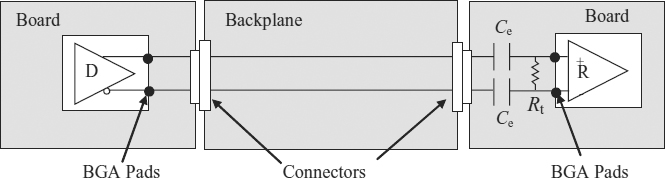
Figure 12.2 Typical point-to-point differential connection with Ball Grid Arrays (BGAs)

Figure 12.3 Suggested differential interconnect structure in a PCB. All dimensions are in mm
If vias must be used in the signal routing path, via design should try to minimize the associated inductance and capacitance, and these parasitic parameters should be matched in both traces of a differential pair. Other examples of routing parasitic parameters are the parasitic input capacitances present at the input pin of a serial data receiver, and package parasitic parameters present in a circuit-board-mounted serial data connector.
An electrical cable for the transmission of high-speed serial data is often shielded, and the differential signal path is typically implemented with twisted pairs. Twisted pairs are used for differential signal impedance control and to minimize crosstalk between the transmit and receive signaling pairs.
High-speed serial data interconnects on circuit boards also require the use of a differential signal routing technique. Differential signal interconnects are routed as coupled transmission lines. Generally, there is close spacing between circuit board traces and board ground planes, so that the degree of coupling between differential lines on a circuit board is much less than that for twisted pairs, particularly for edge-coupled lines. This limited coupling between circuit differential pairs means that it is not uncommon to see differential pairs routed separately on circuit boards as two uncoupled transmission lines.
Coupled lines can be routed in several different ways, depending on the layout requirements. Edge-coupled lines, where the traces are routed side by side on the same circuit board layer, are commonly placed on the outer layers as microstriplines, although they can be embedded as inner-layer striplines. Broadside-coupled lines should generally be routed only on inner layers as striplines in order to provide a symmetrical structure.
An example of an edge-coupled backplane single stripline with FR4 dielectric, taken from reference [16], is shown in Figure 12.3. The coupling between traces within a pair in this structure is significant. Therefore, maintaining the typical 0.254 mm spacing throughout the length of the pair is very important to keep the 100 Ω differential impedance constant. The distance between any two pairs must be no smaller than 0.889 mm edge to edge, as shown in Figure 12.3. This limits crosstalk to lower than 0.2 % (near-end coupling coefficient, NEXT), as will be shown by simulations in the next section devoted to LVDS devices. The 0.889 mm spacing derives from the relative dielectric constant of the FR4 material, as outlined in Chapter 6. For high-density routing, simulations are required.
The differential characteristic impedance Z0DM of a pair of traces, like that shown in Figure 12.3, can be calculated by the approximate formula [8]


Figure 12.4 Output level comparison of four differential family devices
The parameters b, w, and s are shown in Figure 12.3. Applying Equations (12.1) to the board of Figure 12.3, and assuming that εr = 4, it is found that Z0 = 51.7 Ω (nominal characteristic impedance of an isolated trace) and Z0DM = 94.6 Ω. Other studies regarding differential trace routing in PCBs can be found elsewhere [17–19].
12.1.3 Differential Devices: Signal Level Comparison
Signal level comparison for typical differential driver/receiver devices is shown in Figure 12.4 [10], [14]. The most interesting device is LVDS. The LVDS standard was created to address applications in the data communications, telecommunications, server, peripheral, and computer markets where high-speed data transfer is necessary. LVDS offers low-cost, highspeed, low-power solution by comparison with the standards of the past. LVDS is defined in the TIA/EIA-644 standard [20]. It is a low-voltage, low-power, differential technology used primarily for point-to-point and multidrop cable driving applications. The standard was developed under the Data Transmission Interface subcommittee TR30.2. It specifies a maximum data rate of 655 Mbps, although some of today's applications are pushing well above this specification for a serial data stream.
Compared with other differential cable driving standards such as PECL, LVPECL, and RS422/RS485, LVDS has the lowest differential swing, with a typical single-ended voltage swing of 350 mV and with a typical offset voltage of 1.25 V above ground. The differential swing is therefore 700 mV. Examples of data transmission with RS422, LVPECL, and LVDS are shown in Section 9.7.2 with UTP and SFTP cables.
12.1.4 Differential Signal Distribution and Terminations
Termination of LVDS is necessary at the receiver input to generate the output differential voltage [9]. The TIA/EIA-644 specification [20] stipulates an internal termination resistor value of between 90 and 132 Ω Termination of LVDS is much easier than that of most other technologies such as ECL and PECL (see Figure 12.5, where Z0DM is the differential characteristic impedance of the interconnect). In a point-to-point system configuration, the termination resistor should be placed within 2 cm of the receiver. For a multidrop configuration, the termination resistor should also be located within 2 cm of the last receiver. To avoid reflections, it is essential for the impedance of all cables, connectors, buses, and termination resistors to be closely matched. The majority of twisted-pair cables are designed to have a characteristic impedance of about 100 Ω, so a 100 Ω termination resistor is recommended to avoid transmission-line mismatches, which will result in reflections and other discontinuities.

Figure 12.5 Example of differential signal terminations
LVDS can also be used in a bus or multidrop structure typically found in backplanes [23], as well as in box-to-box applications, providing that the media transmission distance is short. In a typical multidrop system, the termination resistor must be located at the receiver positioned at the far end of the bus (see Figure 12.6).
Although, as defined in the RS644 standard, LVDS does not have the dynamic current drive to support a multipoint bus system, there is a high-drive LVDS available, which has a higher drive compared with the 3.5 mA drive of a standard LVDS. In a multipoint system (see Figure 12.6), the driver can be located at any point along the bus. For this reason, much like the multidrop center-driven bus previously discussed, a termination resistor is required at each end of the bus. This also means that the driver sees the two resistors in parallel and must supply twice the current to the bus. An 11 mA dynamic drive is provided on the high-drive version of LVDS to address a multipoint configuration. The standard described in reference [16] recommends the use of Multipoint LVDS (MLVDS). MLVDS is specifically designed to improve performance in bused designs. Compared with standard Bused LVDS (BLVDS), MLVDS has controlled edge rates, a slightly larger signal swing, and tighter thresholds. The simulations indicated that frequencies of up to 100 MHz were feasible with the MLVDS implementation. The TIA/EIA-899 standard [21] on the electrical characteristics of multipoint low-voltage differential signaling (MLVDS) provides a description of the driver requirements. The simulations of MLVDS bused clocks indicated significant performance improvement, with a differential impedance of 130 Ω instead of 100 Ω. This helps to increase the effective impedance of the clock bus when heavily loaded.
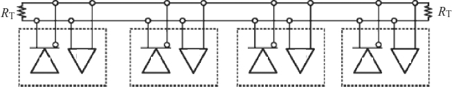
Figure 12.6 Multipoint configuration with a differential driver/receiver
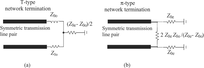
Figure 12.7 Optimal termination for a symmetric transmission-line pair: (a) T-type network termination; (b) π-type network termination
For a symmetric transmission pair, both even and odd modes of propagation should have a termination equal to the characteristic impedances Z0e and Z0o, respectively, to avoid any type of reflection. This can be accomplished by either a π-type network [1] or by a T-type network, as shown in Figure 12.7.
However, as previously discussed, differential pairs are not typically terminated with the networks in Figure 12.7. Three common termination schemes used in practice are shown in Figure 12.8. The bridge solution (Figure 12.8a) provides termination without reflections for differential mode, while the even or common mode is completely reflected. Examples of signaling with this solution are given in Section 9.7.2. This means that common-mode disturbances such as external interfering fields or ground loop coupling noises (see Section 10.1) can cause common-mode oscillations on account of the fact that the even or common mode is not properly terminated. This should not be a problem as long as there is no mode conversion and the differential receiver has sufficient common-mode rejection. The single-ended termination (Figure 12.8b) offers the advantage of matching the odd mode and partially the even mode. The drawback is that an extra resistor is required. A mix solution with a bridge at the receiver location and a single-ended termination at the differential driver offers a matched condition for the odd mode at both ends, while the driver damps the even mode, mitigating the common-mode noise produced by external interferences. The AC termination (Figure 12.8c) has the same advantages as the single-ended termination without increasing static power dissipation. The drawback is that a capacitor is required as a third element.

Figure 12.8 Termination schemes used in practice for a differential transmission-line pair: (a) bridge; (b) single-ended; (c) AC

Figure 12.9 Solutions to enhance EMI performance of a differential link communication by an unshielded twisted pair: (a) EMI filters at driver location to mitigate emission; (b) EMI filters at receiver location to increase common-mode rejection
Differential transmission is often used to link PCBs sharing different racks or equipment as a lower-cost solution with respect to coaxial cables. For economic reasons, the cable is often an unshielded twisted pair (UTP) of categories 3, 5, 5e, 6, and 7, depending on the speed of the transmitted signal [2]. The main problem with these types of cable is that, although cables 5e, 6, and 7 are well balanced, the radiated fields produced by the common-mode current, generated by the non-balanced condition of the switching edges within the differential driver, dominate over the radiated fields produced by the differential mode, as explained in Section 9.7.2, where the performances of RS422, LVDS, and LVPECL drivers are compared. It is shown that, without EMI filters, the emission profile can be higher than the emission limit imposed by the CISPR 22 standard for 3 m Class B equipment. An EMI filter useful for mitigating emission is the one indicated in Figure 12.9a, where the transformer followed by a common-mode choke has the task of stopping the common-mode current, and the capacitor connected to the central point of the transformer has the task of diverting the common-mode current to the ground of the PCB. Reducing the common-mode current leads to minimization of cable emissions. The efficiency of this type of EMI filter is shown in Section 10.3.4, where several grounding solutions are also compared using a 3D numerical code. To increase significantly the immunity of the receiver to common-mode noises, the same EMI filter solution should be implemented at the receiver location as indicated in Figure 12.9b. The capacitors with the task of diverting the interfering common-mode current should be connected to a PCB clean ground connected to the chassis with a very low impedance. How these filters act in improving the common-mode rejection of the receiver will be explored in Example 12.1 by measurements. Note that in Figure 12.9 the traces used to connect the components with the cable connectors must have an impedance of 50 Ω in order to have a differential impedance of 100 Ω, which matches the 100 Ω characteristic impedance of the UTP cables.

Figure 12.10 Output equivalent circuit of an LVDS device driving a line terminated with a resistance
Moreover, the traces must be symmetrically positioned with respect to all nearby grounded objects.
12.1.5 LVDS Devices
LVDS features a low-swing differential constant current source configuration that supports fast switching speeds and low power consumption [12]. The configuration is shown in Figure 12.10. The output equivalent circuit of the LVDS device is a current source with high impedance that provides termination resistance RT with a typical 3.5 mA current for one logic state and a typical −3.5 mA current for the other logic state. This means that the receiver sees a differential signal of 2 × 350 = 700 mV.
Differential signaling also offers common-mode rejection. The receiver ignores any noise that is coupled equally with the differential signals and considers only the difference between the two signals. The receiver has a common-mode voltage in the range 0.25−2.25 V. LVDS receivers will operate with as much as a ±1 V ground shift between driver and receiver, as shown in Figure 12.11.
Failsafe is a feature offered in LVDS that will help system reliability by preventing errors. Failsafe guarantees that the outputs are in a known state (high or low) when the receiver inputs are under certain fault conditions. Without the failsafe feature, any external noise above receiver thresholds could trigger the output to an unknown state. With the failsafe feature, the receiver outputs will always be in a known state as long as the inputs are not receiving a valid signal.
Example 12.1: LVDS Signal Integrity and Common-mode Rejection Investigation by Measurements
Two test boards with LVDS devices were built in order to check signal integrity in serial link and immunity to common-mode disturbances. To carry out the test, commercial devices satisfying the LVDS standard were chosen according to the set-up shown in Figure 12.12, where:
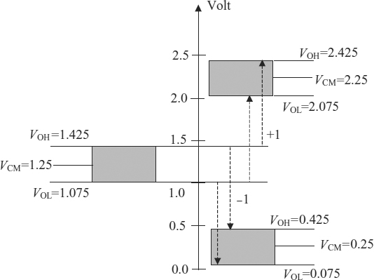
Figure 12.11 LVDS common-mode noise range
- DS90LV31A is one buffer with TTL-compatible input and differential LVDS output, characterized by a clock frequency fclock = 200 MHz and an NRZ data sequence.
- DS90LV32A is one buffer with a differential LVDS input and a TTL-compatible output.
- The cable is a 100 Ω UTP of Cat-5e with the drain wire connected to the ground board (GND_TX, GND_RX) and length lcable = 10 m.
- Traces on the board have a differential characteristic impedance of 100 Ω.
- The connectors are of type Z-pack.
- The termination resistance RT = 100 Ω.
With this structure, the ground noise between the two boards should be less than 1 V. To allow a greater noise level than 1 V, decoupling capacitors and impulse transformers with common-mode chokes should be used.
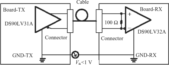
Figure 12.12 Test set-up for common-mode rejection in an LVDS serial link

Figure 12.13 Measured eye diagrams for the basic link
Signal Integrity
The signal integrity was investigated by performing eye diagram measurements on the basic configuration in Figure 12.13 and on four other configurations shown in Figure 12.14. The jitter value was calculated between the thresholds ±100 mV and given in histogram form (just below the eye diagram of Figure 12.13). Measurements on a direct link using a 100 nF capacitor to provide a partial match condition for common-mode disturbances are shown in Figure 12.13. In this case, the differential signal is matched with 2 × 50 = 100 Ω and the common-mode disturbances are partially matched by 50 Ω termination resistors connected to ground by the 100 nF decoupling capacitor.
Looking at the other configurations shown in Figure 12.14, the following comments can be made. The decoupling action of the series capacitors has the purpose of increasing the basic value of ±1 V as immunity to common-mode noise. In this case, it is necessary to provide a polarization voltage of 1.2 V at the receiver by a resistive net. The central point of the transformer is connected to ground by a 100 nF capacitor to divert to ground the common-mode noise. The choke has the task of stopping the common-mode noise passing through the parasitic capacitances between the two coils of the transformer.
In all the cases investigated, it was verified that the signal at the receiver is characterized by an open eye diagram, symmetric with respect to the 1.2 V voltage, and with a clear crossing between the differential decision thresholds of ±100 mV. The jitter values of the different solutions are summarized in Table 12.1.
Common-mode Immunity
For the purpose of investigating how EMI filters such as decoupling capacitors, transformers and common-mode chokes enhance the immunity of receivers to common-mode disturbances, the set-up shown in Figure 12.15 was realized. The measurements were carried out under the following conditions:
Figure 12.14 Configurations: (a) transformer and CM choke at receiver end; (b) capacitors at receiver end; (c) transformer and CM choke at driver end; (d) capacitors at driver end
- clock signal;
- noise amplitude 0–50 V;
- noise pulse duration 80 μs;
- trigger given to the oscilloscope by the noise generator;
- all measurements have ground 2 of the receiver as the reference point.
When the noise is applied, the isolation transformer acts like the wire drain of the cable. For this reason, during this type of test, the wire drain of the cable was disconnected from the board ground.
Table 12.1 Jitter of LVDS links

Figure 12.15 Set-up for immunity noise measurements between two grounds of the LVDS link
The waveform of the impulse noise depends on the type of load applied to the source. An example of noise without load is shown in Figure 12.16. The duration of the pulse was always set to 80 μs.
Without the drain wire connected to both board grounds, the common-mode noise at point CM of Figure 12.13 follows the induced noise at point B of Figure 12.15 between the two grounds (same waveforms). There is a loss of data for a voltage noise of the generator of 2 V.
With 220 nF decoupling capacitors at the receiver end, the noise generator is connected to a circuit with high impedance. The noise at point CM is lower than the noise at point B. Data failure occurs with low values of the noise generator, i.e. with a voltage at point B of about 4.6 V, with a slight improvement in immunity, of about 2.5 V. Loss of data also occurs with decoupling capacitors at the driver end with less immunity. The results obtained are summarized in Table 12.2.
With a transformer and a common-mode choke at the receiver or driver end, no data failure was recorded, even in the case of a 40 V voltage noise assigned to the source noise generator. In this case, noise at point CM is also very low for high values of voltages at point B.
The immunity to common-mode noise voltages of LVDS devices was checked, considering the basic link of Figure 12.13 without the presence of the drain wire. The signal voltage VA at the receiver output at point A and the applied noise voltage VB at point B increased gradually from 0 V to 15 V where monitored, and the results are shown in Figure 12.17. In particular, in graphs 1 to 9 the following situations can be observed:
1. Regular signaling without noise.
2. Signal with one single error due to noise.
3. Signal with several errors.
4. The driver returns to transmit when the noise ceases.
5-8. There is an advanced change in the device characteristics with increasing applied voltage noise. The impedance seen by the noise source decreases, as can be seen from the deformation of the impulse noise from a trapezoidal shape to a form with steps.
9 The driver stops transmitting. The data transmission is correct again only after switching the power supply off and on in sequence, and in the absence of noise. This behavior of the driver was verified with a noise voltage of up to 40 V.

Figure 12.16 Output voltage of the noise generator without load
Table 12.2 Maximum peak noises that cause data failure with decoupling capacitors in the LVDS data link
To check the breakdown of LVDS devices in the static condition, a DC voltage source was connected directly without an isolation transformer to the two ground boards in Figure 12.15. The drain wire of the cable was not connected to the two grounds. Three drivers and receivers were used for the test. The noise voltage VnDC was slowly varied from 0 to 9.5 V.
Breakdown did not occur suddenly but after the following stages:
- VnDC = 0−2.4 V, the link worked correctly.
- 2.4 V < VnDC < 8.5 V, data transmission was interrupted, but, by decreasing the offset voltage, it was corrected again;
- VnDC = 8.5–9.5 V, the device broke down (the drivers twice and the receivers once).
After these experiments, it can be concluded that:
- No failures on the data stream were observed with the drain wire connected, which high-lights the importance of this connection for receiver immunity.
- With a direct link, without drain wire, data failures were observed at a noise voltage of about 2 V. Common-mode voltage at the receiver has the same waveform of the impulsive noise applied between the two PCB grounds.
- With decoupling capacitors of 220 nF and without drain wire, the noise peak of 3.5–4 V can cause data failure. The series capacitor is useful when the offset voltage remains constant. Common-mode voltage at the receiver has a smaller peak value than the applied impulse noise.
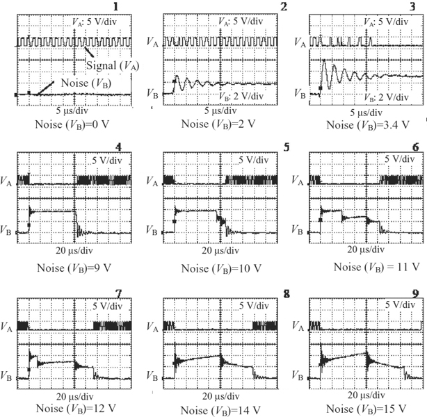
Figure 12.17 Signal interruption during a noise impulse with the basic link without drain wire: 1, signal without noise; 2, one bit error; 3, several bit errors; 4, transmission becomes regular when the noise application ends; 5–8, the devices change their characteristics with increasing noise level; 9, the driver stops working and transmits again after the return of power supply
- With a transformer and common-mode choke, and without drain wire, no data failures were observed with high-noise voltage up to 40 V.
- With static noise, breakdown of the LVDS devices can occur with a noise voltage of 8 V.
- Jitter increases slightly when a transformer and common-mode choke are used.
As recommendations for maximum noise immunity when using Unshielded Twisted Pairs (UTPs):
- Links with a transformer and common-mode choke should be used.
- The drain wire of the UTP cable must be connected to both grounds at both ends.
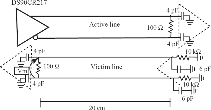
Figure 12.18 Two coupled pairs of differential lines with LVDS equivalent circuits for crosstalk investigations
Example 12.2: LVDS Crosstalk Investigation by Simulations
Performing simulations is the best way to set design rules for routing differential traces in PCBs. In the following, the spacing between two pairs of traces is investigated, considering their relative position.
The circuit model analyzed by the HSPICE simulator was carried out by simulating the lines with the distributed models presented in Section 6.4, and computing the per-unit-length line parameter with a field solver. DC and skin-effect losses in traces were accounted for. Dielectric losses were neglected, as the interest was focused on the maximum-level crosstalk at the near end (NEXT). The length of the lines was chosen to permit crosstalk to rise to its maximum value, and the orientations of the driver and receiver were chosen to simulate the worst case. The simulated PCB structure is typical of an actual design.
The adopted topology in the case of two differential lines with LVDS devices is shown in Figure 12.18. The driver in the active line was simulated by a macromodel of the DS90CR217 device, starting with the IBIS model provided by the manufacturer (The National Semiconductor). The rise and fall times of the driver tr = tf = 700 ps were computed between 10 and 90 % of the 700 mV swing. In the victim line, the driver is represented with a high impedance (10 kΩ between the two traces and 6 pF connected to ground) for the purpose of avoiding results dependent too much on a particular device and for better reproducibility. For the same reason, the receiver was simulated by two 4 pF capacitors connected to ground. The length of the lines was 20 cm and the differential traces were matched at the receiver end by a 100 Ω resistance.
Simulations were performed by considering several locations of the traces, as shown in Figure 12.19a. In the base configuration indicated by ‘0’, the couples of traces for differential signaling had a width w = 0.2 mm, a thickness t = 0.018 mm, and a separation s = 0.2 mm. Adopting a relative dielectric constant εr = 4.3, the characteristic differential impedance is about 100 Ω. The simulated waveforms of the near-end crosstalk are shown in Figure 12.19b for a driver switching frequency of 33 MHz. The results refer to structures in which a couple of traces are kept at the same location while the other is horizontally shifted with a step equal to the width of the trace. Observe that the waveforms 0 and 1 in Figure 12.19b have opposite sign to the each other. This is due to the fact that, for configurations 0 and 1, conductor p of the first pair of traces is mainly coupled with conductor p of the second pair of traces. For the other structures, the coupling between conductor p and conductor n is dominant. However, this fact is not so important, as the purpose is to reduce the crosstalk magnitude.
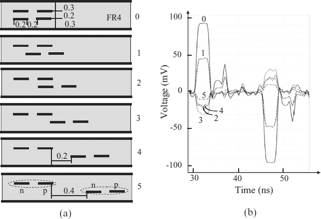
Figure 12.19 Crosstalk with LVDS: (a) PCB structures with dimension in mm; (b) Vm simulated waveforms by SPICE (see Figure 12.18)
Another case of practical interest is the crosstalk between coplanar differential pairs with LVDS devices, as shown in Figure 12.20. There are two active lines disturbing a victim line in the middle. The receiver of the victim line is located at the same end as the drivers. Simulations with the receiver at the opposite end did not provide significant differences.
The basic structure is shown in Figure 12.21a, where the separation parameter s was varied. The results of the simulations are shown in Figure 12.21b. It was verified that the presence of a second active line doubles the crosstalk. Considering this fact, the case s = 0.2 mm provides a maximum crosstalk similar to case 4 in Figure 12.19a. For s = 0.6 mm, and considering one driver, the crosstalk is 0.5 × 10/700 × 100 = 0.7 %. Making s = 0.9 mm as in Figure 12.3, the target of 0.2 % is obtained.
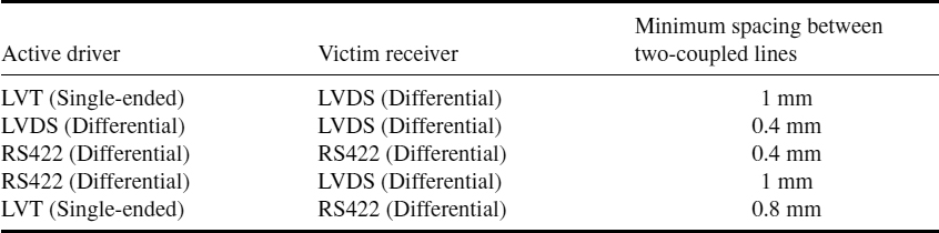
Other simulations of coplanar traces with different logic families led to the rules for minimum spacing shown in Table 12.3. The values reported ensure that crosstalk is a reasonable part of the total immunity of the receiver. Structure with parallel overhead traces in two adjacent layers must be absolutely avoided owing to the high level of crosstalk. Other information for signal integrity interconnect can be found in reference [24].
Example 12.3: Characterization of a Backplane for High-speed Application up to 3.125 GHz by Measurements
In this example, the experimental characterization of a backplane to verify the compliance with the AdvancedTCA requirements will be described. The backplane should meet the following specifications:

Figure 12.20 Three coupled pairs of differential lines with LVDS equivalent circuits for crosstalk investigations
- Maximum data rate 3.125 GHz.
- The differential impedance of the backplane serial links for the high-speed interfaces shall be 100 Ω ± 10 %.
- The backplane signal lengths, within the differential pair, shall be matched better than 3.4 ps (0.5 mm separation between the two ground planes and FR4 at εr = 4).
Figure 12.21 Crosstalk with two active LVDS devices and one victim line: (a) PCB structures with dimensions in mm; (b) Vm simulated waveforms by SPICE (see Figure 12.20)
Table 12.3 Minimum spacing between two coupled lines as a function of the technology
- The transmitting and receiving pairs within a fabric channel routed across the backplane shall have a delay time in matched condition of 17 ps or less (0.254 mm trace separation in FR4 at εr = 4).
- Crosstalk lower than 0.2 % (near-end coupling coefficient NEXT) for a pair of traces with a separation of 0.889 mm (edge to edge).

The physical stack-up of a 14-layer motherboard is shown in Figure 12.22a. The notation GND means a layer dedicated to ground, POWER means an area of the plane dedicated to the power supply, and HFi means layer i dedicated to traces, with i = 1,2,…, 6. The geometries of a pair of traces for differential transmission are chosen according to the ATCA requirements (see Figure 12.22b) in order to have an odd characteristic impedance Z0o = 50 Ω and therefore a differential characteristic impedance Z0DM = 2Z0o = 100 Ω.
Three types of measurement were carried out:
- TDR measurements to verify the required characteristic impedance;
- TDR measurements to verify the crosstalk;
- oscilloscope measurements to verify the jitter
For all the measurements, a commercial test board, referred to as the test blade, was used to connect the motherboard with the instruments, as shown in Figure 12.23a. The test blade is an off-the-shelf ATCA solution designed by NESA and F9 Systems [24] for measurements up to and including 10 Gbps. It is particularly suitable to monitor the active transmission and received signals across an ATCA backplane to assure signal quality, to measure impedance and coupled Near End Crosstalk (NEXT), to measure skew and propagation delay. SMA connectors assure the connection between the traces and the instruments, as shown in Figure 12.23a.
To verify the odd impedance Z0o of each trace of a differential interconnect, it is necessary to perform differential TDR measurements in order to excite both traces at the same time with complementary steps of amplitude 250 mV and a rise time of 25 ps, as shown in Figure 12.23b. The results of differential TDR measurements are shown in Figure 12.23c, where it can be noted that, for both traces in the test blade and in the backplane, the required odd impedance Z0o = 50 Ω is verified, as the reflected waveforms for the two boards are very low considering the 50 Ω reference waveform of the TDR. Some inevitable slight distortions can be observed owing to the SMA and daughter–motherboard connectors. The delay time of the 20 cm trace can be deduced by examining the time interval between the blade connector and the moment when the waveform rises to high values, as the incident step sees an open line. In fact, this time is twice the time required by the TDR step to go from the connector to the open end of the trace. This delay being about 2.5 ns, the per-unit-length delay time of the trace is tpd = (2.5/2)/0.2 = 6.25 ns/m.

Figure 12.22 Example of a 14-layer board in FR4, thickness t = 3.472 mm ± 10 %: (a) stack-up; (b) details of differential traces for a differential characteristic impedance Z0DM = 100 Ω (courtesy of Dr Vittorio Ricchiuti, Technolabs, Italy)
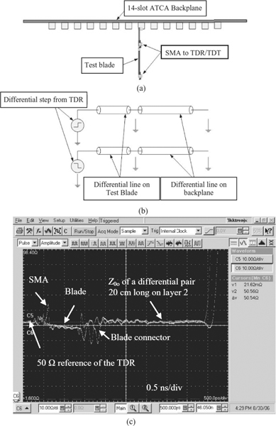
Figure 12.23 TDR measurements: (a) view of test board and backplane; (b) schematic of TDR and traces; (c) measured TDR waveforms showing that each trace for differential transmission has an odd characteristic impedance Z0o = 50 Ω (courtesy of Dr Vittorio Ricchiuti, Technolabs, Italy)
Owing to its complementary outputs, the differential TDR is also suitable for crosstalk measurements, as shown in Figure 12.24a. The equivalent circuit is shown in Figure 12.24b.
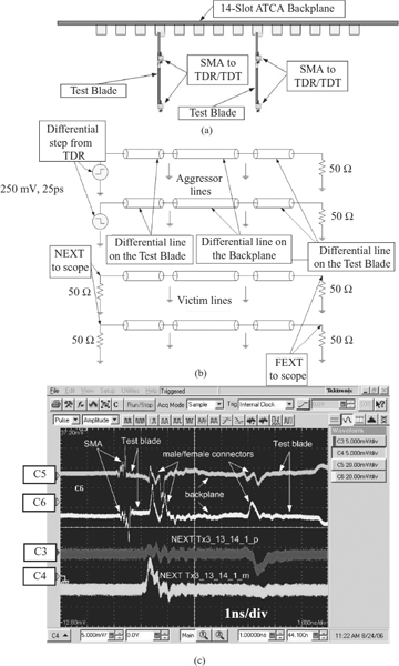
Figure 12.24 Crosstalk measurements: (a) view of test boards and backplane; (b) schematic of TDR and coupled traces; (c) measured waveforms showing distortions on aggressor lines owing to SMA and male/female connectors and near-end (NEXT) crosstalk on victim line (courtesy of Dr Vittorio Ricchiuti, Technolabs, Italy)
Of course, the two test boards have isolated pairs of traces for differential signaling. Therefore, the single-ended NEXT waveforms of Figure 12.24c concern the traces on the backplane only. As each trace is matched by its characteristic impedance, according to crosstalk theory, discussed in Section 6.1, NEXT should have a width equal to twice the delay time of the trace of 26 cm length in the backplane (i.e. 2 × 6.25 × 0.26 = 3.25 ns), and a rise/fall time of 25 ps. With the scale adopted for waveforms c3 and c4 (i.e. 5 mV/div and 1 ns/div, as shown in Figure 12.24c), the crosstalk waveforms are flat, and therefore the requirement of <0.2 % crosstalk is satisfied. The peaks of about 5 mV and of less than 1 ns width are due to a slight mismatch at the connector, as evidenced in waveforms c5 and c6 of the aggressive line.
Eye diagram measurements are shown in Figure 12.25. In this case, one test blade is used to launch signals generated by pattern generators, and the other board is used to monitor the waveforms at the end of the pair of differential lines (see Figure 12.25a). The location of the differential line under test in the motherboard is shown in Figure 12.25b. Measured eye diagrams are shown in Figure 12.25c. Observe that the peak-to-peak jitter tcs/tui × 100 = 40/320 × 100 = 12.5 % is suitable for this type of frequency and application, as the eye is evidently open.

Figure 12.25 Eye diagram measurements: (a) view of test boards and backplane; (b) backplane layout; (c) measured waveforms at pattern generator location and at the output of the test blade (courtesy of Dr Vittorio Ricchiuti, Technolabs, Italy)
12.2 Modeling Packages and Interconnect Discontinuities in PCBs
In this last section of the book, the problem of how to extract equivalent circuits to simulate discontinuities in PCBs with SPICE is considered. These models can be used for simulating reflections and for computing extra delays along an interconnect with several discontinuities. Very useful tools for extracting the fundamental parameters for the model are those based on full-wave numerical solutions of field equations. Some examples are provided. The section ends with a brief discussion concerning the types of package used for digital devices in order to minimize the parasitic effects of their connections to the PCB.
12.2.1 Multilayer Boards
Discontinuities in a multilayer PCB such as bends, vias, connectors, IC packages, ground gaps, etc., should be simulated with an appropriate equivalent circuit to investigate their effects on signal integrity and how they generate EMI [25]–[28]. Every layout discontinuity must be properly accounted for, performing the simulations of the full interconnect including suitable macromodels of drivers and receivers, especially for high-speed differential transmission [29, 30]. Of particular importance are the discontinuities affecting current return paths of the signals. They have inductive effects, and the consequences are:
- to slow the edge rate by filtering out high-frequency components;
- signal integrity problems at the receiver if the current divergence path is long;
- to increase the current loop area and then EMI;
- to increase the coupling coefficient between signals.
Bends, vias, and connectors have complicated structures, and three approaches can be used for modeling their effects:
- Transmission-line models.
- Lumped-circuit elements.
- Full-wave analysis and scattering responses.
Choice 1 is difficult to realize, which practically means no models. Choice 2 is the most useful for qualitative assessments. Choice 3 should be applied when an accurate equivalent circuit of the discontinuity is required for SPICE simulations. The equivalent circuit should reproduce the S-parameters computed by the full-wave code [31]–[33] or measured directly by a Vector Network Analyzer (VNA). Some examples of these procedures will be provided in this section.
12.2.2 Bends
Bends in a real PCB are necessary owing to the high density and consequently routing constraints regarding traces. An example is shown in Figure 12.26a. A lumped model for a bend is a shunt capacitor, as shown in Figure 12.26b. It has been demonstrated through correlation with empirical measurements that a simple lumped-capacitance model is adequate for most systems [34]. The value of the bend capacitance Cbend is
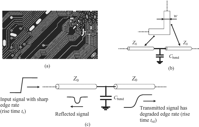
Figure 12.26 Bends: (a) example in a PCB; (b) equivalent circuit; (c) rise time degradation
where C = tpd/Z0 is the per-unit-length line capacitance, w is the width of the strip, and tpd and Z0 are respectively the per-unit-length delay time and the characteristic impedance of the trace forming the bend. For a 90° bend the capacitance value is equal to that of a transmission-line segment equal to its width or, in other words, it is the capacitance of the square portion of trace area that joins the two vertical traces forming the bend. Although this capacitance is small, it can cause signal integrity problems if several bends are present along the trace. A good solution for mitigating bend effects significantly is to chamfer the edge by 45°, as shown in Figure 12.26a. The capacitance of a 45° bend is significantly smaller than that of a 90° bend. Figure 12.26c illustrates how the signal rise time is changed by the bend according to
where tbend takes into account the effect of the shunt capacitance Cbend.
For a more accurate assessment of signal integrity regarding bends, a 3D simulation is the most appropriate tool, especially when other phenomena such as coupling between the same trace occurs, as will be shown with the serpentine example in the following section.
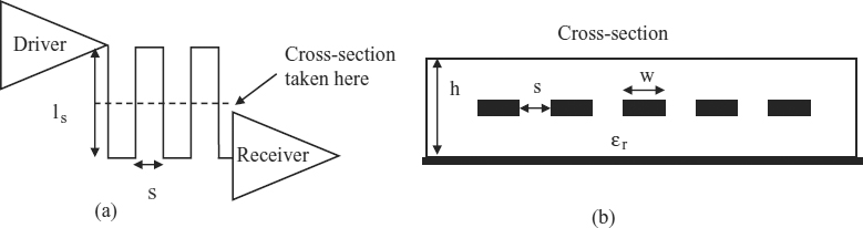
Figure 12.27 Serpentine: (a) routing; (b) cross-sectional view
12.2.3 Serpentines
Usually, in actual PCBs, it is not possible to route a trace in a perfectly straight line in order to have a well-controlled characteristic impedance and delay time. Board constraints such as geometries, high density layout, and timing requirements force the traces to be routed in serpentine patterns, as illustrated in Figure 12.27a. For timing reasons, serpentine traces are also often used to delay the data with respect to the clock in order to enhance the hold time, or to equalize trace lengths.
Care must be taken in routing the trace, as parallel sections could be coupled, causing signal integrity problems and EMI effects. The design rules to follow can be summarized as follows [34]:
- A spacing s greater than 3–4 times the substrate height h should be used.
- The length ls of parallel sections should be minimized.
- Serpentines should be avoided in the case of clock signals.
12.2.4 Ground Slot
In actual PCBs it is not rare for a trace with the structure of a microstrip to have to cross a gap in the return ground plane, as shown in Figure 12.28. A slot in the ground adds inductance to a trace passing perpendicularly over the slot, creating signal integrity and EMI problems [35, 36]. As shown in Figure 12.28, the return current from the driver cannot flow directly under the trace but diverts around the ends of the ground slot. Only a little portion of the return signal current flows through the gap capacitance. The diverted current flows on a large loop and greatly increases the inductance of the signal path. The effective inductance associated with the gap can be considered in series with the trace, and it can be estimated approximately using the expression of a loop formed by two flat parallel conductors with center-to-center distance d, and having width w and length l. Assuming that the return current around the gap flows onto two parallel conductors of width w = 3wt and length l = D, and spaced by d = wc + 3wt, the inductance associated with the gap according to Table A2 of Appendix A is

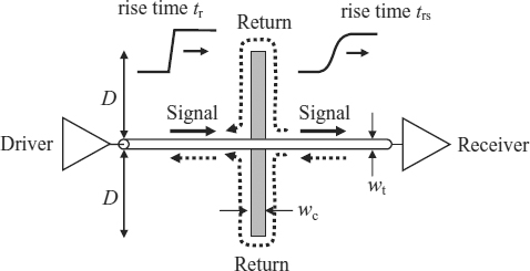
Figure 12.28 Current paths in a slotted ground plane and signal rise time degradation
where tt is the thickness of the trace. In Equation (12.4), the factor 1/2 is added to take into account that the slot causes the effect of two loop inductances in parallel, and factor 2 takes into account that we are interested in calculation of the inductance of one of the loops which is twice the effective inductance associated with one branch of the loop. In this calculation, for simplicity, the edge effects are neglected.
Example 12.4: Numerical Simulation of the Distortion Introduced on Signals by a Slot in the Ground Plane
To validate the slot inductance expression (12.4), numerical computations were performed for the test PCB shown in Figure 12.29a by using MWS [22]. The test PCB has the dimensions 20 mm × 100 mm × 0.77 mm and a thickness of the dielectric layer of 0.7 mm, with εr = 4.4, wt = 0.35 mm, tt = 0.035 mm, trace length l = 100 mm, a gap created in the middle of the PCB of size D = 7.5 mm, and wc = 5 mm (see Figure 12.28 for the notation of different parameters). The source was an ideal voltage source with a trapezoidal waveform of 1 V amplitude, rise and fall times tr = tf = 0.1 ns, pulse width tpw = 5 ns, and ttot = 10 ns. The trace was loaded with its characteristic impedance Z0 = 90.36 Ω. Introducing these values in Equation (12.4) yields Lslot = 4.82 nH. This is a high value that produces significant distortion on the signal line and increases common-mode emission, especially when a cable is attached to the PCB; recall that a typical effective inductance associated with a ground plane is less than 1 nH for actual PCBs having the traces close to its reference plane (see Chapter 9).
It is interesting to look at the surface current distribution around the slot, computed by MWS at 1 GHz and shown in Figure 12.29b. Note that the assumption adopted in Equation (12.4) that most of the return current concentrates in a space equal to 3wt is realistic.
The comparison between waveforms obtained by SPICE and MWS is shown in Figure 12.30, where a good agreement can be observed for two kinds of slot having different width wc. These results confirm the validity of Equation (12.4). For a gap of 5 mm there is a negative reflection of 25 % of the signal. This signal distortion cannot be tolerated in a highspeed digital system, and a trace crossing a gap must be absolutely avoided. If routing a trace across a gap cannot be avoided, a stitching capacitor placed across the gap and close to the signal trace can be a solution to overcome this problem. However, this fix cannot always be realized.
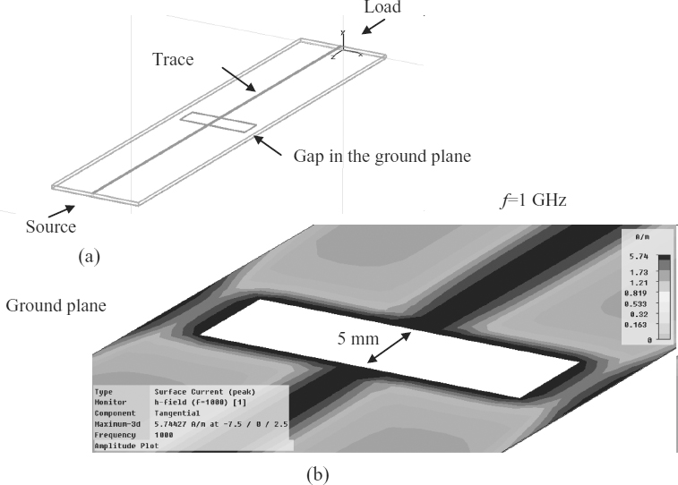
Figure 12.29 PCB with a gap in the ground plane: (a) PCB structure modelled by MWS; (b) tangential surface current plot in proximity of the gap at 1 GHz
A good solution is to use differential transmission. Simulations by MWS were performed for the PCB structure shown in Figure 12.31a, where a second trace was added to the PCB of Figure 12.29a to form a differential line. The separation between the two traces (edge to edge) was s = 0.65 mm. Two ideal voltage sources having complementary waveforms were used to excite the traces with equal but opposite currents. The load was a resistance between the end of the pair traces with value Z0DM = 200 Ω. In fact, to have a perfect matching, the load should be equal to twice the odd characteristic impedance of two symmetric coupled lines. Note that, with a differential transmission, the negative reflection is a very low percentage of the signal. This confirms an assertion made in Section 10.3.4: to increase the efficiency of a common-mode choke used as an EMI filter, the reference area between the device and the connector could be removed in the case of differential transmission. This fix lowers the parasitic capacitances, which could create an alternative path between the traces before and after the filter. The best performance of differential transmission over single-ended transmission is seen when the reference plane for return current is not solid. This is also confirmed by the investigation reported in reference [44] on PCBs with the power plane having a planar Electromagnetic BandGap (EBG) structure for mitigating simultaneous switching noise propagation. In reference [44] it is shown that an eye diagram with differential transmission is significantly better than that obtained with single-ended transmission for EBG structures.

Figure 12.30 Simulated waveforms when a ground plane has a gap: (a) equivalent circuit for SPICE; (b) results with a gap having wc = 5 mm; (c) results with a gap having wc = 1 mm
To conclude this section, for single-ended connections the degradation of the signal rise time can be computed as
12.2.5 Vias
A via is the way to connect two traces belonging to different layers of a PCB or to connect components to traces [34]. Figure 12.32a shows an example of a via connecting a trace on layer 1 with a trace on layer 2. The via consists of the barrel, the pad, and the antipad, as depicted in Figure 12.32b. The barrel is a conductive material that fills the hole to permit an electrical connection between layers, the pad is used to connect the barrel to the trace component, and the antipad is a clearance hole between the pad and the metal plane on a layer to which connection is not required. The via could be of the through-hole type because it is made by drilling a hole through the board. Other vias are blind, buried, and microvias (see Figure 12.32a for examples). When the maximum dimension of a via is much less than the minimum wavelength of interest, or, in other words, is electrically short, the via can be represented by the π-net circuit of Figure 12.32c. The capacitors represent the via pad capacitance on layers 1 and 2. The series inductance represents the barrel. The capacitance [37] and the inductance (see the isolated wire in Table A.1 of Appendix A) can be estimated by the following closed-form expressions:
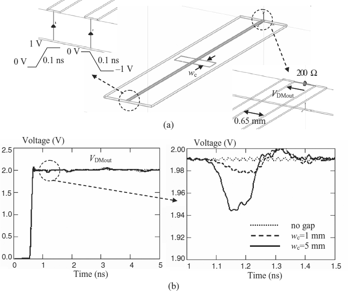
Figure 12.31 Simulated waveforms when a ground plane has a gap and the signal transmission is differential: (a) MWS model of the structure; (b) voltage VDMout on the load without a gap, with a gap having wc = 5 mm and wc = 1 mm

where d1 is the via barrel diameter, d2 is the via pad diameter, t is the distance between the pad and the nearest reference plane, h is the via length, μ0 = 4π10−7 H/m, and the length must be in meters.
However, the best way to extract an equivalent circuit of a via is to calculate S-parameters by using a 3D numerical code and compare the results with an equivalent circuit implemented in SPICE. This procedure is explained by Example 11.4 in Section 11.2.3, where the validation limit of the π-model is also discussed. More accurate procedures for characterizing vias can be found elsewhere [38–40]. It is important to point out that the inductance computed by Equation (12.6b) refers to an isolated round wire, and it is this value that mainly deteriorates the signal integrity. The effective inductance associated with the via can be lowered if the return signal current flows in a via close to the signal via, as explained in Section 10.2.3. In fact, the mutual inductance between the vias has a positive action, as it must be subtracted from the self-inductance of the signal via to calculate the effective inductance associated with the via. This can be accomplished by taking care to place a decoupling capacitor in a manner such that its via, connecting the capacitor to the ground or power plane of interest and acting as signal return current, must be close to the signal via. If this does not occur, because the signal current follows a return path with minimum impedance, the return current has two possibilities: one is the nearest via available for the return current, usually causing a large loop of current at low frequencies; the other is the displacement current between the planes crossed by the signal via, and this occurs when the frequencies are so high that the local capacitance between the plane allows the flow of the return current. Of course, since this last situation cannot be controlled, it should be avoided in order to minimize signal integrity and EMI problems.

Figure 12.32 Via: (a) cross-view of a via in a PCB; (b) 3D view; (c) equivalent circuit
12.2.6 Connectors
Connectors are components that are used to connect one printed circuit board to another. An example of a connector is shown in Figure 12.33. Note that the conductors of the connector have a complex geometry; they do not follow a straight path, and only those that share the same row have equal length. The ground pins are generally longer than the others for safety reasons. In fact, during the insertion of the PCB onto the powered system, it is essential that the ground pins of the PCB contact the ground system first to avoid damage. This makes modeling of the connector extremely hard without using measurements or 3D field solvers to extract a connector equivalent circuit. Good examples of connector modeling are given elsewhere [41, 42]. All the self and mutual inductances and capacitance parameters should be considered, as there are two problems in the connector: crosstalk among the pins and voltage drops on the ground and power pins owing to the return of the signal currents. In fact, the inductance associated with power and ground pins produces common-impedance coupling, as the return current of the signals shares the same ground and power pin.

Figure 12.33 Example of a connector for PCBs
This section presents an approximate approach for investigating connector problems, based on the fact that the capacitance effect can be neglected when the maximum dimension of the connector is electrically short. This can be done because the main effect of the connector capacitances is to slow down the system edge rate [34]. For this reason, the discussion will be focused on the inductance effects.
Consider the simple connector structure depicted in Figure 12.34a. The dominant effect of connectors is accounted for by a series-lumped self partial inductance given by the simplified expression (see Table A1 of Appendix A for an isolated wire)
and a mutual partial inductance between two pins given by the simplified expression (see Table A1 of Appendix A for two parallel wires with opposite currents)
where l is the length of the pin, r is the average radius of the pin, and s is the spacing between two pins. For s comparable with l, Mcon is given by the more complete closed-form expression of Table A.1 regarding two parallel wires.
These expressions can be used for segments of parallel pins (see Figure 12.34a and its equivalent circuit shown in Figure 12.34b). The shape of the connector pin is not relevant for modeling, and therefore an average pin radius can be adopted for calculations. The voltage drop on the ground pin caused by other n – 1 signal pins with current I, having the same self inductance and approximately the same mutual inductance, is

Figure 12.34 Connector: (a) two coupled pins; (b) equivalent circuit
The higher the coupling between signal and ground/power pins, the higher is the mutual inductance. As the self inductance of a pin is independent of the spacing between two coupled pins, a lower voltage drop Vgnd on the ground/power pins occurs. Therefore, this simple expression for Vgnd makes it possible to establish some fundamental design rules:
- The number of power/ground pins should be larger than the number of signal pins, which in practice means n = 1 in Equation (12.8).
- Signal pins should be close to their current return pins, which means high mutual inductance.
- Power and ground pins should be adjacent to maximize associated mutual inductance.
- Pin connectors should be ‘short’, as pin inductances depend on length l.
In Section 10.3, examples of ground noise calculation and SPICE simulations to explore EMI effects and deterioration in the signal integrity caused by common-mode coupling in the connector have been provided. Pin assignment for connectors with several pins has also been discussed.
Once all the self and mutual partial inductances are known by Equations (12.7), calculation of the voltage drop along each signal pin, useful for calculating crosstalk, can be done following the procedure outlined in Section 3.2.6, which links the concept of loop inductances with the concept of partial inductances.
In the case of differential transmission and the connector of Figure 12.33, it is very important to choose as pair pins two adjacent pins in the same row in order to avoid skew.
12.2.7 IC Package
Connections of chips to boards are also points of discontinuity [34]. Figure 12.35 shows two examples. Holders provide mechanical, thermal, and electrical connections of chips to boards.

Figure 12.35 IC package: (a) lead frame directly soldered on the PCB; (b) Pin Grid Arrays (PGAs) or Ball Grid Arrays (BGAs) stick out of the bottom of the package (as in the flip chip attachment) to a socket or to the board
They can be classified according to:
- type of die attachment;
- type of package connection;
- type of package attachment to board.
Some considerations about packages can be summarized as follows:
- Connection on packages can be routed via either controlled or non-controlled impedance traces.
- A controlled impedance package looks like a miniature multilayer PCB (it can accommodate more than one die).
- Non-controlled impedances are mostly used with wire bond attachment, where wires are directly connected to the lead frame (this means worse electrical performance).
Die attachment can be performed by wire bond or by the flip chip technique, as shown in Figure 12.36. A wire bond consists of a chip, mounted with pads on top, connected to the package by thin wires (~25 μm). The characteristics of the wire bond are:
- good mechanical and thermal connection;
- simple routing;
- large (and variable from wire to wire) series inductance;
- difficult to model.

Figure 12.36 Type of die attachment: (a) wire bond; (b) flip chip
Table 12.4 Inductances and minimum spacing between two coupled lines as functions of the technology
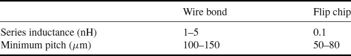
A flip chip consists of a chip mounted upside-down with pads on the bottom, which are connected to the package by solder balls. The characteristics of the flip chip are:
- worse thermal connection;
- finer pad pitch;
- smaller and predictable series inductance.
Typical electrical and geometrical parameters of the wire bond and flip chip are shown in Table 12.4.
Designers must be aware of package effects, which can be summarized as follows:
- Wire bond packages with lead frame attachment have the worst electrical performance, causing large series inductance and mutual inductances between wires, slow down edge rates, cause crosstalk, and exacerbate Simultaneous Switching Noise (SNN) effects.
- Wire bond packages with controlled impedance interconnects mainly cause a slower edge rate.
- Flip chip packages are mandatory for very high-speed applications.
- Parasitic circuit elements depend on the package shape and vary from pin to pin.
- Square packages minimize the mismatch of the parasitic elements of the pins.
When using IBIS models, make sure that the parasitic elements of the package are included. Further details about SPICE models of integrated circuits for EMI behavioral simulation can be found in the IEC 62433-2 standard [43]. The objective of this standard is to propose a model for describing the conducted emissions of an integrated circuit at the chip or multichip and PCB level and for power integrity analysis.
References
[1] Young, B., ‘Digital Signal Integrity: Modeling and Simulation with Interconnects and Packages’, Prentice Hall PTR, Upper Saddle River, NJ, 2001.
[2] Johnson, H. and Graham, M., ‘High-Speed Signal Propagation: Advanced Black Magic’, Pearson Education, Inc., Prentice-Hall PTR, Upper Saddle River, NJ, 2003.
[3] Thierauf, S.C., ‘High-Speed Circuit Board Signal Integrity, Artech House, Inc., Norwood, MA, 2004.
[4] Montrose, M., ‘EMC and the Printed Circuit Board: Design, Theory, and Layout Made Simple’, IEEE, Inc., New York, NY, 1999.
[5] Blood, W., ‘MECL System Design Handbook’, 4th Edition, Motorola Semiconductor Products, Inc., Phoenix, AZ, 1983.
[6] ‘Designing with PECL’, AN-1406, Motorola Semiconductor. Available online: www.freescale.com.
[7] ‘High-Speed Layout Design Guidelines’, AN-2536D, Motorola Semiconductor. Available online: www.freescale.com.
[8] ‘LVDS Owner s Manual’, National Semiconductor, Spring 1997. Available online: www.national.com.
[9] ‘A Comparison of Differential Termination Techniques’, AN-903, National Semiconductor. Available online: www.national.com.
[10] ‘Summary of Well Known Interface Standards’, AN-216, National Semiconductor. Available online: www.national.com.
[11] ‘Transmission Line Drivers and Receivers for TIA/EIA Standards RS-422 and RS-423’, AN-214, National Semi-conductor. Available online: www.national.com.
[12] ‘LVDS Description and Family Characteristics’, MS500530, Fairchild Semiconductor. Available online: www.fairchildsemi.com.
[13] ‘LVDS Reduces EMI’, AN-5020, Fairchild Semiconductor. Available online: www.fairchildsemi.com.
[14] ‘LVDS Fundamentals’, AN-5017, Fairchild Semiconductor. Available online: www.fairchildsemi.com.
[15] High-speed Differential Data Signalling and Measurements, AN, Tektronix, 2003. Available online: www.tektronix.com.
[16] AdvancedTCA, ‘Base Specification, PICMG_3_0_R2.0. Available at: www.picmg.org.
[17] Leone M. and Navratil V., ’On the External Inductive Coupling of Differential Signaling on Printed Circuit Boards’, IEEE Trans. on Electromagnetic Compatibility, 46(1), February 2004, 54–61.
[18] Kam, D., Lee, H., and Kim, J., ‘Twisted Differential Line Structure on High-speed Printed Circuit Boards to Reduce Crosstalk and Radiated Emission’, IEEE Trans. on Advanced Packaging, 27(4), November 2004, 590–596.
[19] Shiue, G.-H., Guo, W.-D., Lin, C.-M., and Wu, R.-B., ‘Noise Reduction Using Compensation Capacitance for Bend Discontinuity of Differential Transmission Lines’, IEEE Trans. on Advanced Packaging, 29(3), August 2006, 560–569.
[20] ‘Electrical Characteristics of Low Voltage Differential Signalling (LVDS) Interface Circuits’, TIA/EIA-644, 1 February 2001.
[21] ‘Electrical Characteristics of Multipoint-Low-Voltage Differential Signalling (M-LVDS) Interface Circuits for Multipoint Data Interface’, TIA/EIA-899, 2 March 2000.
[22] www.cst.com.
[23] ‘GTLP: An Interface Technology for Bus and Backplane Applications'’, AN-1065, Fairchild Semiconductor. Available online: www.fairchildsemi.com.
[24] www.nesa.com and www.f9-systems.com.
[25] Fan, J., Drewniak, J., and Knighten, J., ‘Lumped-circuit Model Extraction for Vias in Multilayer Substrates’, IEEE Trans. on Electromagnetic Compatibility, 45(2), May 2003, 272–280.
[26] McGibney, E. and Barrett, J., ‘An Overview of Electrical Characterization Techniques and Theory for IC Packages and Interconnects’, IEEE Trans. on Advanced Packaging, 29(1), February 2006, 131–139.
[27] Wang, C.-L. and Wu, R.-B., ‘Modeling and Design for Electrical Performance of Wideband Flip-chip Transition’, IEEE Trans. on Advanced Packaging, 26(4), November 2003, 385–391.
[28] Eo, Y., Eisenstadt, W., Jin, W., Choi, J., and Shim J., ‘A Compact Multilayer IC Package Model for Efficient Simulation, Analysis, and Design of High-performance VLSI Circuits’, IEEE Trans. on Advanced Packaging, 26(4), November 2003, 392–401.
[29] Stievano, I., Maio, I., Canavero, F., and Siviero, C., ‘Parametric Macromodels of Differential Drivers and Receivers’, IEEE Trans. on Advanced Packaging, 28(2), May 2005, 189–196.
[30] Stievano, I., Maio, I., Canavero, F., and Siviero, C., ‘Reliable Eye-diagram Analysis of Data Links via Device Macromodels’, IEEE Trans. on Advanced Packaging, 29(1), February 2006, 31–38.
[31] Araneo, R. and Celozzi, S., ‘A General Procedure for the Extraction of Lumped Equivalent Circuits from Full-wave Electromagnetic Simulations of Interconnect Discontinuities’, Proceedings of 15th International Zürich Symposium on Electromagnetic Compatibility, Zürich, Switzerland, February 2003, 419–424.
[32] Araneo, R. and Celozzi, S., ‘Extraction of Equivalent Lumped Circuits of Discontinuities Using the Finite-difference Time-domain Method’, IEEE 2002 International Symposium on Electromagnetic Compatibility, Minneapolis, MN, August 2002, 119–122.
[33] Araneo, R. and Maradei, F., ‘Passive Equivalent Circuits of Complex Discontinuities: an Improved Extraction Technique’, IEEE 2005 International Symposium on Electromagnetic Compatibility, Chicago, IL, August 2005, 700–704.
[34] Hall, S., Hall, G., and McCall, J., ‘High-Speed Digital System Design – a Handbook of Interconnect Theory and Design Practice’, John Wiley & Sons, Inc., New York, NY, 2000.
[35] Chen, J., Shi, W., Norman, A., and Ilavarasan, P., ‘Electrical Impact of High-speed Bus Crossing Plane Split’, IEEE Symposium on Electromagnetic Compatibility, Minneapolis, MN, August 2002, 861–865.
[36] Kim, J., Lee, H., and Kim, J., ‘Effects on Signal Integrity and Radiated Emission by Split Reference Plane on High-speed Multilayer Printed Circuit Boards’, IEEE Trans. on Advanced Packaging, 28(4), November 2005, 724–735.
[37] Johnson, H. and Graham, M., ‘High-Speed Signal Digital design: a Handbook of Black Magic’, Prentice Hall PTR, Upper Saddle River, NJ, 1993.
[38] Cui, W., Ye, X., Archambeault, B., White, D., Li, M., and Drewniak J., ‘EMI Resulting from Signal via Transitions through the DC Power Bus’, IEEE Symposium on Electromagnetic Compatibility, Washington, DC, August 2000, 821–826.
[39] Park, J., Kim, H., Jeong, Y., Kim, J., Pak, J., Kam, D., and Kim, J., ‘Modeling and Measurements of Simultaneous Switching Noise Coupling Trough Signal via Transaction’, IEEE Trans. on Advanced Packaging, 29(3), August 2006, 548–559.
[40] Parker, J., ‘Via Coupling within Parallel Rectangular Planes’, IEEE Trans. on Electromagnetic Compatibility, 39(1), February 1997, 17–23.
[41] Ye, X., Drewniak, J., Nadolny, J., and Hockanson, D., ‘High-performance Inter-PCB Connectors: Analysis of EMI Characteristics’, IEEE Trans. on Electromagnetic Compatibility, 44(1), February 2002, 165–174.
[42] Katzier, H. and Reischl, R., ‘SPICE-models for High-pincount Board Connectors’, IEEE Trans. on Components, Packaging, and Manufacturing Technology – Part B, 19(1), February 1996, 3–6.
[43] IEC 62433-2: ‘Models of Integrated Circuits for EMI Behavioral Simulation. Part 2: ICEMCE, ICEM Conducted Emission Model’.
[44] Qin, J., Ramahi, O., and Granatstein, V., ‘Novel Planar Electromagnetic Bandgap Structures for Mitigation of Switching Noise and EMI Reduction in High-speed Circuits’, IEEE Trans. on Electromagnetic Compatibility, 49(3), August 2007, 661–669.
Signal Integrity and Radiated Emission of High-Speed Digital Systems Spartaco Caniggia and Francescaromana Maradei
© 2008 John Wiley & Sons, Ltd