
Appendix A
Formulae for Partial Inductance Calculation
This appendix provides closed-form expressions for calculating partial inductances for round wires and busbars or strips useful for modeling connectors, vias, traces and planes in PCBs. The concept of effective inductance Le associated with one conductor is used here to compute the voltage drop V(t) = Le dI(t)/dt on the conductor that is caused by the current I(t). For two conductors with currents flowing in the opposite direction (i.e. series connection), the overall inductance is Let = Le1 + Le2. For two conductors with currents flowing in the same direction (i.e. parallel connection) the overall inductance is Let = Le1Le2/(Le1 + Le2).
A.1 Round Wires
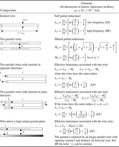
A collection of formulae for round wire structures such as pin connectors or vias in PCBs, is shown in Table A.1. It is worth making the following observations:
- Isolated wire. This is the situation that occurs when the current I on the conductor returns through another far away conductor and, therefore, the contribution of the mutual inductance can be neglected. The associated inductance is the self partial inductance Lp function of the length l and wire radius rw [1]. The low-frequency expression includes the internal wire inductance Lint = μ0/8π, and the resulting inductance is higher than the inductance at high frequency when the skin effect becomes dominant.
- Two parallel wires. The mutual partial inductance is calculated as mutual inductance between two filaments and provides exact values [1].
- Two parallel wires with currents in opposite directions. This is a favorable situation for the effective inductance associated with each conductor (i.e. signal and current return path), as the mutual partial inductance Mp must be algebraically subtracted from the self partial inductance Lp and the overall inductance of the two conductors is Let = 2(Lp − Mp).
- Two parallel wires with currents in the same direction. This is the case of a structure that consists of a return conductor far away from two parallel signal conductors where currents flow in the same direction. When the two currents are equal, the total effective inductance associated with the two conductors is Let = 1/2(Lp + Mp), which is lower than the self partial inductance of an isolated conductor Lp, as the mutual partial inductance between the two conductor Mp < Lp.
Table A.1 Inductance formulae for round-wire conductors
- Wire over a large return ground plane. For a wire above a ground plane with dimensions much larger than the height h, the method of image can be applied to calculate the effective inductance associated with the wire. The plane is replaced by a conductor parallel to the signal conductor, with equal current flowing in the opposite direction, and having a distance from the other twice the distance between the signal conductor and the ground plane. The result is the simple expression in Table A.1. This is also the overall inductance of the signal–ground loop, as the effective inductance associated with a large ground plane can be neglected (see the expression of the effective inductance Le gnd in Table A.2).
A.2 Busbars
A collection of formulae for busbar structures such as traces in PCBs, is shown in Table A.2. It is interesting to note the following:
- Isolated busbar. As in the case of round wire, this is the situation when the current I on the busbar, i.e. a PCB trace, returns through another conductor far away so that the contribution of the mutual inductance is negligible. The exact formula for the self partial inductance of a trace of width w, thickness t, and length l is reported elsewhere [2, 3]. As this expression is quite complicated, a simplified formula that works well for practical cases of interest is shown in Table A.2. For instance, it can be shown that, for 0 < t < 1 mm, w = 1 mm, and l ≥ w, the simple formula provides the same results as the exact formula.
- Two parallel busbars. In the case of parallel, rectangular cross-section conductors (bars), the exact expression of mutual partial inductance is again given elsewhere [2, 3]. If the bars are not too close, then a reasonable approximation is to treat them as filaments and use the formula of Table A.1. Another more accurate method is to divide the cross-section of each bar into sub-bars, treat each of them as a filament, then use the filament approximation of Table A.1 to characterize each sub-bar, and finally sum the results as indicated in Table A.2. It can be shown that the three methods give the same results for practical situations. For instance, for a parallel busbar with w = 0.25 mm and t = 0.1 mm, and assuming that Kx = Mx = 2 and Ky = My = 5, the results are practically coincident for d ≥ 0.25 mm in configuration (a) and for d ≥ 0.35 in configuration (b). For both cases, l ≥ 1 mm. In conclusion, the filament expression works as well as the expression with the summations for most cases of interest, except when the bar separation is of the order of the bar thickness.
- Parallel busbars with differential currents. The effective inductance to be associated with each conductor can be calculated as the difference between the self and mutual inductance by using the formulae given in Table A.2.
- A bar (trace) above a finite ground plane. This is a very important practical case because, once the effective inductance associated with the ground of a PCB is known, it is possible to calculate the radiated field from a PCB with an attached cable. Numerous examples are provided in Chapter 9. The formula given in Table A.2, taken from reference [4], works well, as demonstrated experimentally in Chapter 9. Other formulae can be found elsewhere [5, 6]. A general, accurate method, useful for various ground plane cross-sections, consists in computing the voltage drop along the ground plane that is caused by current I. The ground plane is divided into sub-bars, or filaments, and self and mutual partial inductances regarding all the conductors are accounted for. An example of application of this method for some structures of practical interest is outlined in Section 10.1.
- The onset frequency between the low- and high-frequency regions is the frequency where the skin effect becomes significant (see Section 7.1).
Table A.2 Inductance formulae for busbar conductors

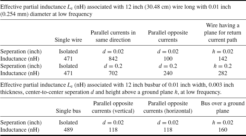
Table A.3 Table of sample inductance calculations
A.3 Examples of Application of the Inductance Formulae
An example of application of the inductance formulae is given in Table A.3. The numerical values refer to the effective inductance Le associated with each conductor when not isolated. The total inductance of the loop formed by the two conductors is 2Le when the conductors have equal and opposite currents and Le/2 when the conductors have equal current. Observe that, for conductors with opposite currents, the effective inductance Le = Lp − Mp decreases when the conductors are closer, as the self partial inductance Lp remains the same while the mutual partial inductance Mp increases. For conductors with currents in the same direction, to have a low value of Le = Lp + Mp, the mutual partial inductance Mp must be minimized by increasing the separation between the two conductors. On the other hand, to have high values of Le to stop the common-mode currents, Mp must be maximized by increasing the magnetic flux coupled between the two conductors, as done with choke EMI filters. In the case of two parallel busbars, the inductance does not change with the reciprocal position of the bars when the bars have the same center-to-center separation. For comparison purposes, the same structures were chosen as those considered in reference [7], where the dimensions are expressed in inches (1 inch = 2.54 cm).
References
[1] Grover, F.W., ‘Inductance Calculations’, Dover, New York, NY, 1946.
[2] Ruehli, A.E., ‘Inductance Calculations in a Complex Integrated Circuit Environment’, IBM Journal of Research and Development, 16, September 1972, 470–481.
[3] Hoer, C. and Love, C., ‘Exact Inductance Equations for Rectangular Conductors with Applications to More Complicated Geometries’, J. Research Natl. Bar. Stand. – C. Eng. Instrum., 69C, 1965, 127–137.
[4] Leferink, F., ‘Inductance Calculations: Methods and Equations’, IEEE International Symposium on Electromagnetic Compatibility, Atlanta, GA, 14–18 August 1995, 16–22.
[5] Hockanson, D., Drewniak, J., Hubing, T., Van Doren, T., Sha, F., Lam, C.-W., and Rubin, L., ‘Quantifying EMI Resulting from Finite-impedance Reference Planes’, IEEE Trans. on Electromagetic Compatibility, 39(4), November 1997, 286–297.
[6] Holloway, C. and Kuester, E., ‘Net and partial inductance of a microstrip ground plane’, IEEE Trans. on Electromagnetic Compatibility, 40(1), February 1998, 33–46.
[7] Rostek, P., ‘Avoid Wiring–Inductance Problems’, Electronic Design, 25, 6 December 1974.
Signal Integrity and Radiated Emission of High-Speed Digital Systems Spartaco Caniggia and Francescaromana Maradei
© 2008 John Wiley & Sons, Ltd