
Appendix B
Characteristic Impedance, Delay Time, and Attenuation of Microstrips and Striplines
This appendix provides closed-form expressions for calculating the characteristic impedance, delay time, and attenuation of traces having microstrip and stripline structures. A procedure for computing analytically the proximity-effect parameter Kp as defined in Chapter 7 is also outlined. Some results are compared with those found in the literature by using field-solver software.
B.1 Microstrip
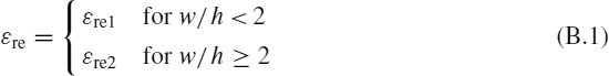
Microstrip has the structure shown in Figure B.1 and is characterized by fields propagating in two different dielectrics: air and substrate with relative permittivity εr. This is particularly true if the trace is not covered by a soldermask to prevent corrosion. Usually, an effective dielectric constant, εre, is used for electric parameter calculations, which is given by
where

The per-unit-length (p.u.l.) propagation delay time tpd is then given by
where μ0 = 4π × 10−7 H/m and ε0 = 8.854 × 10⁻¹² F/m.
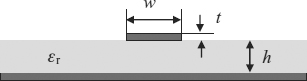
Figure B.1 Microstrip structure
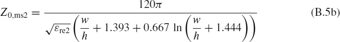
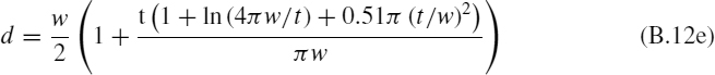
The microstrip characteristic impedance Z0,ms is given in closed form by [1]

where

The microstrip attenuation αt,ms can be calculated by the closed-form expression [1]
where αd,ms and αc,ms are the attenuation due to losses in dielectric and conductor media, respectively, considering the return path, also, as defined in Chapter 7. These parameters are given by


where tan δ is the dielectric loss tangent. The results of this calculation are in dB/inch, and the frequency must be assigned in GHz. The parameters w, t, and h must be set in mils. The proposed closed-form expressions give results in good agreement (less than 4 %) with those obtained by a field-solver code. Usually the trace has the structure of an embedded microstrip. The soldermask chemistry and final thickness is a 0.6–0.8 mil thick coating over the copper with εr = 3.1–3.3 and loss tangent tan δ ≈ 0.02. In this case there are three dielectrics involved, and the prediction of the effective dielectric permittivity εre and of the characteristic impedance Z0 change slightly. However, from an engineering viewpoint, the proposed formulation can still be used without losing significant accuracy, as will be demonstrated later with an example.
The accuracy of αd is better than 1%, and αc is suitable for w/h ranging between 0.159 and 2 or for microstrip on FR4 with Z0 from roughly 50 Ω and 100 Ω.
B.2 Stripline
Stripline is a conductor immersed in a dielectric and sandwiched between two return planes. The structure is symmetric when the trace is centered in the dielectric, as shown in Figure B.2, with h = b − t/2. An offset stripline is a structure with the trace closer to one plane. In contrast to microstrip, the field lines are confined into the dielectric, and therefore the p.u.l. propagation delay time depends on the relative permittivity εr and is given by
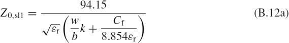
The stripline characteristic impedance Z0,sl can be calculated by the closed-form expressions [1]

where


The expressions for the case w/(b − t) ≥ 0.35 are valid for traces no thicker than 25% of the plate spacing. For a 1 oz trace, this means b ≥ 5.6 mils, which is generally met in practical PCB design. The trace thickness is rated in plating weight, typically reported in ounces. A 1 oz plating corresponds to a thickness of 34.8 μm. The thickness scales in proportion to plating weight [2].
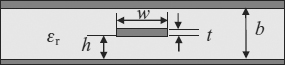
Figure B.2 Stripline structure
The proposed closed-form expressions provide results with discrepancies lower than 2% with respect to field-solver software solutions for a wide range of impedances and trace widths.
The stripline attenuation αt,sl can be calculated as the sum of attenuation due to dielectric αd,sl and conductor αc,sl by the following closed-form expression:
where


The results of this calculation are in dB/inch, and the frequency must be assigned in GHz. The parameters w, t, and b must be set in mils. The accuracy of αd is better than 1%. Considering αc, the expression should be valid only when w/(b − t) ≥ 0.35, i.e. for a wide trace having impedance below about 65 Ω. However, the expression provides acceptable accuracy for a higher-impedance trace.
B.3 Trace Attenuation and the Proximity-Effect Parameter
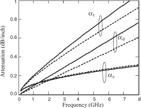
The closed-form expressions previously given were used to calculate the attenuation for stripline and microstrip traces with a characteristic impedance of 50 Ω, and the results are shown in Figure B.3. It can be noted that, above 1 GHz, the dielectric losses dominate, and this fact makes the accuracy of the formula used to calculate αc less important.
The proposed closed-form expressions can be very useful for calculating the proximity-effect parameter Kp as an alternative to field-solver software. The proximity factor takes into account the additional resistance due to redistribution of current on both the signal conductor and the reference planes, as defined in Section 7.1. The procedure consists of the following steps:
- The real part of the skin-effect impedance R0Skin at a particular frequency of interest f0 is calculated by combining Equations (7.5) and (7.19) and adopting a proximity factor Kp = 1:
where p = 2(t + w) is the perimeter of the trace, and σ is the conductivity of the trace.
Figure B.3 Attenuations in a 50 Ω stripline (solid line) and a 50 Ω microstrip (dashed line). Trace parameters: εr = 4.25, loss tangent tan δ = 0.02, w = 5 mils, t = 0.65 mils, b = 12.85 mils (stripline), h =3.0 mils (microstrip)
- The characteristic impedance Z0,i is calculated by Equation (B.4) with i = ‘ms’ for a microstrip or by Equation (B.11) with i = ‘sl’ for a stripline trace.
- The attenuation due to the skin effect only at frequency f0 and indicated here as α0Skin,i (with i = ‘ms’ or i = ‘sl’) is calculated in dB, considering that 1 neper = 8.686 dB and 1 inch = 0.0254 m (see Equations (7.32) and (7.39)). Therefore
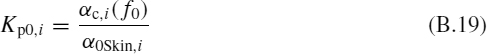
- The proximity factor Kp0,i at frequency f0 is computed as the ratio of the attenuation αc,i(f0) at frequency f0, computed by Equation (B.8) for i = ‘ms’ or by Equation (B.15) for i = ‘sl’, and the attenuation α0Skin,i for the skin effect only. Remember that Equations (B.8) and (B.15) take into account the skin effect and the proximity effect between the trace and its return path:
- The total resistance of the trace R0,i which incorporates the factor Kp0,i at frequency f0 is calculated as the product of the skin-effect resistance R0Skin and the proximity-effect parameter Kp0,i calculated by Equation (B.19):


To check the accuracy of this procedure, the values reported in Table 5.1 of reference [2] were used for comparison at a frequency f0 = 1 GHz and shown in round brackets in Table B.1. The resistance in [2] was calculated by a method-of-moments magnetic field simulator, and the authors estimate the accuracy of the data generated by this simulator at approximately ±2%.
Table B.1 Proximity-effect coefficient Kp0 and AC resistance R0 including Kp0 for single-ended microstrips and striplines computed for f0 = 1 GHz. The values in brackets come from Table 5.1 of reference [2]

The results of the proposed analytical procedure are summarized in Table B.1 for some trace structures. The data of Table 5.1, in brackets, are those reported in reference [2]. The comparison shows that there is a very good agreement, although the microstrips are with soldermask, and the analytical procedure of this appendix refers to bare microstrip structures. For the striplines there is a slight overestimation. Note that, at f = f0, the attenuation due to the dielectric αd(f0) is higher than the attenuation due to the conductor αc(f0) right from 1 GHz. This makes the inaccuracy introduced by the analytical calculation of the attenuation αc less critical. On the other hand, the attenuation αd has an accuracy lower than 1%.
References
[1] Thierauf, S.C., ‘High-speed Circuit Board Signal Integrity’, Artech House, Inc., Norwood, MA, 2004.
[2] Johnson, H. and Graham, M., ‘High-speed Signal Propagation: Advanced Black Magic’, Prentice Hall PTR, Upper Saddle River, NJ, 2003.
Signal Integrity and Radiated Emission of High-Speed Digital Systems Spartaco Caniggia and Francescaromana Maradei
© 2008 John Wiley & Sons, Ltd