
4
Capacitance
Capacitance is another very important line, filtering, and IC device parameter for Signal Integrity (SI) and Radiated Emission (RE). In this chapter, self and mutual capacitances are theoretically introduced, considering the coupling between two generic conductors. The capacitance C matrix concept for two coupled wires having a reference return conductor is introduced as background to build a C matrix for n-multiconductor transmission lines. Calculation of the inductance L matrix for multiconductor lines, starting with the C matrix, is considered. Finally, the definitions of Differential Mode (DM) and Common Mode (CM) capacitances are given.
4.1 Capacitance Between Conductors
The capacitance is a very important parameter in modeling interconnects. Starting with the basic definition of capacitance, the concept is then extended to a general multiconductor formulation which is essential, as many interconnects consist of several coupled lines. Particular emphasis is given to the capacitance C matrix and its negative off-diagonal terms, as this concept is fundamental to understanding the output of a static field solver for building transmission-line models.
4.1.1 Definition of Capacitance
Capacitance is a property of a geometric configuration defined by two conducting objects surrounded by a homogeneous dielectric. It describes the ability of the given configuration to store electrostatic energy [1–3]. Consider, for example, the geometry shown in Figure 4.1, where two conductors charged with a total charge Q of opposite sign are surrounded by a homogeneous dielectric medium of dielectric constant ε = ε0εr, where ε0 = 8.854 × 10⁻¹² F/m is the vacuum permittivity and εr is the relative permittivity. As a result of this charge distribution, there is an electric flux emanating from the positive charge and terminating at the negative one. Gauss' law relates the electric field ![]() or the electric flux density
or the electric flux density ![]() to the charge Q according to
to the charge Q according to

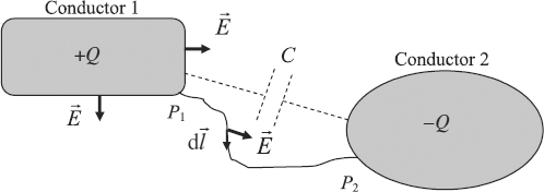
Figure 4.1 Capacitance between two conductors
where ρ is the charge density in the volume V, and S is a closed surface around conductor 1 only. Gauss' law (4.1) simply indicates that the total electric flux density emanating from the closed surface S is equal to the total charge enclosed by the surface. Equation (4.1) exhibits a linear charge–electric field relation; this means that a doubling of Q is accompanied with a doubling of E. The voltage between the two conductors is defined by

where ![]() is the unit vector tangent to any line between points P1 and P2. A linear relation can be observed in Equation (4.2) between the voltage V and the electric field. Therefore, the voltage is linearly dependent on the total charge by a coefficient c called the capacitance. The capacitance of this two-conductor system is defined as the ratio of the positive charge Q to the resulting potential difference V between the two conductors:
is the unit vector tangent to any line between points P1 and P2. A linear relation can be observed in Equation (4.2) between the voltage V and the electric field. Therefore, the voltage is linearly dependent on the total charge by a coefficient c called the capacitance. The capacitance of this two-conductor system is defined as the ratio of the positive charge Q to the resulting potential difference V between the two conductors:
Hence, the capacitance is independent of the specific amount of charge on the conductors and of the specific value of the potential difference between them.
The current I flowing through the capacitance c in the time domain is given by
For a given geometry of the two-conductor system, there are two procedures for calculating c. In the first one, a charge Q of opposite sign is assigned to the conductors, and the resulting electric field is calculated by Gauss' law or by other means. Then the potential difference between the two conductors is found by Equation 4.2, and the capacitance is obtained through Equation (4.3). In the second procedure, a potential difference between the two conductors is assigned, and the total charge on the conductors is calculated. This latter procedure requires the solution of the Laplace equation.
4.1.2 Partial Capacitance and Capacitance Matrix of Two Coupled Conductors Having a Reference Return Conductor
Capacitance is present between any two charged metallic surfaces at different potentials. When more than two conductors are present, Equation (4.3) can be repeatedly applied to obtain the partial capacitances between each couple of conductors of the whole group.
Consider, for simplicity, the three-wire configuration shown in Figure 4.2a, where conductor 0 is assumed to be grounded (i.e. V0 = 0) and represents the reference conductor. In practical applications, the reference conductor is often given by a ground plane. The wires are assumed to be electrically short and charged with Q0, Q1, and Q2 respectively. The potential difference between the conductors and the grounded reference are indicated as V1 and V2. In the considered configuration of Figure 4.2a, c10 and c20 represent the capacitive coupling between conductors 1 and 2 and the reference, while the mutual capacitance c12 expresses the capacitive coupling between conductor 1 and conductor 2.
The voltage V1 between conductors 1 and 0 is supported by a charge Q10 = c10V1 on conductor 1 and by −Q10 on conductor 0. Analogously, the voltage (V1 − V2) between conductors 1 and 2 is supported by a charge Q12 = c12(V 1 − V 2) on conductor 1 and by −Q12 on conductor 2. The total charge on conductor 1 is the sum of these two charges Q1 = Q10 + Q12.
The wire currents I1 and I2 shown in Figure 4.2b as functions of voltages and capacitances can then be expressed as
or in matrix form as
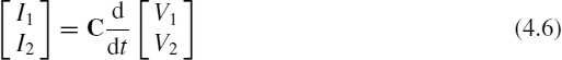

Figure 4.2 Capacitances between two conductors and their reference: (a) transversal representation; (b) longitudinal representation
where C is the capacitance matrix given by

The diagonal terms in matrix (4.7) are the self capacitances and represent the displacement currents flowing from a given conductor to ground when the other conductor is grounded. It should be noted that the self capacitance is not the wire-to-ground capacitance. The off-diagonal terms in matrix (4.7) are always negative and are the mutual capacitances with changed sign.
4.1.3 Capacitance Matrix of n Coupled Conductors Having a Reference Return Conductor
The capacitance matrix C introduced in the previous section for the two-conductor configuration can be easily extended to the more general configuration of n coupled lines having a reference return conductor [4]. In this case, the diagonal and off-diagonal terms are given by
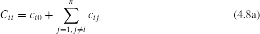
The diagonal term Cii in Equation (4.8a) is given by the sum of the ith wire-to-ground capacitance ci0 and the mutual capacitances cij between the ith and the other wires. The off-diagonal term Cij in Equation (4.8b) is always negative and is given by the mutual capacitance between the ith and jth conductors with changed sign. It is important to point out that the coefficients of the capacitance matrix (4.7) have no physical meaning, but they can be used to calculate the physical partial capacitances between conductors.
Because of the reciprocity of capacitance, capacitance matrices are also reciprocal, so Cij = Cji, and the matrix is symmetric.
If the medium surrounding the conductors is homogeneous and characterized by permittivity εr and relative permeability μr, the following relationship between capacitance and inductance matrices holds:
where I is the n × n identity matrix. Therefore, only one of the parameter matrices needs to be calculated. In general, the static field solvers firstly calculate the matrix C while deriving the matrix L by Equation (4.9).
Usually, in practical configurations, the medium surrounding the conductors is characterized by an inhomogeneous dielectric constant and permeability μr = 1. As the inductance matrix is not affected by the dielectric inhomogeneity, it can be derived from the knowledge of the capacitance matrix C0 obtained by replacing the dielectric with free space. Thus, for inhomogeneous media, the computation of the capacitance matrix is performed twice, with and without the presence of the dielectric.
4.2 Differential Mode and Common Mode Capacitance
In high-speed digital systems the concept of differential mode (DM) and common mode (CM) capacitance is very useful for crosstalk modeling, for differential signaling investigation, and for choosing the appropriate filters to mitigate conducted and radiated emission. The effective capacitance associated with each conductor for differential mode and common mode will be used in Section 6.2 to introduce a transmission-line model for two symmetric lines based on two decoupled modes of propagation (i.e. even and odd modes) characterized by proper characteristic impedance and delay. It will be shown that even and odd modes are directly related to differential mode and common mode.
4.2.1 Differential Mode Capacitance
When, in the configuration of Figure 4.2, the two voltages V1 and V2 are forced to be equal in magnitude and opposite in sign (see Figure 4.3), Equations (4.5) become
where ce1 and ce2 are the effective capacitances associated with the two conductors, given by
Based on Equation (4.10), the differential mode circuit shown on the righthand side of Figure 4.3 is obtained, and the differential mode capacitance between conductor 1 and conductor 2 is given by
If the structure is symmetric, then c10 = c20 = c0. In this case, the two effective capacitances are equal to ce1 = ce2 = ceDM = c0 + 2cm, with c12 = cm, and the differential mode capacitance CDM and the effective differential mode capacitance CeDM are given by
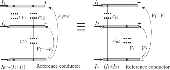
Figure 4.3 Equivalent circuits for differential mode capacitance
Equation (4.12a) provides the true differential mode capacitance between the two conductors. Equation (4.12b) will be used in Section 6.2 to calculate the transmission-line parameters associated with the odd mode.
4.2.2 Common Mode Capacitance
When the two voltages V1 and V2 are forced to be equal in magnitude, the mutual capacitance c12 is not involved by any current circulation (see Figure 4.4). In this case, equations (4.5) can be rewritten as
where
Based on Equations (4.13), the common mode circuit shown on the right-side of Figure 4.4 is obtained. The common mode capacitance between conductors 1 and 2, which are in parallel, and the reference conductor is then defined as
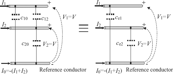
Figure 4.4 Equivalent circuits for common mode capacitance
If the structure is symmetric, then c10 = c20 = c0 and the common mode capacitance is
This means that the common mode capacitance coincides with the even-mode capacitance as defined in Section 6.2. Equation (4.16) will be used to calculate the line parameters associated with the even mode.
References
[1] Ramo, S., Whinnery, J., and Van Duzer, T., ‘Fields and Waves in Communication Electronics’, 3rd edition, John Wiley & Sons, Inc., New York, NY, 1994.
[2] Young, B., ‘Digital Signal Integrity: Modeling and Simulation with Interconnects and Packages’, Prentice Hall PTR, Upper Saddle River, NJ, 2001.
[3] Paul, C., ‘Introduction to Electromagnetic Compatibility’, John Wiley & Sons, Inc., Hoboken, NJ, 2006.
[4] Paul, C., ‘Analysis of Multiconductor Transmission Lines’, John Wiley & Sons, Inc., New York, NY, 1994.
Signal Integrity and Radiated Emission of High-Speed Digital Systems Spartaco Caniggia and Francescaromana Maradei
© 2008 John Wiley & Sons, Ltd