
Memory System Design Analysis
In recent years, the importance of memory system performance as a limiter of computer system performance has been widely recognized. However, the commodity nature of mainstream DRAM devices means that DRAM design engineers are reluctant to add functionalities or to restructure DRAM devices that would increase the manufacturing cost of those devices. The direct consequence of the constraints on available features of commodity DRAM devices is that system architects and design engineers must carefully examine the system-level, multi-variable equations that trade off cost against performance, power consumption, reliability, user configuration flexibility, and a myriad of other design considerations. Consequently, the topic of memory system performance analysis is important not only to system architects, but also to DRAM system and device design engineers to evaluate design trade-off points between the cost and benefits of various features.
This chapter examines performance issues and proceeds along a generalized framework to examine memory system performance characteristics. The goal of the illustrative examples contained in this chapter is not to answer every and all design questions that a memory system architect may have in the evaluation of his or her memory system architecture. Rather, the goal of this chapter is to provide illustrative examples that a potential system architect can follow and gain potential insight into how his or her memory system should or could be analyzed.
15.1 Overview
Figure 15.1 shows the scaling trends of commodity DRAM devices. The figure shows that in the time period shown, from 1998 to 2006, random row cycle times in commodity DRAM devices decreased on the order of 7% per year, and the data rate of commodity DRAM devices doubled every three years. The general trend illustrated in Figure 15.1 means that it is more difficult to sustain peak bandwidth from successive generations of commodity DRAM devices, and the topic of memory system performance analysis becomes more important with each passing year. Consequently, the topic of memory system design and performance analysis is similarly gaining more interest from industry and academia with each passing year. However, the topic of memory system design and performance analysis is an extremely complex topic; a system-specific, optimal memory system design depends on system-specfic workload characteristics, cost constraints, bandwidth versus latency performance requirements, and power design envelope, as well as reliability considerations. That is, there is no single memory system that is near-optimal for all workloads. The topic is of sufficient complexity that a single chapter designed to outline the basic issues cannot provide complete coverage in terms of width and depth. Rather, the limited scope of this chapter is to provide an overview and some illustrative examples of how memory system performance analysis can be performed.

The logical first step in the design process of a memory system is to define the constraints that are important to the system architect and design engineers. Typically, a given memory system may be cost constrained, power constrained, performance constrained, or a reasonable combination thereof. In the case where one constraint predominates the design consideration process, the system architect and engineer may have little choice but to pursue design points that optimize for the singular, overriding constraint. However, in the cases where the design process has multi-dimensional flexibility in trading off cost against performance, the second step that should be taken in the design process of the memory system is to explore the workload characteristics that the memory system is designed to handle. That is, without an understanding of the workload characteristics that the memory system should be optimized for, the mismatch in respective points of optimality can lead to a situation where the system may be overdesigned for workload characteristics that seldom occur and at the same time poorly designed to handle more common workload characteristics.
This chapter on the performance and design analysis of memory system performance characteristics begins with a section that examines several single threaded workloads commonly used for benchmarking purposes. The section on workload characteristics examines the various single threaded workloads in terms of their respective request inter-arrival rate, locality characteristics, and read-versus-write traffic ratio. The rationale for the examination of the workload characteristics is to provide a basis for understanding different types of workload characteristics. However, one caveat that should be observed is that the workloads examined in Section 15.2 are somewhat typical workloads for uniprocessor desktop and workstation class computer systems. More modern memory systems designed for multi-threaded and multi-core processors must be designed to handle complex multi-threaded and multiple concurrent process workloads. Consequently, the workloads examined in Section 15.2 are not broadly applicable to this class of systems. In particular, systems designed for highly threaded, on-line transaction processing (OLTP) types of applications will have drastically different memory system requirements than systems designed for bandwidth-intensive scientific workloads. Nevertheless, Section 15.2 can provide the reader with a baseline understanding of issues that are important in the design and analysis of a memory system.
The remainder of the chapter following the workload description section can be broadly divided into two sections that use slightly varying techniques to analyze a similar set of issues. In Section 15.3 the Request Access Distance (RAD) analytical framework provides a set of mathematical equations to analyze sustainable bandwidth characteristics, given specific memory-access patterns and scheduling policies from the memory controller. The RAD analytical framework is then used to examine a variety of issues relating to system-level parallelism and bandwidth characteristics. Finally, to complement the equation-based RAD analytical framework for DRAM memory system bandwidth analysis, Sections 15.4 and 15.5 use the more traditional approach of a memory system simulator to separately examine the issue of controller scheduling policy, controller queue depth, burst length, memory device improvements, and latency distribution characteristics.
15.2 Workload Characteristics
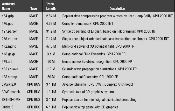
The performance characteristics of any given DRAM memory system depend on workload-specific characteristics of access rates and access patterns. In essence, one of the first steps in the design process of a memory system should be an examination of workloads that the memory system is to be optimized for. To facilitate a general understanding of workload behavior, and to examine a range of workload-specific variances, a large set of memory address traces from different applications is examined in this section and is summarized in Table 15.1. From the SPEC CPU 2000 benchmark suite, address traces from 164.gzip, 176.gcc, 197.parser, 255.vortex, 172.mgrid, 178.galgel, 179.art, 183.equake, and 188.ammp are used. The address traces from the SPEC CPU 2000 benchmark suite were captured with the MASE simulation framework through the simulated execution of 2 to 4 billion instructions, and the number of requests in each address trace is reported as trace length in Table 15.1 [Larson 2001]. In addition to the address traces captured with MASE, processor bus traces captured with a digital logic analyzer from a personal computer system running various benchmarks and applications such as JMark 2.0, 3DWinbench, SETI@HOME, and Quake 3 are added to the mix. Collectively, the SPEC CPU 2000 workload traces and desktop computer application traces form a diverse set of workloads that are described herein. In the following subsections, the characteristics for a small subsection of each workload are represented graphically. The various diagrams graphically illustrate the request inter-arrival rates and the respective read-versus-write ratios within short periods of time. The diagrams are captured from a bus trace viewer written specifically for the purpose of demonstrating the bursty nature of memory-access patterns.
15.2.1 164.gzip: C Compression
164.gzip is a popular data compression program written by Jean-Loup Gailly for the GNU project, and it is included as part of the SPEC CPU 2000 integer benchmark suite. 164.gzip uses Lempel-Ziv coding (LZ77) as its compression algorithm. In the captured trace for 164.gzip, 4 billion simulated instructions were executed by the simulator over 2 billion simulated processor cycles, and 2.87 million memory requests were captured in the trace. Figure 15.2 shows the memory traffic of 164.gzip for the first 4 billion simulated instructions in terms of the number of memory transactions per unit time. Each pixel on the x-axis in Figure 15.2 represents 2.5 million simulated processor cycles, and Figure 15.2 shows that 164 gzip typically averages less than 5000 transactions per 2.5 million microprocessor cycles, but for short periods of time, write bursts can average nearly 10,000 cacheline transaction requests per 2.5 million simulated processor cycles.1 Figure 15.2 shows that in the first 1.75 billion processor cycles, 164.gzip undergoes a short duration of program initialization and then quickly enters into a series of repetitive loops. Figure 15.2 also shows that 164.gzip is typically not memory intensive, and the trace averages less than 1 memory reference per 1000 instructions for the time period shown.

15.2.2 176.gcc: C Programming Language Compiler
176.gcc is a benchmark in the SPEC CPU 2000 integer benchmark suite that tests compiler performance. In the captured trace for 176.gcc, 1.5 billion instructions were executed by the simulator over 1.63 billion simulated processor cycles, and 4.62 million memory requests were captured in the trace during this simulated execution of the 176.gcc benchmark. Unlike 164.gzip, 176.gcc does not enter into a discernible and repetitive loop behavior within the first 1.5 billion instructions. Figure 15.3 shows the memory system activity of 176.gcc through the first 1.4 billion processor cycles, and it shows that 176.gcc, like 164.gzip, is typically not memory intensive, although it does averages more than 3 memory references per 1000 instructions. Moreover, in the time-frame illustrated in Figure 15.3, 176.gcc shows a heavy component of memory access due to instruction-fetch requests and relatively fewer memory write requests. The reason that the trace in Figure 15.3 shows a high percentage of instruction-fetch requests may be due to the fact that the trace was captured with the L2 cache of the simulated processor set to 256 kB in size. Presumably, a processor with a larger cache may be able to reduce its bandwidth demand on the memory system, depending on the locality characteristics of the specific workload.

15.2.3 197.parser: C Word Processing
197.parser is a benchmark in the SPEC CPU 2000 integer suite that performs syntactic parsing of English based on link grammar. In the captured trace for 197.parser, 4 billion instructions were executed by the simulator over 6.7 billion simulated processor cycles, and 31.2 million cacheline requests to memory were captured in the memory-access trace. Similar to 164 gzip, 197.gzip undergoes a short duration of program initialization and then quickly enters into a repetitive loop. However, 197.gzip enters into loops that are relatively short in duration and are difficult to observe in an overview. The close-up view provided in Figure 15.4 shows that each loop lasts for approximately 6 million microprocessor cycles, and the number of reads and write requests is roughly equal. Overall, Figure 15.4 shows the memory system activity of 197.parser through the first 6.7 billion processor cycles, and it shows that 197.parser is moderately memory intensive, averaging approximately 8 cacheline transaction requests per 1000 instructions.

15.2.4 255.vortex: C Object-Oriented Database
255.vortex is a benchmark in the SPEC CPU 2000 integer suite. In the captured trace for 255.vortex, 4 billion simulated instructions were executed by the simulator over 3.3 billion simulated processor cycles, and 7.2 million cacheline transaction requests to memory were captured in the trace. In the first 3.3 billion processor cycles, 255.vortex goes through several distinct patterns of behavior. However, after a 1.5-billion-cycle initialization phase, 255.vortext appears to settle into execution loops that last for 700 million processor cycles each, and each loop appears to be dominated by instruction-fetch and memory read requests with relatively fewer memory write requests. Figure 15.5 shows the memory system activity of 255.vortex through the first 3.3 billion processor cycles. Figure 15.5 also shows that 255.vortex is typically not memory intensive, since it averages less than 2 memory transaction requests per 1000 instructions.

15.2.5 172.mgrid: Fortran 77 Multi-Grid Solver: 3D Potential Field
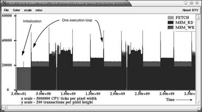
172.mgrid is a benchmark that demonstrates the capabilities of a very simple multi-grid solver in computing a three-dimensional (3D) potential field. It was adapted by SPEC from the NAS Parallel Benchmarks with modifications for portability and a different workload. In the captured trace for 172. mgrid, 4 billion simulated instructions were executed by the simulator over 9 billion simulated processor cycles, and 47.5 million requests were captured in the trace. 172.mgrid is moderately memory intensive, as it generates nearly 12 memory requests per 1000 instructions. Figure 15.6 shows that after a short initialization period, 172.mgrid settles into a repetitive and predictable loop behavior. The loops are dominated by memory read transaction requests, and memory write transaction requests are relatively fewer.
15.2.6 SETI@HOME
Distinctly separate from the SPEC CPU benchmark traces captured through the use of a simulator, a different set of application traces was captured through the use of a logic analyzer. The SETI@HOME application trace is one of four processor bus activity traces in Table 15.1 that was captured through the use of a logic analyzer. SETI@HOME is a popular program that allows the SETI (Search for Extra Terrestrial Intelligence) Institute to make use of spare processing power on idle personal computers to search for signs of extraterrestrial intelligence. The SETI@HOME application performs a series of fast Fourier transforms (FFTs) on captured electronic signals to look for the existence of signal patterns that may be indicative of an attempt by extraterrestrial intelligence to communicate. The series of FFTs are performed on successively larger portions of the signal file. As a result, the size of the working set for the program changes as it proceeds through execution. Figure 15.7 shows a portion of the SETI@HOME workload. In this segment, the memory request rate is approximately 12∼14 transactions per microsecond, and the workload alternates between read-to-write transaction ratios of 1:1 and 2:1. Finally, the effects of the disruption caused by the system context switch can be seen once every 10 ms in Figure 15.7.

FIGURE 15.7 Portions of SETI@HOME workload.
15.2.7 Quake 3
Quake 3 is a popular game for the personal computer, and Figure 15.8 shows a short segment of the Quake 3 processor bus trace, randomly captured as the Quake 3 game runs in a demonstration mode on a personal computer system. Figure 15.8 shows that the processor bus activity of the game is very bursty. However, a cyclic behavior appears in the trace with a frequency of approximately once every 70 ms. Interestingly, the frequency of the cyclic behavior coincides with the frame rate of the Quake 3 game on the host system.

15.2.8 178.galgel, 179.art, 183.equake, 188. ammp, JMark 2.0, and 3DWinbench
In the following sections, memory-access characteristics for several workloads are described, but not separately illustrated. The workloads listed in Table 15.1, but not separately illustrated, are 178.galgel, 179.art, 183.equake,188.ammp, JMark 2.0, and 3DWinbench.
In the captured trace for 178.galgel, 4 billion simulated instructions were executed by the simulator over 2.2 billion simulated processor cycles, and 3.1 million requests were captured in the trace. Relative to the other workloads listed in Table 15.1, 178 galgel is not memory intensive, and it generates less than 1 memory request per 1000 instructions. In the captured trace, 178.galgel settles into a repetitive and predictable loop behavior after a short initialization period.
179.art is a benchmark derived from an application that emulates a neural network and attempts to recognize objects in a thermal image. In the captured trace for 179.art, 450 million simulated instructions were executed by the simulator over 14.2 billion simulated processor cycles, and 90 million requests were captured in the trace. 179.art is extremely memory intensive, and it generates nearly 200 memory transaction requests per 1000 instructions. In the captured trace for 179.art, more than 95% of the memory traffic are memory read transactions.
In the captured trace for 183.quake, 1.4 billion simulated instructions were executed by the simulator over 1.8 billion simulated processor cycles, and 7.9 million requests were captured in the trace. In the captured trace, after an initialization period, 183.equake settles into a repetitive and predictable loop behavior. The loops are dominated by memory read requests, and memory write requests are relatively fewer outside of the initialization phase. 183.equake is moderately memory intensive, and it generates almost 6 memory references per 1000 instructions.
For the 188.ammp benchmark, 4 billion simulated instructions were executed by the simulator over 10.5 billion simulated processor cycles, and 60 million requests were captured in the trace. Table 15.1 shows that 188.ammp is moderately memory intensive. It generates approximately 15 memory references per 1000 instructions.
Differing from the SPEC CPU workloads, 3DWinbench is a suite of benchmarks that is designed to test the 3D graphics capability of a system, and the trace for this workload was captured by using a logic analyzer that monitors activity on the processor bus of the system under test. The CPU component of the 3DWinbench benchmark suite tests the processor capability, and the trace shows a moderate amount of memory traffic. 3DWinbench achieves a sustained peak rate of approximately 5 transactions per microsecond during short bursts, and it sustains at least 1 transaction per microsecond throughout the trace.
Finally, for the JMark 2.0 CPU, AWT and Complex Mathematics benchmarks from the JMark 2.0 suite are independent benchmarks in this suite of benchmarks. Compared to other workloads examined in this work, the benchmarks in JMark 2.0 access memory only very infrequently. Ordinarily, the relatively low access rate of these benchmarks would exclude them as workloads of importance in a study of memory system performance characteristics. However, the benchmarks in JMark 2.0 exhibit an interesting behavior in access memory in that they repeatedly access memory with locked reads and locked write requests at the exact same location. As a result, these application traces are included for completeness to illustrate a type of workload that performs poorly in DRAM memory systems regardless of system configuration.
15.2.9 Summary of Workload Characteristics
Figures 15.2-15.8 graphically illustrate workload characteristics of selected benchmarks listed in Table 15.1. Collectively, Figures 15.2-15.8 show that while the memory-access traces for some workloads exhibited regular, cyclic behavior as the workloads proceeded through execution, other workloads exhibited memory-access patterns that are non-cyclic and non-predictive in nature. Consequently, Figures 15.2-15.8 show that it is difficult to design a memory system that can provide optimal performance for all applications irrespective of their memory-access characteristics, but it is easier to design optimal memory systems in the case where the workload and the predominant memoryaccess patterns are known a priori. For example, low-latency memory systems designed for network packet switching applications and high-bandwidth memory systems designed for graphics processors can respectively focus on and optimize for the predominant access patterns in each case, whereas the memory controller for a multi-core processor may have to separately support single threaded, latency-critical applications as well as multi-threaded, bandwidth-critical applications.
Aside from illustrating the bursty and possibly non-predictive nature of memory-access patterns in general, Figures 15.2-15.8 also illustrate that for most workloads, the ratio of read and instruction-fetch requests versus write requests far exceeds 1:1. In combination with the observation that write requests are typically not performance critical, Figures 15.2-15.8 serve as graphical justification. For memory systems that design in asymmetrical bandwidth capabilities as part of the architectural specification. For example, the FB-DIMM memory system and IBM’s POWER4 and POWER5 memory systems all respectively design in a 2:1 ratio in read-to-write bandwidth.
15.3 The RAD Analytical Framework
The RAD analytical framework computes the maximum sustainable bandwidth of a DRAM memory system by meticulously accounting for the various overheads in the DRAM memory-access protocol. In the RAD analytical framework, DRAM refresh is considered as a fixed overhead, and its effects are not accounted for in the framework, but must be accounted for separately. Aside from the effects of DRAM refresh, the methodology to account for the primary causes of bandwidth inefficiency in DRAM memory systems is described in detail in the following sections.
The RAD analytical framework formalizes the methodology for the computation of maximum sustainable DRAM memory system bandwidth, subjected to different configurations, timing parameters, and memory-access patterns. However, the use of the RAD analytical framework does not reduce the complexity of analysis nor does it reduce the number of independent variables that collectively impact the performance of a DRAM memory system. The RAD analytical framework simply identifies the factors that limit DRAM bandwidth efficiency and formalizes the methodology that computes their interrelated contributions that collectively limit DRAM memory system bandwidth.
The basic idea of the RAD analytical framework is simply to compute the number of cycles that a given DRAM memory system spends in actively transporting data, as compared to the number of cycles that must be wasted due to various overheads. The maximum efficiency of the DRAM memory system can then be simply computed as in Equation 15.1.
15.3.1 DRAM-Access Protocol
The basic DRAM memory-access protocol and the respective inter-command constraints are examined in a separate chapter and will not be repeated here. Rather, the analysis in this chapter simply assumes that the interrelated constraints between DRAM commands in terms of timing parameters are understood by the reader. Nevertheless, the basic timing parameters used in the basic DRAMaccess protocol are summarized in Table 15.2. These timing parameters are used throughout the remainder of this chapter to facilitate in the analysis of the memory system.
TABLE 15.2
Summary of timing parameters used in the generic DRAM-access protocol
| Parameter | Description |
| tAL | Added Latency to column accesses, used in DDRx SDRAM devices for posted CAS commands. |
| tBURST | Data burst duration. The number of cycles that data burst occupies on the data bus. In DDR SDRAM, 4 beats occupy 2 clock cycles. |
| tCAS | Column Access Strobe latency. The time interval between column access command and the start of data return by the DRAM device(s). |
| tCCD | Column-to-Column Delay. Minimum intra-device column-to-column command timing, determined by internal burst (prefetch) length. |
| tCMD | Command transport duration. The time period that a command occupies on the command bus. |
| tCWD | Column Write Delay. The time interval between issuance of a column write command and placement of data on data bus by the controller. |
| tFAW | Four (row) bank Activation Window. A rolling time-frame in which a maximum of four bank activations can be initiated. |
| tOST | ODT Switching Time. The time interval to switching ODT control from rank to rank. |
| tRAS | Row Access Strobe. The time interval between row access command and data restoration in a DRAM array. |
| tRC | Row Cycle. The time interval between accesses to different rows in a bank. tRC = tRAS + tRP. |
| tRCD | Row to Column command Delay. The time interval between row access and data ready at sense amplifiers. |
| tRFC | Refresh Cycle Time. The time interval between refresh and activation commands. |
| tRP | Row Precharge. The time interval that it takes for a DRAM array to be precharged for another row access. |
| tRRD | Row activation to Row activation Delay. The minimum time interval between two row activation commands to the same DRAM device. |
| tRTP | Read to Precharge. The time interval between a read and a precharge command. Can be approximated by tCAS – tCMD. |
| tRTRS | Rank-to-rank switching time. Used in DDR and DDR2 SDRAM memory systems. |
| tWR | Write Recovery time. The minimum time interval between the end of write data burst and the start of a precharge command. |
| tWTR | Write To Read delay time. The minimum time interval between the end of write data burst and the start of a column read command. |
15.3.2 Computing DRAM Protocol Overheads
In the RAD analytical framework, the limiters of DRAM memory system bandwidth are separated into three general catagories: inter-command constraints, row cycle constraints, and per-rank, row activation constraints. These respective categories are examined separately, but ultimately are combined into a single set of equations that form the foundation of the RAD analytical framework.
The first category of constraints that limit DRAM memory system bandwidth consists of inter-command constraints. Inter-command constraints are simply the inability to issue consecutive column access commands to move data in the DRAM memory system. For example, read-write turnaround overhead on the data bus or rank-to-rank switching times are both examples of inter-command constraints. Collectively, these inter-command constraints are referred to as DRAM protocol overheads in the RAD analytical framework. Table 15.3 summarizes the DRAM protocol overheads for consecutive column access commands. Table 15.3 lists the DRAM protocol overheads in terms of gaps between data bursts on the data bus, and that gap is reported in units of tBURST. In the RAD analytical framework, the DRAM protocol overhead between a request (column access command) j and the request that immediately precedes it, request j – 1, is denoted by Do(j), and Do(j) can be computed by using request j and request j – 1 as indices into Table 15.3.

15.3.3 Computing Row Cycle Time Constraints
The second category of command constraints that limit DRAM memory system bandwidth consists of DRAM bank row cycle time constraints. In the RAD analytical framework, the minimum access distance Dm is defined as the number of requests (column access commands) that must be made to an open row of a given bank or to different banks, between two requests to the same bank that require a row cycle for that bank. In the RAD analytical framework, the basic unit for the minimum access distance statistic is the data bus utilization time for a single transaction request, tBURST time period, and each request has a distance value of 1 by definition. In a close-page memory system with row cycle time of tRC and access burst duration of tBURST, Dm is simply (tRC − tBURST) /tBURST.
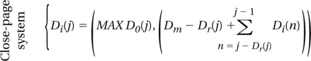
In the RAD analytical framework, a request j is defined to have a request access distance Dr(j) to a prior request made to a different row of the same bank as request j. The request access distance Dr(j) denotes the timing distance between it and the previous request to a different row of the same bank. In the case where two requests are made to different rows of the same bank and where there are fewer than Dm requests made to the same open bank or different banks, some idle time must be inserted into the command and data busses of the DRAM memory system. Conseqeuntly, if Dr(j) is less than Dm, some amount of idle time, Di(j), must be added so that the total access distance for request j, Dr(j) + Di(j), is greater than or equal to Dm. The definition for the various distances, Dm, Dr(j), and Di(j), holds true for close-page memory systems as defined.
The key element in the RAD analytical framework for the computation of DRAM memory system bandwidth efficiency is the set of formulas used to compute the necessary idling distances for each request in a request stream. The fundamental insight that enables the creation of the request access distance statistic is that idling distances added for Dr(j) requests immediately preceding request j must be counted toward the total access distance needed by request j since these idling distances increase the effective access distance of request j. The formula for computing the additional idling distances needed by request j for close-page memory systems is illustrated as Equation 15.2.
(EQ 15.2)
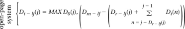
However, due to the differences in row buffer management, different request distances and equations are needed for open-page memory systems separate from close-page memory systems. In an open-page memory system, a row is kept active at the sense amplifiers once it is activated so that subsequent column accesses to the same row can be issued without additional row cycles. In the case of a bank conflict in an open-page memory system between two requests to different rows of the same bank, the second request may not need to wait the entire row cycle time before it can be issued. Figure 15.9 shows that in the best case, bank conflicts between two different column access requests can be scheduled with the timing of tBURST + tRP + tRCD if the row restoration time tRAS has already been satisfied for the previous row access. In the best-case scenario, the minimum scheduling distance between two column commands in an open-page system to different rows of the same bank is (tRP + tRCD) / tBURST. The best-case scenario illustrated in Figure 15.9 shows that Dm is by itself insufficient to describe the required minimum access distance in an open-page system. Consequently, two different minimum request access distances, Dm-ff and Dm-lf, are separately defined for open-page memory systems to represent the worst-case and best-case timing between column accesses to different rows of the same bank in the RAD framework, respectively. The variable Dm-ff denotes the minimum request access distance between the first column access of a row access and the first column access to the previously accessed row of the same bank. The variable Dm-lf denotes the first column access of a row access and the last column access to the previously accessed row of the same bank. In the same manner that request access distance for request j, Dr(j), is defined to compute the number of additional idle distances that is needed to satisfy Dm for close-page memory systems, two different request distances, Dr-ff(j) and Dr-lf(j), are defined in open-page memory systems to compute the additional idling distances needed to satisfy Dm-ff and Dm-lf, respectively.

In the computation for additional idling distances, Dr-ff(j) and Dr-lf(j) are needed for request j if and only if request j is the first column access of a given row access. If request j is not the first column access of a row access to a given bank, then the respective row activation and precharge time constraints do not apply, and Dr-ff(j) and Dr-lf(j) are not needed.
In cases where either Dr-ff(j) is less than Dm-ff or Dr-lf(j) is less than Dm-lf, additional idling distances must be added. In an open-page memory system, Di(j) is equal to the larger value of Di-ff(j) and Di-lf(j) for request j that is the first column access of a given row. In the case that a given request j is not the first column access of a given row, Di(j) is zero. The equations for the computation of idling distances Di-ff(j) and Di-lf(j) are illustrated as Equations 15.3 and 15.4, respectively. Finally, the various request access distance definitions for both open-page and close-page memory systems are summarized in Table 15.4.
TABLE 15.4
Summary of Request Access Distance definitions and formulas
| Notation | Description | Formula |
| Do(j) | DRAM protocol overhead for request j | Table 15.3 |
| Dm | Minimum access distance required for each request j | (tRC − tBURST) / tBURST |
| Dr(j) | Access distance for request j | — |
| Di(j) | Idling distance needed for request j to satisfy tRC | Equation 15.2 |
| Dm-ff | Minimum distance needed between first column commands of different row accesses | (tRC − tBURST) / tBURST |
| Dm-lf | Between last column and first column of different rows | (tRP + tRCD) / tBURST |
| Dr-ff(j) | Access distance for request j to first column of last row | — |
| Dr-lf(j) | Access distance for request j to last column of last row | — |
| Di-ff(j) | Idling distance needed by request j to satisfy tRC | Equation 15.3 |
| Di-lf(j) | Idling distance needed by request j to satisfy tRP + tRCD | Equation 15.4 |
| Di(j) | Idling distance needed by request j that is the first column access of a row access | Di(j) max (Di-ff(j), Di-If(j)) |
| Di(j) | Idling distance needed by request j that is not the first column access of a row access | 0 |
15.3.4 Computing Row-to-Row Activation Constraints
The third category of command constraints that limit DRAM memory system bandwidth consists of DRAM intra-rank row-to-row activation time constraints. Collectively, the row-to-row activation time constraints consist of tRRD and tFAW. The RAD analytical framework accounts for the row-to-row activation time constraints of tRRD and tFAW by computing the number of row activations in any rolling tRC time period that is equivalent to the four-row activation limit in any tFAW time period. The equivalent number of row activations in a rolling tRC window is denoted as Amax in the RAD analytical framework, and it can be obtained by taking the four row activations in a rolling tFAW window, multiplying them by tRC, and then dividing through by tFAW. The formula for computing Amax is shown in Equation 15.5.

(EQ 15.3)
(EQ 15.4)
Maximum Row Activation (per rank, per tRC):
The maximum number of row activations per rolling tRC window can be implemented as Amax number of column accesses that are the first column accesses of a given row access in any rolling tRC time-frame, and additional idling distances, denoted as Di-xtra(j), are needed in the RAD framework to ensure that the tFAW timing constraint is respected. The computation of Di-xtra(j) requires the definition of a new variable, Div(j,m), where m is the rank ID of request j, and Div(j,m) represents the idling value of request j. The basic idea of the idling value of a given request is that in a multi-rank memory system, requests made to different ranks mean that a given rank is idle for that period of time. As a result, a request j that incurs the cost of a row activation made to rank m means that request j has an idling value of 1 to all ranks other than rank m, and it has an idling value of 0 to rank m. Equation 15.6 illustrates the formula for the computation of additional idling distances required to satisfy the tFAW constraint. Finally, Equation 15.7 shows the formula for Di-total(j), the total number of idling distance for request j that is the first column accesses of a row activation. The process of computing bandwidth efficiency in a DRAM memory system constrained by tFAW is then as simple as replacing Di(j) with Di-total(j) in the formulas for computation of additional idling distances.
15.3.5 Request Access Distance Efficiency Computation
The RAD analytical framework accounts for three categories of constraints that limit DRAM memory system bandwidth: inter-command protocol constraints, bank row cycle time constraints, and intra-rank row-to-row activation time constraints. Collectively, Equations 15.2–15.7 summarize the means of computing the various required overheads. Then, substituting the computed overheads into Equation 15.1, the maximum bandwidth efficiency of the DRAM memory system can be obtained from Equation 15.8. Equation 15.8 illustrates that the maximum sustainable bandwidth efficiency of a DRAM memory system can be obtained by dividing the number of requests in the request stream by the sum of the number of requests in the request stream and the total number of idling distances needed by the stream to satisfy the DRAM inter-command protocol overheads, the row cycle time, constraints, and the intra-rank row-to-row activation constraints needed by the requests in the request stream.
r = number of requests in request stream
The RAD analytical framework, as summarized by Table 15.4 and Equations 15.1-15.8, accounts for inter-command protocol constraints, bank row cycle time constraints, and intra-rank row-to-row activation time constraints. However, there are several caveats that must be noted in the use of the RAD analytical framework to compute the maximum sustainable bandwidth of a DRAM memory system. One caveat that must be noted is in the way the RAD framework accounts for intra-rank row-to-row activation time constraints. In the RAD framework, the impact of tFAW and tRRD are collectively modeled as a more restrictive form of tRRD. Consequently, the RAD framework, as presently designed, cannot differentiate between bandwidth characteristics of tFAW-aware DRAM command scheduling algorithms and non-intelligent rank-alternating DRAM command scheduling algorithms. Finally, DRAM refresh overhead is not accounted for in the RAD framework since the RAD framework as currently constructed is based on the deterministic computation of idle times needed for rolling row cycle time-windows, and the impact of DRAM refresh cannot be easily incorporated into the same timing basis. Since the impact of refresh can be computed separately and its effects factored out in the system-to-system comparisons, it is believed that the omission of DRAM refresh from the RAD framework does not substantively alter the results of the analyses performed herein. However, as DRAM device densities continue to climb, and more DRAM cells need to be refreshed, the impact of DRAM refresh overhead is expected to grow, and the RAD framework should be modified to account for the impact of DRAM refresh in the higher density devices.
15.3.6 An Applied Example for a Close-Page System
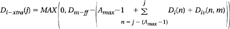
The request access distance statistic can be used to compute maximum bandwidth efficiency for a workload subjected to different DRAM row cycle times and device data rates. Figure 15.10 shows how maximum bandwidth efficiency can be computed for a request stream in a close-page memory system. In Figure 15.10, the request stream has been simplified down to the sequence of bank IDs. The access distances for each request are then computed from the sequence of bank IDs. The example illustrated as Figure 15.10 specifies that a minimum of eight requests needs to be active at any given instance in time in order to achieve full bandwidth utilization. In terms of access distances, each pair of accesses to the same bank needs to have seven other accesses in between them. At the beginning of the sequence in Figure 15.10, a pair of requests needs to access bank 0 with only four other requests to different banks in between them. As a result, an idling distance of 3 must be added to the access sequence before the second request to bank 0 can be processed. Two requests later, the request to bank 2 has an access distance of 5. However, idling distances added to requests in between accesses to bank 2 also count toward its effective total access distance. The result is that the total access distance for the second access to bank 2 is 8, and no additional idling distances ahead of the access to bank 2 are needed. Finally, after all idling distances have been computed, the maximum bandwidth efficiency of the access sequence may be computed by dividing the total number of requests by the sum of the total number of requests and all of the idling distances. In the example shown in Figure 15.10, the maximum sustained bandwidth efficiency is 54.2%.

15.3.7 An Applied Example for an Open-Page System
In this section, an example is used to illustrate the process for obtaining maximum sustainable bandwidth in an open-page memory system. Figure 15.11 shows a request stream that has been simplified down to a sequence of bank IDs and row IDs of the individual requests, and the access distances are then computed from the sequence of bank IDs and row IDs. The example illustrated in Figure 15.10 specifies that a minimum of nine requests need to be active at any given instance in time in order to achieve full bandwidth utilization, and there must be eight requests between row activations as well as four requests between bank conflicts. Figure 15.11 shows that Di-ff(j) and Di-lf(j) are separately computed, but the idling distance Di(j) is simply the maximum of Di-ff(j) and Di-lf(j). After all idling distances have been computed, the maximum bandwidth efficiency of the request sequence can be computed by dividing the total number of requests by the sum of the total number of requests and all of the idling distances. In the example shown in Figure 15.11, the maximum sustained bandwidth efficiency is 56.1%.
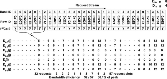
Finally, one caveat that must be noted in the examples shown in Figures 15.10 and 15.11 is that the request access distances and idling distances illustrated are integer values. However, data transport times and row cycle times seldom divide evenly as integer values, and the respective values are often real numbers rather than simple integer values.
15.3.8 System Configuration for RAD-Based Analysis
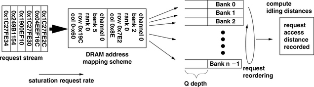
The RAD analytical framework is used in this section to compute the maximum bandwidth efficiency of DRAM memory systems. However, the bandwidth efficiency of any DRAM memory system is workload specific and sensitive to the organization of the DRAM memory system and the scheduling policy of the memory controller. Figure 15.12 shows the general system configuration used in the RAD analytical framework, where requests within a request stream are subjected to an address mapping scheme and mapped to a specific DRAM channel, rank, bank, row, and column address. The requests can then be reordered to a limited degree, just as they may be reordered in a high-performance memory controller to minimize the amount of idling times that must be inserted into the request stream to satisfy the constraints imposed by DRAM protocol overheads, DRAM bank row cycle times, and tFAW row activation limitations.
In this study, the DRAM memory bandwidth characteristics of eight different DRAM memory system configurations are subjected to varying data rate scaling trends and tFAW row activation constraints. Table 15.5 summarizes the different system configurations used in this study. The eight different system configurations consist off our open-page memory systems and four close-page memory systems. In the open-page memory systems, consecutive cacheline addresses are mapped to the same row in the same bank to optimize hits to open row buffers. In the close-page memory systems, consecutive cacheline addresses are mapped to different banks to optimize for bank access parallelism. Aside from the difference in row-buffer-management policies and address mapping schemes, two of the four close-page memory systems also support transaction reordering. In these memory systems, transaction requests are placed into queues that can enqueue as many as four requests per bank. Transaction requests are then selected out of the reordering queues in a round-robin fashion through the banks to maximize the temporal scheduling distance between requests to a given bank. In this study, the memory systems are configured with 1 or 2 ranks of DRAM devices, and each rank of DRAM devices has either 8 or 16 banks internally. The eight respective system configurations in Table 15.1 are described in terms of the paging policy, reordering depth, rank count, and bank count per rank. For example, open-F-1-8 represents an open-page system with no transaction reordering, 1 single rank in the system, and 8 banks per rank. Finally, all of the systems have 16384 rows per bank and 1024 columns per row.

This study examines the maximum sustainable bandwidth characteristics of modern DRAM memory systems with data rates that range from 533 to 1333 Mbps. Furthermore, one assumption made in the studies in this section is that the device data rate of the DRAM devices is twice that of the operating frequency of the DRAM device. Therefore, the operating frequency of the memory system examined in this study ranges from 266 to 667 MHz, and the notion of a clock cycle corresponds to the operating frequency of the DRAM device. Throughout this study, the row cycle time of the DRAM devices is assumed to be 60 ns. The rank-to-rank turnaround time, tRTRS, is set to either 0 or 3 clock cycles. Furthermore, tCWD is set to 3 clock cycles, tCMD is set to 1 clock cycle, tWR is set to 4 clock cycles, tBRUST is set to 4 clock cycles, and tCAS is set to 4 clock cycles. Finally, the tFAW row activation constraint is set to the extreme values of either 30 or 60 ns. That is, tFAW is set to equal tRC or tRC/2, where tFAW equal to tRC is assumed to be a worst-case value for tFAW, and tFAW equal to tRC/2 is assumed to an optimistic best-case value for proposed tFAW constraints.
15.3.9 Open-Page Systems: 164.gzip
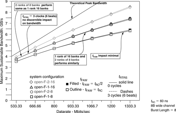
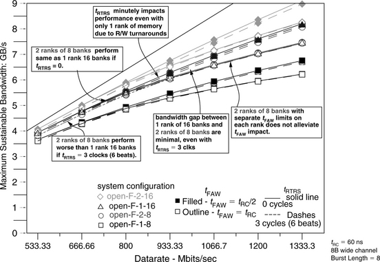
Figure 15.13 shows the computed maximum bandwidth efficiency of four different open-page memory systems for the 164.gzip address trace. Figure 15.13 shows that with a constant row cycle time of 60 ns, the maximum bandwidth efficiency of the DRAM memory system gradually decreases as a function of increasing data rate. For the address trace from 164.gzip, factors such as a restrictive tFAW value and the rank-to-rank turnaround time have only minimum impact on available DRAM bandwidth, illustrating a fair degree of access locality and resulting in open-page hits and fewer row accesses. Finally, Figure 15.13 shows that the additional parallelism afforded by the 2 rank, 16 bank (2R16B) memory system greatly improves bandwidth efficiency over that of a 1 rank, 8 bank (1R8B) memory system.

Figure 15.13 shows the maximum bandwidth available to the address trace of 164.gzip in terms of maximum bandwidth efficiency. Figure 15.14 shows the same data as Figure 15.13, but represents the data in terms of sustainable bandwidth by assuming a specific system configuration with an 8-byte-wide data bus. With the 8-byte-wide data bus operating at different data rates, the theoretical peak bandwidth available to the DRAM memory system is shown as a solid line labelled as peak bandwidth in Figure 15.14. Figures 15.13 and 15.14 show that 164.gzip is an outlier in the sense that the workload has a high degree of access locality, and a large majority of the requests are kept within the same rank of memory systems. In the case where DRAM accesses are made to a different rank, a bank conflict also follows. As a result, the impact of tRTRS is not readily observable in any system configuration, and a 2 rank, 8 bank (2R8B) system performs identically to a 1 rank, 16 bank (1R16B) memory system. Also, the number bank conflicts are relatively few, and the impact of tFAW is minimal and not observable until data rates reach significantly above 1 Gbps. Finally, the maximum sustainable bandwidth for 164.gzip scales nicely with the total number of banks in the memory system, and the bandwidth advantage of a 2R16B memory system over that of a 1R16 memory system is nearly as great as the bandwidth advantage of the 1R16B memory system over that of a 1R8B memory system.
15.3.10 Open-Page Systems: 255.vortex
Figure 15.15 shows the maximum sustainable bandwidth characteristic of 255.vortex in open-page memory systems. Figure 15.15 shows that in contrast to the maximum sustainable bandwidth characteristics shown by the address trace of 164.gzip in Figure 15.14, 255.vortex is an outlier that is not only sensitive to the system configuration in terms of the number of ranks and banks, but it is also extremely sensitive to the impacts of tFAW and tRTRS. Figure 15.15 also shows that the address trace of 255.vortex has relatively lower degrees of access locality, and fewer column accesses are made to the same row than other workloads, resulting in a relatively higher rate of bank conflicts. The bank conflicts also tend to be clustered to the same rank of DRAM devices, even in 2-rank system configurations. The result is that the tFAW greatly limits the maximum sustainable bandwidth of the DRAM memory system in all system configurations.

Figure 15.15 shows that 255.vortex is greatly impacted by the rank-to-rank switching overhead, tRTRS, in system configurations with 2 ranks of memory. The overhead attributable to tRTRS is somewhat alleviated at higher data rates, as other limitations on available memory system bandwidth become more significant. At higher data rates, the bandwidth impact of tRTRS remains, but the effects become less discernible as a separate source of hindrance to data transport in a DRAM memory system. Furthermore, Figure 15.15 shows an interesting effect in that the rank-to-rank switching overhead, tRTRS, can also impact the performance of a single rank memory system due to the fact that tRTRS contributes to the read-write turnaround time, and the contribution of tRTRS to the read-write turnaround time can be observed in Table 15.3. Finally, Figure 15.15 shows the impact of tFAW on 255.vortex, where the simulation assumption of tFAW = tRC completely limits sustainable bandwidth for all system configurations beyond 800 Mbps. At data rates higher than 800 Mbps, no further improvements in maximum sustainable bandwidth can be observed for the address trace of 255.vortex in all tFAW limited memory systems.
15.3.11 Open-Page Systems: Average of All Workloads
Figures 15.14 and 15.15 show the maximum sustainable bandwidth characteristics of 164.gzip and 255.vortex, two extreme outliers in the set of workloads listed in Table 15.1 in terms of sensitivity to system configuration and timing parameters. That is, while the address trace of 164.gzip was relatively insensitive to the limitations presented by tRTRS and tFAW, the address trace for 255.vortex was extremely sensitive to both tRTRS and tFAW Figure 15.16 shows the maximum sustainable bandwidth averaged across all workloads used in the study. Figure 15.16 shows that for the open-page memory system, the high degree of access locality provided by the address traces of the various single threaded workloads enables the open-page systems to achieve relatively high bandwidth efficiency without the benefit of sophisticated transaction request reordering mechanisms. Figure 15.16 also shows that the open-page address mapping scheme, where consecutive cacheline addresses are mapped to the same row address, effectively utilizes parallelism afforded by the multiple ranks, and the performance of a 2R8B memory system is nearly equal to that of a 1R16B memory system. The bandwidth degradation suffered by the 2R8B memory system compared to the 1R16B memory system is relatively small, even when the rank-to-rank switching overhead of tRTRS equals 3 clock cycles. The reason for this minimal impact is that the access locality of the single threaded workloads tend to keep accesses to within a given rank, and rank-to-rank switching time penalties are relatively minor or largely hidden by row cycle time impacts.
One surprising result shown in Figure 15.16 is that the four-bank activation window constraint, tFAW, negatively impacts the sustainable bandwidth characteristic of a two-rank memory system just as it does for a one-rank memory system. This surprising result can be explained with the observation that the address mapping scheme, optimized to obtain bank parallelism for the open-page row-buffer-management policy, tends to direct accesses to the same bank and the same rank. In this scheme, bank conflicts are also often directed onto the same rank in any given time period. The result is that multiple row cycles tend to congregate in a given rank of memory, rather than become evenly distributed across two different ranks of memory, and tFAW remains a relevant issue of concern for higher performance DRAM memory systems, even for a dual rank memory system that implements the open-page row-buffer-management policy.
Finally, Figure 15.16 shows that the impact of tRTRS is relatively constant across different data rates for systems that are not impacted by tFAW. A close examination of the bandwidth curves for the 2R16B system reveals that in systems impacted by tFAW limitations, the impact of tRTRS is mitigated to some extent. That is, idle cycles inserted into the memory system due to rank-to-rank switching times can be used to reduce the addition of more idle times as needed by DRAM devices to recover between consecutive row accesses. In that sense, the same idle cycles can be used to satisfy multiple constraints, and the impact of these respective constraints are not strictly additive.
15.3.12 Close-Page Systems: 164.gzip
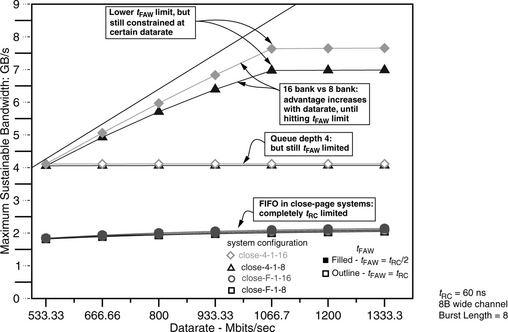
Figure 15.17 shows the maximum bandwidth available to the address trace of 164.gzip for the four different close-page memory systems listed in Table 15.5. Figure 15.17 shows that for the address trace of 164.gzip in close-page memory systems without transaction reordering, the maximum sustainable bandwidth increases very slowly with respect to increasing data rate of the memory system, and neither the number of banks available in the system nor the tFAW parameter has much impact. However, Figure 15.17 also shows that in close-page memory systems with a reorder queue depth of 4, representing memory systems with relatively sophisticated transaction reordering mechanisms, the memory system can effectively extract available DRAM bandwidth for the address trace of 164.gzip. In the case where tFAW equals tRC/2, the sustained bandwidth for the address trace of 164.gzip continues to increase until the data rate of the DRAM memory system reaches 1.07 Gbps. At the data rate of 1.07 Gbps, the ratio of tRC to tBURST equals the maximum number of concurrently open banks as specified by the ratio of tFAW to tRC, and the maximum sustained bandwidth reaches a plateau for all system configurations. However, Figure 15.17 also shows that in the case where tFAW equals tRC, the DRAM memory system can only sustain 4 GB/s of bandwidth for the 164.gzip address trace regardless of data rate since tfaw severely constrains the maximum number of concurrently open banks in close-page memory systems. Finally, Figure 15.17 shows the performance benefit from having 16 banks compared to 8 banks in the DRAM memory system. Figure 15.17 shows that at low data rates, the performance benefit of having 16 banks is relatively small. However, the performance benefit of 16 banks increases with increasing data rate until the tFAW constraint effectively limits the available DRAM bandwidth in the close-page memory system.
15.3.13 Close-Page Systems: SETI@HOME Processor Bus Trace
Figure 15.18 shows the maximum sustainable bandwidth graph for a short trace captured on the processor bus with a digital logic analyzer while the host processor was running the SETI@HOME application. Similar to the bandwidth characteristics of the 164.gzip address trace shown in Figure 15.17, Figure 15.18 shows that the SETI@HOME address trace is completely bandwidth bound in cases where no transaction reordering is performed. However, differing from the bandwidth characteristics of the 164. gzip address trace shown in Figure 15.17, Figure 15.18 shows that in close-page memory systems that perform transaction reordering, the SETI@HOME address trace benefits greatly from a memory system with a 16-bank device. Figure 15.18 shows that a highly sophisticated close-page 1R16B memory system can provide nearly twice the bandwidth compared to the same memory system with a 1R8B configuration. In this respect, the SETI@HOME address trace is an outlier that benefits greatly from the larger number of banks.

FIGURE 15.18 Maximum sustainable bandwidth of the SETI@HOME address trace: close-page systems.
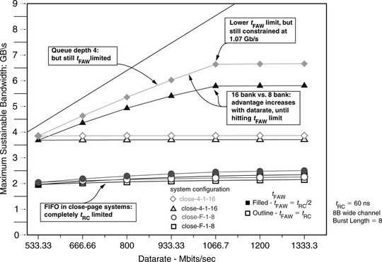
15.3.14 Close-Page Systems: Average of All Workloads
Figure 15.19 shows the maximum sustainable bandwidth that is the average of all workloads listed in Table 15.1. Figure 15.19 shows that the all workloads average graph is similar to the maximum sustainable bandwidth graph shown for the address trace of 164.gzip in Figure 15.17 with some minor differences. Similar to Figure 15.17, Figure 15.19 shows that in close-page memory systems without transaction reordering, the maximum sustainable bandwidth of the DRAM memory system increases very slowly with respect to increasing data rate of the memory system, and neither the number of banks available in the system nor the tFAW parameter shows much impact. However, Figure 15.19 also shows that in close-page memory systems with a reorder queue depth of 4, the memory system can effectively extract available DRAM bandwidth across different workloads. Figure 15.19 further shows that similar to the maximum sustainable bandwidth characteristics for the address traces of 164.gzip and SETI@HOME, the maximum sustained bandwidth for the average workload continues to increase until the data rate of the DRAM memory system reaches 1.07 Gbps in the case that tFAW equals tRC/2. Finally, Figure 15.19 shows that the bandwidth advantage seen by the average workload is closer to that shown by the 164.gzip address trace in Figure 15.17 than the SETI@HOME address trace in Figure 15.18, and the bandwidth advantage of the 1R16B configuration increases with increasing data rate until the tFAW constraint effectively limits the available DRAM bandwidth in the close-page memory system.
15.3.15 tFAW Limitations in Open-Page System: All Workloads
Figures 15.17, 15.18, and 15.19 collectively illustrate the point that close-page memory systems are very sensitive to the row activation limitations presented by tFAW. The simple explanation is that in a single rank, close-page memory system, tFAW defines the maximum number of banks that can be open concurrently for access, and once that limit is reached, no further scaling in utilizable bandwidth is possible regardless of the data rate of the memory system. However, in open-page memory systems, there are likely multiple column accesses for each row access, and the limitation on the number of row activations per unit time presented by tFAW is more difficult to quantify. Figure 15.20 shows the impact of tFAW in a 1R16B memory system in terms of the percentage of bandwidth differential between the case where tFAW = tRC = 60 ns and the case where tFAW = tRC/2 = 30 ns. The bandwidth differential curves for different workloads used in the simulation are drawn as separate lines in Figure 15.20, illustrating the wide variance in workload sensitivity to the limitation presented by a restrictive tFAW parameter. One workload worthy of note is 255.vortex, where bandwidth impact for the case of tFAW = 60 ns reduces available bandwidth by upwards of 30% at data rates above 1.2 Gbps. However, on average, a workload running on a memory system where tFAW = 60 ns suffers a bandwidth loss on the order of 0∼12% compared to the same system with a less restrictive tFAW value where tFAW = 30 ns.

15.3.16 Bandwidth Improvements: 8-Banks vs. 16-Banks
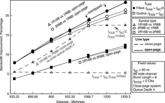
Figure 15.21 examines the bandwidth advantage of a 16-bank device over that of an 8-bank device. Figure 15.21 shows mean bandwidth improvement curves for the 1R16B versus 1R8B comparison for the open-page memory system and the close-page memory system with a per-bank reordering queue depth of 4. Figure 15.21 also shows the mean bandwidth improvement curves for the 2R8B versus 1R8B and 2R16B versus 2R8B comparisons for open-page memory systems. Figure 15.21 shows that despite the differences in the row-buffer-management policy and the differences in the reordering mechanism, the bandwidth advantage of a 1R16B memory system over that of a 1R8B memory system correlates nicely between the open-page memory system and the close-page memory system. In both cases, the bandwidth advantage of having more banks in the DRAM device scales at roughly the same rate with respect to increasing data rate and constant row cycle time. In both open-page and close-page memory systems, the bandwidth advantage of the 1R16B memory system over that of the 1R8B memory system reaches approximately 18% at 1.07 Gbps. However, Figure 15.21 also shows that at 1.07 Gbps, close-page memory systems become bandwidth limited by the restrictive tFAW value, while the bandwidth advantage of the 1R16B memory system continues to increase with respect to increasing data rate, reaching 22% at 1.33 Gbps. Finally, Figure 15.21 shows that with a 2-rank configuration, the bandwidth advantage afforded by a 16-bank DRAM device over that of an 8-bank device is nearly halved, and the bandwidth advantage of a 2R16B system configuration over that of a 2R8B system configuration reaches 12% at 1.33 Gbps.
A study of DRAM memory system bandwidth characteristics based on the RAD analytical framework is performed in this section. As reaffirmed in this section, the performance of DRAM memory systems depends on workload-specific characteristics, and those workload-specific characteristics exhibit large variances from each other. However, some observations about the maximum sustainable bandwidth characteristics of DRAM memory systems can be made in general.
• The benefit of having a 16-bank device over an 8-bank device in a 1-rank memory system configuration increases with data rate. The performance benefit increases to approximately 18% at 1 Gbps for both open-page and close-page memory systems. While some workloads may only see minimal benefits, others will benefit greatly. Embedded systems with a single rank of DRAM devices and limited in the variance of workload characteristics should examine the bank count issue carefully.
• Single threaded workloads have high degrees of access locality, and sustainable bandwidth characteristics of an open-page memory system for a single threaded workload are similar to that of a close-page memory system that performs relatively sophisticated transaction reordering.
• The tFAW activation window constraint greatly limits the performance of close-page memory systems without sophisticated reordering mechanisms. The impact of tFAW is relatively less in open-page memory systems, but some workloads, such as 255. vortex, apparently contain minimal spatial locality in the access sequences, and their performance characteristics are similar to that of workloads in close-page memory systems. In this study, even a two-rank memory system did not alleviate the impact of tFAW on the memory system. Consequently, a DRAM scheduling algorithm that accounts for the impact of tFAW is needed in DRAM memory controllers that may need to handle workloads similar to 255.vortex.
The RAD analytical framework is used in this section to examine the effect of system configurations, command scheduling algorithms, controller queue depths, and timing parameter values on the sustainable bandwidth characteristics of different types of DRAM memory systems. However, the analytical framework-based analysis is limiting in some ways, and a new simulation framework, DRAMSim, was developed at the University of Maryland to accurately simulate the interrelated effects of memory system configuration, scheduling algorithms, and timing parameter values. The remainder of the chapter is devoted to the study of memory system performance characteristics using the DRAMSim simulation framework.
15.4 Simulation-Based Analysis
In the previous section, the equation-based RAD analytical framework was used to examine the respective maximum sustainable bandwidth characteristics of various DRAM memory system configurations. The strength of the RAD analytical framework is that it can be used as a mathematical basis to construct a first-order estimate of memory system performance characteristics. Moreover, the accuracy of the RAD analytical framework does not depend on the accuracy of the simulation model, since the basis of the framework relies on the set of equations that can be separately examined to ensure correctness. However, the weakness of the RAD analytical framework is that it is limited to specific controller scheduling algorithms and saturation request rates to examine the sustainable bandwidth characteristics of a given memory system, and it cannot be used to analyze a wide range of controller scheduling policies, memory-access latency distribution characteristics, and controller queue depth examinations. To remedy this shortcoming, the more traditional approach of a simulator-based analytical framework is used in this section to examine memory system performance characteristics.
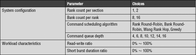
15.4.1 System Configurations
The basis of the simulation work performed in this section is a highly accurate DRAM memory simulator, DRAMSim. In this section, the impact of varying system configurations, DRAM device organizations, read-versus-write traffic ratios, and protocol-constraining timing parameters that affect memory system performance characteristics in DDR2 SDRAM and DDR3 SDRAM memory systems are examined with the DRAMSim memory system simulator. The studies performed in this section are more generally based on random address workloads—the study on latency distribution characteristics excepted—so parameters such as the read-versus-write traffic ratio can be independently adjusted. Table 15.6 summarizes the four different system configuration parameters and two workload characteristics varied in this section for the study on the sustainable bandwidth characteristics of high-speed memory systems. The hardware architecture and various parameters of the simulated DRAM memory system and workload characteristics in terms of read-write ratios and differing burst lengths are described in the following sections.
15.4.2 Memory Controller Structure
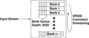
In contrast to the basic controller structure assumed in the studies performed in the previous sections using the RAD analytical framework, the DRAMsim simulator uses a more generic memory controller model to schedule DRAM commands rather than memory transactions. The ability to schedule DRAM commands separately ensures that the controller can obtain the highest performance from the DRAM memory system. Figure 15.22 illustrates the basic hardware architecture of a single channel memory controller assumed in this section. In the controller structure illustrated in Figure 15.22, transactions are translated into DRAM commands and placed into separate queues that hold DRAM commands destined for each bank.2 The depth of the per-bank queues is a parameter that can be adjusted to test the effect of queue depth on maximum sustainable bandwidth of the memory system. The basic assumption for the memory controller described in Figure 15.22 is that each per-bank queue holds all of the DRAM commands destined for a given bank, and DRAM commands are executed in FIFO order within each queue. In the architecture illustrated in Figure 15.22, a DRAM command scheduling algorithm selects a command from the head of the per-bank queues and sends that command to the array of DRAM devices for execution. In this manner, the controller structure described in Figure 15.22 enables the implementation of aggressive memory controller designs without having to worry about write-to-read ordering issues. That is, since read and write transactions destined for any given bank are executed in order, a read command that semantically follows a write command to the same address location cannot be erroneously reordered and scheduled ahead of the write command. On the other hand, the controller structure allows an advanced memory controller to aggressively reorder DRAM commands to different banks to optimize DRAM memory system bandwidth. Finally, the queue depth in the simulated controller structure describes the depth of the queue in terms of DRAM commands. In a close-page memory system, each transaction request converts directly to two DRAM commands: a row access command and a column-access-with-auto-precharge command.
15.4.3 DRAM Command Scheduling Algorithms
In the studies performed in this section, sustainable bandwidth characteristics of four DRAM command scheduling algorithms for close-page memory systems are compared. The four DRAM command scheduling algorithms are Bank Round-Robin (BRR), Rank Round-Robin (RRR), Wang Rank Hop (Wang), and Greedy. The role of a DRAM command scheduling algorithm is to select a DRAM command at the top of a per-bank queue and send that command to the DRAM devices for execution. In a general sense, the DRAM command scheduling algorithm should also account for transaction ordering and prioritization requirements. However, the study on the DRAM command scheduling algorithm is narrowly focused on the sustainable bandwidth characteristics of the DRAM memory system. consequently, all transactions are assumed to have equal scheduling priority in the following studies.
Bank Round-Robin (BRR)
The Bank Round-Robin (BRR) command scheduling algorithm is a simple algorithm that rotates through the per-bank queues in a given rank sequentially and then moves to the next rank. The BRR algorithm is described as follows:
• The row access command and the column-access-with-precharge command are treated as a command pair. The row access and column-access-with-precharge command pair are always scheduled consecutively.
• Due to the cost of write-to-read turnaround time in DDR3 devices, implicit write sweeping is performed by scheduling only read transactions or write transactions in each loop iteration through all banks in the system.
• The BRR algorithm goes through the per-bank queues of rank i and looks for transactions of a given type (read or write). If a given queue is empty or has a different transaction type at the head of the queue, BRR skips over that queue and goes to bank (j + 1) to look for the next candidate.
• When the end of rank i is reached, switch to rank ((i + 1) % rank_count) and go through the banks in that rank.
• If the rank and bank IDs are both 0, switch over the read/write transaction type. Consequently, BRR searches for read and write transactions in alternating iterations through all banks and ranks in the memory system.
Rank Round-Robin
The Rank Round-Robin (RRR) command scheduling algorithm is a simple algorithm that rotates through per-bank queues by going through all of the rank IDs for a given bank and then moves to the next bank. In a single-rank memory system, RRR and BRR are identical to each other. The RRR algorithm is described as follows:
• The RRR algorithm is identical to the BRR algorithm except that the order of traversal through the ranks and banks is reversed. That is, after the RRR algorithm looks at bank j of rank i for a candidate to schedule, it then moves to bank j of rank (i + 1) instead of bank (j + 1) of bank i. In the case where rank i is the highest rank ID available in the system, the bank ID is incremented and the process continues.
• DRAM command pairs for a given transaction are always scheduled consecutively, just as in BRR.
• Just as in BRR, if the rank ID and bank ID are both 0, RRR switches over the read/write transaction type. In this manner, RRR searches for read transactions and write transactions in alternating iterations through all banks and ranks in the memory system.
Wang Rank Hop (Wang)
The Wang Rank Hop (Wang) command scheduling algorithm is a scheduling algorithm that requires the presence of at least two ranks of DRAM devices that share the data bus in the DRAM memory system, and it alleviates timing constraints imposed by tFAW, tRRD, and tRTRS by distributing row activation commands to alternate ranks of DRAM devices while group scheduling column access commands to a given rank of DRAM devices. In contrast to the BRR and RRR scheduling algorithms, the Wang algorithm requires that the row access command and the column-access-with-precharge command be separated and scheduled at different times.
Figure 15.23 illustrates an idealized, best-case timing diagram for the Wang algorithm. Figure 15.23 shows that the row access (row activation) commands are sent to alternate ranks to avoid incurring the timing penalties associated with tFAW and tRRD, and column access commands are group scheduled to a given rank of DRAM devices. Ideally, rank switching only occurs once per N column access commands, where N is the number of banks in the DDR3 DRAM device.
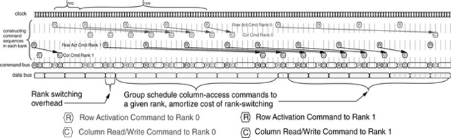
FIGURE 15.23 Idealized timing diagram for the Wang Rank Hop algorithm in a dual rank, 8 banks per rank system.
One simple way to implement the Wang algorithm is to predefine a command sequence so that the row access commands are sent to alternating ranks and the column access commands are group scheduled. Figure 15.24 illustrates two simple command scheduling sequences for dual rank systems with 8 banks per rank and 16 banks per rank, respectively. Although the sequences illustrated in Figure 15.24 are not the only sequences that accomplish the scheduling needs of the Wang algorithm, they are the simplest, and other subtle variations of the sequences do not substantially improve the performance of the algorithm. The Wang command schedule algorithm is described as follows:

FIGURE 15.24 Command scheduling sequence for the Wang Rank Hop algorithm for devices with 8 and 16 banks.
• Follow the command sequence as defined in Figure 15.24. Select a row access command for issue if and only if the column access command that follows is the correct type for the current sequence iteration. If the column access command for that queue is the wrong type, or if the queue is empty, skip that queue and go to next command in the sequence.
• If rank ID and bank ID are both 0, switch over the read/write type and continue the sequence.
Greedy
The Greedy command scheduling algorithm differs from the BRR, RRR, and Wang command scheduling algorithms in that these other algorithms are based on the notion that commands are selected for scheduling based on a logical sequence of progression through the various banks and ranks in the memory system, while the Greedy algorithm does not depend on a logical sequence to select commands for scheduling. Instead, the Greedy algorithm examines pending commands at the top of each per-bank queue and selects the command that has the smallest wait-to-issue time. That is, after commands are selected in the BRR, RRR, and Wang command scheduling algorithms, the memory controller must still ensure that the selected command meets all timing constraints of the DRAM memory system. In contrast, the Greedy algorithm computes the wait-to-issue time for the command at the head of each per-bank queue and then selects the command with the smallest wait-to-issue time regardless of the other attributes of that command. In the case where two or more commands have the same wait-to-issue time, a secondary factor is used to select the command that will be issued next. In the current implementation of the Greedy algorithm, the age of the competing commands is used as the secondary factor, and the Greedy algorithm gives preference to the older command. Alternatively, the Greedy command scheduling algorithm can use other attributes as the secondary factor in the selection mechanism. For example, in the case where two column access commands are ready to issue at the same time, a variant of the Greedy algorithm can allow the column read commands to proceed ahead of column write commands. Alternatively, the concept of queue pressure can be used to allow the command in the queue with more pending commands to proceed ahead of commands from queues with fewer pending commands. These subtle modifications can minutely improve upon the sustainable bandwidth characteristics of the Greedy algorithm. However, these other variants may introduce problems of their own, such as starvation. These issues must be addressed in a Greedy scheduling controller. Consequently, the Greedy algorithm must be complemented with specific anti-starvation mechanisms.
The Greedy algorithm as simulated in DRAMSim2 is described as follows:
• Compute the wait-to-issue time for the command at the head of each per-bank queue.
• Select the command with the smallest wait-to-issue time regardless of all command attributes—type, age, or address IDs.
• In the case where two or more commands have the same, shortest wait-to-issue time, select the oldest command from the set.
15.4.4 Workload Characteristics
In this work, a random number generator is used to create transaction request sequences that drive the simulated DRAM memory systems. A study is performed in this section to compare the bandwidth efficiency of memory systems as a function of burst length and queue depth, culminating in figure 15.25. The simulation conditions are described in this section. For this study, a random number generator is used to create transaction request sequences, that drive the simulated DRAM memory systems. In general, transaction request sequences possess three attributes that can greatly impact the sustainable bandwidth characteristics of the closed-page DRAM memory systems examined in this section. The three attributes are the address locality and distribution characteristics of the transaction request sequence, the read-to-write ratio of the transaction request sequence, and the ratio of short burst requests in the transaction request sequence. These attributes are described in detail here.
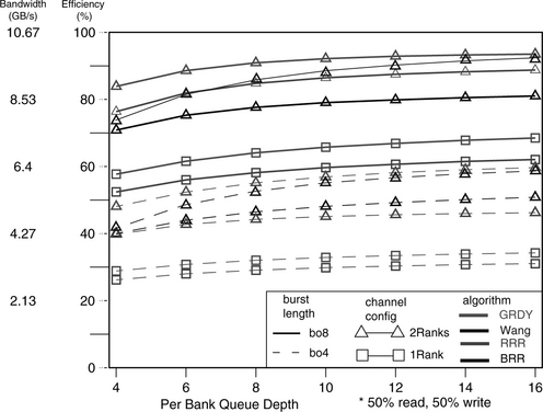
FIGURE 15.25 Bandwidth efficiency and sustainable bandwidth as a function of burst length and queue depth.
Address Distribution
In this study, requests within the input stream are equally distributed to all banks in the memory system. So the probability of a transaction request hitting a given bank is inversely proportional to the total number of banks in the DRAM memory system. Moreover, the address generation process is memoryless so that the address of each transaction is not dependent on the addresses of previous transactions. Although the capability to specify locality characteristics exists in the simulator, it is not used in this study.
Read Transaction Percentage
In this study, the random number generator is also used to select the read or write type of transaction in the input stream. In this study, the ratio of read transactions to write transactions is used as a variable parameter, and it can be adjusted by specifying the percentage of read requests in the transaction request sequence. In the request sequence used in this study, all transactions that are not read transactions are write transactions. Consequently, a transaction request sequence that has 0% read transactions consists of 100% write transactions.
Short Burst Request Percentage
The prefetch length of DDR3 SDRAM devices is 8. In the case where fewer than 8 beats of data are needed, an 8-beat burst can be chopped so that only 4 beats of data are transmitted by the DDR3 SDRAM device. In this study, the percentage of short, burst-length-of-4 (Bo4) requests can be specified as a variable parameter. The basic assumption used in this study is that the percentage of read transactions is the same for burst-length-of-4 (bo4) and burst-of-8 (bo8) transaction requests.
15.4.5 Timing Parameters
The timing parameters used in DRAMSim for the study of high-speed DRAM memory systems are summarized in Table 15.7. The parameters have been chosen to generally model a high-speed, high-performance DDR3 SDRAM memory system operating at 1.33 Gbps with tCAS, tRCD, and tRP timing of 6-6-6. In the studies performed in this section, the maximum sustainable bandwidths of different system configurations are compared at the data rate of 1.33 Gbps. The preliminary timing parameter values assumed in this study for the 1.33 Gbps DDR3 SDRAM memory system are listed in Table 15.7 in terms of number of cycles. Since the base frequency of the 1.33-Gbps DDR3 SDRAM memory system is 667 MHz, 1 cycle in the 1.33 Gbps memory system is exactly 1.5 ns in duration.
TABLE 15.7
Summary of timing parameters used in a generic DRAM-access protocol
| Parameter | Description | @Cycles 1.33 Gbps |
| tAL | Added Latency to column accesses, used in DDRx SDRAM devices for posted CAS commands. | 5 |
| tBURST | Data burst duration. The number of cycles that data burst occupies on the data bus. In DDRx SDRAM, 4 beats = 2 cycles. | 2 or 4 |
| tCAS | Column Access Strobe latency. The time interval between column access command and the start of data return by the DRAM device(s). | 8 |
| tCCD | Column-to-Column Delay. The minimum intra-device column-to-column command timing, determined by internal prefetch length. | 4 |
| tCMD | Command transport duration. The time period that a command occupies on the command bus. | 1 |
| tCWD | Column Write Delay. The time interval between issuance of a column write command and data placement on a data bus by the controller. | 5 |
| tFAW | Four (row) bank Activation Window. A rolling time-frame in which a maximum of four bank activation can be initiated. | 20 |
| tOST | ODT Switching Time. The time interval to switching ODT control from rank to rank. (Assume termination scheme for 0 cycle ODT switching.) | 0 |
| tRAS | Row Access Strobe. The time interval between a row access command and data restoration in a DRAM array. | 18 |
| tRC | Row Cycle. The time interval between accesses to different rows in a bank. tRC tRAS + tRP | 24 |
| tRCD | Row to Column command Delay. The time interval between row access and data ready at sense amplifiers. | 6 |
| tRFC | Refresh Cycle Time. The time interval between Refresh and Activation commands. | − |
| tRP | Row Precharge. The time interval that it takes for a DRAM array to be precharged for another row access. | 6 |
| tRRD | Row activation to Row activation Delay. The minimum time interval between two row activation commands to the same DRAM device. | 4 |
| tRTP | Read to Precharge. The time interval between a read and a precharge command. Can be approximated by tCAS − tCMD. | 5 |
| tRTRS | Rank-to-rank switching time. Used in DDR and DDR2 SDRAM memory systems. | 1 ∼ 3 |
| tWR | Write Recovery time. The minimum time interval between the end of write data burst and the start of a precharge command. | 6 |
| tWTR | Write To Read delay time. The minimum time interval between the end of write data burst and the start of a column read command. | 5 |
15.4.6 Protocol Table
DRAMSim2 uses a protocol table to simulate timing constraints between pairs of DRAM commands in a DRAM memory system, and the protocol table is shown in Table 15.8. Table 15.8 is organized by each DRAM command and the possible commands that can precede each respective command. The table specifies the respective minimum timing constraints between each command pair in terms of an equation of timing parameters. The timing equations used in Table 15.8 can be independently verified against timing specifications given in various DRAM device data sheets, and the literal implementation of the protocol table in DRAMSim2 ensures that the timing relationships specified in DRAM device data sheets are observed with absolute accuracy. Table 15.8 summarizes the minimum timing equations for basic DRAM command interactions between row access, column read, column write, precharge, and refresh commands.
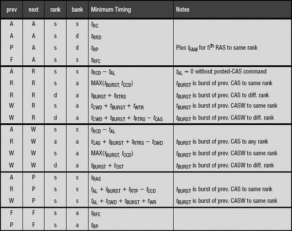
15.4.7 Queue Depth, Scheduling Algorithms, and Burst Length
Figure 15.25 shows simulation results for various scheduling algorithms with different system configurations. In Figure 15.25, the bandwidth efficiency and the associated bandwidth of an 8-byte-wide, 1.33 Gbps DDR3 memory system are respectively characterized at different queue depths, with different system configurations and different scheduling algorithms. Figure 15.25 shows that the Greedy DRAM command scheduling algorithm achieves the highest bandwidth efficiency over all other scheduling algorithms and system configurations. Figure 15.25 also shows that sustainable bandwidth increases with deeper queue depths for nearly all algorithms and all system configurations, but the bandwidth typically plateaus at a queue depth of 10.
Figure 15.25 shows that the available bandwidth of a high-speed DDR3 memory system drops dramatically when the traffic consists of short, bo4 requests. Due to the fact that tCCD is 4 cycles and tRRD is also 4 cycles, short bo4 requests cannot be pipelined from a single rank of DRAM devices, and the highest available bandwidth can be obtained from a system with multiple ranks of DRAM devices. However, even in the case where two ranks of DRAM devices exist in the memory system, the rank-to-rank switching time effectively limits the peak bandwidth efficiency of the memory system to 66.7%. However, due to the existence of other bandwidth-constraining timing parameters, Figure 15.25 also shows that the highest performance, two-rank, 1.33 Gbps DDR3 SDRAM memory system merely approaches 60% bandwidth efficiency.
Finally, one issue not specifically illustrated in Figure 15.25 is that the Greedy algorithm is not itself an algorithm that guarantees fairness. Whereas BRR, RRR, and Wang algorithms all guarantee that a request will be serviced within a predictable number of cycles upon entering a queue of a given depth, a request can, in theory, be deferred for an indefinitely long period of time. Consequently, the Wang algorithm may be preferred in certain high-performance applications where an anti-starvation requirement must be guaranteed by the scheduling algorithm.
15.4.8 Effect of Burst Length on Sustainable Bandwidth
Figure 15.25 shows that the sustainable bandwidth of the high-speed DDR3 SDRAM memory system is very sensitive to the burst length of the request stream. Figure 15.26 reveals the extent of the bandwidth sensitivity to different short burst ratios and read percentages. Figure 15.26 shows the maximum sustainable bandwidth characteristics of a system with two ranks of DRAM devices. The Greedy command scheduling algorithms and the queue depth of 8 is used for all simulations in Figure 15.26, and the maximum sustainable bandwidth of the memory system is characterized against varying percentages of bo4 requests and read requests. Figure 15.26 shows that with 0% bo4 requests and 0% read transactions, meaning 100% write transactions, the dual rank DDR3 memory system achieves 100% bandwidth efficiency and sustains 10.67 GB/s of maximum bandwidth. Figure 15.26 also shows that as the percentage of read requests increases, the maximum sustainable bandwidth decreases, reaching a local minimum between 50 and 70%, depending on the percentage of bo4 requests in the input stream. Figure 15.26 also shows that the maximum sustainable bandwidth of the memory system is a non-linear function of the percentage of short burst requests in the input stream. That is, Figure 15.26 shows that the bandwidth loss between an input stream with 40% bo4 requests compared with an input stream with 20% bo4 requests is typically larger than the bandwidth loss between an input stream with 20% bo4 requests compared with an input stream with 0% bo4 requests. Finally, Figure 15.26 provides an identically configured, 800-Mbps DDR2 memory system as reference and shows that the DDR2 system is much less sensitive to the short burst ratio.
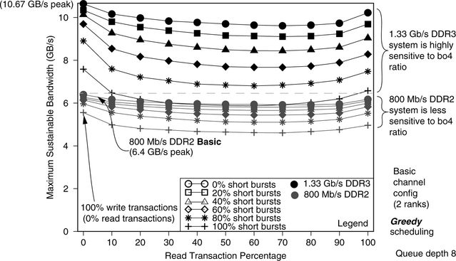
15.4.9 Burst Chop in DDR3 SDRAM Devices
One consequence of the 8-bit prefetch length of the DDR3 device is that the natural burst length in DDR3 SDRAM memory systems is 8 beats. In the case where only 4 beats of data are needed, DDR3 devices implement a burst chop mechanism where an 8-beat burst can be chopped so that only 4 beats of data are transmitted to or from the DRAM device. However, the burst chop mechanism does not allow the DRAM device to pipeline data from the same bank or another bank on the same device after a burst is chopped. The reason that the burst chop mechanism does not allow 4 beat bursts to be pipelined is that the I/O gating structure on the DDR3 device is designed to transport 8 consecutive beats in a single data burst, and the data bus simply idles after a read burst is chopped. Figure 15.27 illustrates that in a DDR3 memory system, a DDR3 device cannot be pipelined consecutively from different banks for the 4-beat (short) burst. Consequently, the only real benefit to the burst chop mechanism is that it allows better data bus utilization in dual rank memory systems, where the rank switching overhead may be shorter than the (same rank) burst chop idle time.

Currently, the DDR3 device architecture as defined by JEDEC does not allow seamless burst merging on the data bus between 4-beat-long bursts from different banks. Rather, the I/O interface of the DDR3 device remains idle for the second half of the 8-beat burst when the standard burst chop mechanism is used to reduce the burst length of the access request. The study in this section examines the gain in sustainable bandwidth when the I/O interface of the DDR3 device is modified to allow the quasi-4-bit prefetch bursts to and from different banks within the same rank of DDR3 SDRAM devices to be seamlessly merged. In this section, three different short burst merging mechanisms are described and compared: the standard (STD) burst chop burst merging mechanism, the short write burst bank switching (WBS) burst merging mechanism, and the short read burst and short write burst bank switching (RWBS) burst merging mechanism. These mechanisms and their respective impact on the DDR3 SDRAM-access protocol are described in the following sections.
Standard (STD) Burst Chop
The standard (STD) burst chop mechanism is the standard mechanism that exists in the DDR3 SDRAM protocol. The STD burst chop mechanism simply terminates the transmission of the second half of the 8-beat burst in the case where a burst chop and the DRAM device I/O interface cannot handle another data burst until two clock cycles later. Figure 15.28 shows the timing of six short column access commands—three short column read access commands and three short column write access commands—for a DDR3 memory system that implements the STD burst chop mechanism. Figure 15.28 shows that in the STD burst chop mechanism, a read burst chop forces the data bus to remain idle for two clock cycles in between two short column read commands to different banks of the same rank, while the timing of two short column read commands to different ranks depends on the rank-to-rank switching time, assumed to be one clock cycle in Figure 15.28. The figure also shows the timing of the short write bursts in the STD burst chop mechanism, and the data bus idles for two clock cycles between two short column write access commands to different banks of the same rank. In contrast, the DRAM controller can direct two short column write access commands to different ranks without having to insert idle cycles between the short bursts on the data bus. That is, Figure 15.28 assumes a data bus termination scheme that allows the memory controller to direct consecutive, bo4 write requests to different ranks without incurring a bubble in the command scheduling timing. In general, the study of the STD burst chop mechanism follows the protocol table as defined in Table 15.8. The timing parameter values for all studies are as defined in Table 15.7.

Short Write Burst Bank Switching (WBS)
The short write burst bank switching (WBS) burst merging mechanism is a mechanism designed to improve the short burst bandwidth characteristics of DDR3 devices. The proposal is based on the premise that it would be simple for the I/O interface of the DDR3 device to be redesigned to support consecutive short write bursts to different banks within the same rank of DDR3 SDRAM devices, but more difficult to merge consecutive short read bursts from different banks within the same rank. Figure 15.29 shows the timing on the data bus of a DDR3 SDRAM memory system that implements the WBS burst chop merging mechanism for the same six short column access commands as illustrated in Figure 15.28. Figure 15.29 shows that in the WBS mechanism, the timing between consecutive, short column read commands is not changed from the STD burst chop mechanism. However, Figure 15.29 shows that with the ability to write short bursts to different banks consecutively, WBS allows DDR3 SDRAM devices to seamlessly merge short write bursts to different banks of a given rank, as well as to different ranks of DRAM devices.
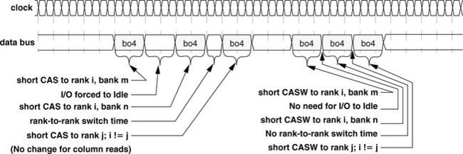
Table 15.9 shows the minimum timing constraints for column write commands to column write commands in a DDR3 SDRAM memory system that implements the WBS short burst merging mechanism. Table 15.9 shows that the only change that the WBS short burst merging mechanism makes to the protocol table is in the case of consecutive column write commands to different banks of a given rank. Unlike the case where consecutive column write commands are made to the same bank, the timing of two consecutive column write commands to different banks of the same rank in Table 15.9 depends on the length of the request itself.

Switching (RWBS)
The short read burst and write burst bank switching (RWBS) burst merging mechanism is the more aggressive mechanism proposed to improve the bo4 bandwidth characteristics of DDR3 devices. The RWBS proposal requires the I/O interface of the DDR3 device to be redesigned to support consecutive, short read bursts and short write bursts to and from different banks within the same rank of DDR3 SDRAM devices. Figure 15.30 shows the timing on the data bus of a DDR3 SDRAM memory system with devices that implement the RWBS burst chop merging mechanism for the same six short column access commands as illustrated in Figures 15.28 and 15.29. Figure 15.30 shows that with the redesign of the I/O interface to implement the RWBS mechanism, consecutive, short read data bursts from different banks of the same rank can be pipelined consecutively without any idle time on the data bus.

Table 15.10 shows column read-to-read and write-to-write timing constraints for the DDR3 SDRAM protocol that accounts for the RWBS short burst merging mechanism. Table 15.10 shows that the RWBS short burst merging mechanism changes the minimum timing constraints for consecutive column read commands and consecutive column write commands to different banks of the same rank. In both cases, implementation of the RWBS short burst merging mechanism means that the minimum timing between consecutive column accesses to different banks of the same rank depends on the requested burst transfer length rather than the 8-bit prefetch length of the DDR3 SDRAM device.

Simulation Results
The simulations in this section assume the basic channel configuration with a single 64-bit-wide channel and 2 ranks of DDR3 SDRAM devices in the single channel memory system. The timing parameter values of the DRAM memory system are as described in Table 15.7. For each simulation, the percentage of read transactions in the input stream is set at a specific value, and the percentage of transactions with a request bo4 rather than bo8 is also set at a specific value. In this work, the percentage of read transactions and the percentage of short bursts are the two independent variables used to characterize the performance benefit of the two different short burst merging mechanisms.
Figure 15.31 shows the maximum sustainable bandwidth of a single channel, dual rank, closed-page, no refresh, 1.33 Gbps DDR3 memory system with a memory controller that uses Greedy command scheduling to achieve maximum sustainable bandwidth.
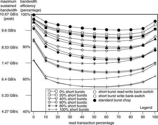
Figure 15.31 shows the bandwidth characteristics of the DRAM memory system subjected to different percentages of read transactions and different percentages of short bursts. In Figure 15.31, the x-axis shows the different read percentages, and different curves show the bandwidth characteristics of the memory system for a given percentage of short burst requests in the input stream. Comparatively, the y-axis of Figure 15.31 shows the bandwidth efficiency and the maximum sustained bandwidth of the memory system. Figure 15.31 shows that the memory system achieves the highest bandwidth with 100% write requests with 0% short bursts. Figure 15.31 also shows that the WBS burst merging scheme gains minimal bandwidth, and the RWBS burst merging mechanism achieves significant gains in bandwidth with higher read request and higher short burst request percentages.
Finally, Figure 15.32 shows the improvement in bandwidth of the RWBS burst chop merging mechanism over the STD burst chop merging mechanism in a 3D graph. Figure 15.32 presents the same data as Figure 15.31, but focuses specifically on the bandwidth improvement of the RWBS burst chop merging mechanism over the STD burst chop merging mechanism, with better grid resolutions for the short burst percentage. Figure 15.32 confirms the intuitive notion that the benefits of the RWBS burst chop merging mechanism over the STD burst chop merging mechanism increases with higher percentages of read requests and higher percentages of short requests.

15.4.10 Revisiting the 8-Bank and 16-Bank Issue with DRAMSim
In DDR3 SDRAM devices, the 8-bit prefetch architecture enables DRAM design engineers to significantly increase the data rate of DRAM device interface while maintaining a relatively low activity rate for the DRAM cell arrays. However, the high interface data rate and relatively constant row cycle times require higher degrees of bank parallelism to maintain a given level of bandwidth efficiency. In this section, the bandwidth characteristics of the 8-bank DDR3 device are compared to the bandwidth characteristics of a hypothetical 16-bank DDR3 device. The basis of the comparison is a 64-bit-wide, 1.33 Gbps DDR3 SDRAM memory system configured in the Basic channel configuration. The Greedy scheduling algorithm is used throughout, and the input stream consists of 0% bo4 requests and 50% read transactions.
Figure 15.33 compares the sustainable bandwidth characteristics of four different system configurations: a 1 rank, 8 banks per rank (1R8B) system; a 1 rank, 16 banks per rank (1R16) system; a 1 rank, 8 banks per rank (2R8B) system; and a 2 rank, 16 banks per rank (2R16) system. In the 8-bank versus 16-bank comparison, all timing parameters are held as constants across all configurations. The difference in each respective configuration is limited to the number of ranks and the number of banks. Figure 15.33 shows that while the 1R16B system configuration achieves significantly higher bandwidth than the 1R8B configuration, the 2R8B system also outperforms the 1R16B memory system by nearly the same margin of sustainable bandwidth; the exact differential in sustainable bandwidth depends on the value of the rank-to-rank switching penalty. Finally, Figure 15.33 also shows that the 2R16B memory system can provide substantial benefit in sustainable bandwidth over the 2R8B memory system, although the benefit of having more banks decreases with increasing queue depth.
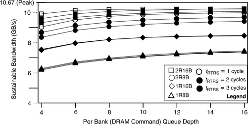
Figure 15.34 shows the same data as Figure 15.33, but cross compares the various system configurations in terms of percentage improvements of sustainable bandwidth. In each case, the system configuration with the lower sustainable bandwidth characteristic is used as the baseline, and the graph illustrates the percentage of bandwidth improvement of having a 16-bank, 1.33 Gbps DDR3 SDRAM device over that of an 8-bank, 1.33 Gbps DDR3 device in different system configurations with different queue depths and rank-to-rank switching penalties. Figure 15.34 shows that upwards of 40% improvement in sustainable bandwidth can be obtained by the 2R8B configuration over the 1R8B configuration. Figure 15.34 also shows that the 1R16B configuration improves sustainable bandwidth over that of the 1R8B configuration between 15 and 21%. Finally, Figure 15.34 shows that the 2R16B configuration improves sustainable bandwidth over that of the 2R8B configuration between 4 and 12%.
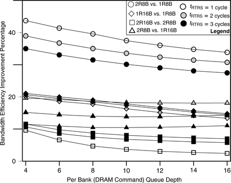
The immediate conclusion that can be drawn from Figure 15.34 is that dual rank memory systems have the greatest benefit in terms of increased bandwidth over single rank memory systems, and the contributing bandwidth benefit of the 16-bank DDR3 device over that of the 8-bank DDR3 device is roughly half of the bandwidth benefit of dual rank memory systems over single rank memory systems. Also, the respective bandwidth benefits of dual rank and 16-bank memory systems over single rank and 8-bank memory systems generally decrease with increasing queue depths.
15.4.11 8 Bank vs. 16 Banks — Relaxed tFAW and tWTR
Figures 15.33 and 15.34 show that a substantial increase in sustainable bandwidth can be obtained with a 16-bank DRAM device over that of an 8-bank device. However, the dual constraints of tFAW and tWTR greatly limit the maximum sustainable bandwidth of single rank memory systems. In this section, we explore the effects of tFAW and tWTR on the sustainable bandwidth characteristics of different memory system configurations.
In Figures 15.33 and 15.34, the simulations are performed with the assumed timing parameters from Table 15.7, and the parameter values listed in Table 15.7 for tFAW and tWTR are 20 cycles and 5 cycles, respectively. To relax the constraints imposed on the DRAM memory system, we repeat the simulations used to obtain Figures 15.33 and 15.34, but with redefined tFAW and tWTR parameter values of 16 cycles and 3 cycles, respectively. All other parameter values remain unchanged from those listed in Table 15.7.
Figure 15.35 shows the maximum sustainable bandwidth of a single channel, 1.33 Gbps DDR3 SDRAM memory system with both sets of tFAW and tWTR parameter values. Figure 15.35 shows that with the relaxed tFAW and tWTR parameter values, the largest gain in sustainable bandwidth over that of the more restrictive tFAW and tWTR values can be found in the 1R16B system configuration, and a smaller gain in sustainable bandwidth can be found in the 1R8B system configuration. In contrast, relaxing tFAW and tWTR impacts the dual rank system configurations to a far lesser degree.

Figure 15.36 shows the cross comparison of the various system configurations with the relaxed tFAW and tWTR values. Figure 15.36 shows that with the elimination of tFAW in combination with the reduced write-to-read turnaround time, the increase in sustainable bandwidth in a 1R16B system over that of a 1R8B system is now a relatively constant 25%. Figure 15.36 also shows that with the elimination of tFAW in combination with the reduced tWTR, the differential in sustainable bandwidth between 1R16B and 2R8B systems drops to single digit percentages. In the extreme case of tRTRS equal to 3 cycles and a queue depth of 16, the 1R16B configuration can, in fact, sustain higher bandwidth throughput than the 2R8B configuration.

15.4.12 Effect of Transaction Ordering on Latency Distribution
In modern uniprocessor and multi-processor systems, multiple memory transactions may be sent to the memory system concurrently. In case the memory system is not immediately available to service a memory transaction, or if a memory transaction is deferred to allow a later transaction to proceed ahead of it, the latency of the later transaction will decrease at the expense of the increased latency of the prior memory transaction. However, if the transaction or DRAM command reordering algorithm results in a more efficient utilization of the memory system, then the average memory-access latency for all memory transactions will decrease. Figure 15.37 shows the impact of a Command Pair Rank Hopping (CPRH) scheduling algorithm on the memory-access latency distribution for the 179.art through 2 billion instructions as compared to the First Come First Served (FCFS) scheduling algorithm.3 The memoryaccess latency distribution illustrated in Figure 15.37 is obtained by a mechanism that records the access latency for each memory transaction in the bus interface unit (BIU) between the processor simulator and DRAMSim. In the simulation framework, each time a memory transaction is sent to the BIU, the start time of the transaction is recorded by the BIU. Upon completion of the memory transaction, the BIU simply computes the latency and keeps track of the number of transactions for each specific latency value.
In the simulated memory system, the minimum latency of a memory transaction is simply the delay through the BIU added to the delay of the memory controller and the minimum DRAM latencies of tRCD + tCAS. In the simulated memory system, the delays through the BIU and memory controller are set to 10 ns, and the minimum access latency is approximately 30 ns for the set of timing values used in this study and illustrated in Figure 15.37. Figure 15.37 shows that the CPRH scheduling algorithm greatly decreases the queueing delay for many pending memory transactions in 179.art, and the number of transactions with memory-access latency greater than 400 ns is significantly less than the same workload operating with the FCFS scheduling algorithm.
In Figure 15.37, the memory-access latency distribution curve graphically illustrates the benefits of the CPRH algorithm for 179.art. However, just as the memory-access latency distribution curve can be used to illustrate the benefit of the CPRH scheduling algorithm, it can also be used to illustrate possible problems with the CPRH scheduling algorithm for other workloads. Figure 15.38 shows the latency distribution curve for 188.ammp, and 188.ammp was one workload that points to possible issues with the CPRH algorithm. Figure 15.38 shows that the CPRH scheduling algorithm resulted in longer latencies for a number of transactions, and the number of transactions with memory-access latency greater than 400 ns actually increased. Figure 15.38 also shows that the increase of a small number of transactions with memory-access latency greater than 400 ns is offset by the reduction of the number of transactions with memory transaction latency around 200 ns and the increase of the number of transactions with memory-access latency less than 100 ns. In other words, the CPRH scheduling algorithm redistributed the memory-access latency curve so that most memory transactions received a modest reduction in access latency, but a few memory transactions suffered a substantial increase in access latency. The net result is that the changes in access latency cancelled each other out, resulting in limited speedup for the CPRH algorithm over the FCFS algorithm for 188.ammp.

15.5 A Latency-Oriented Study
In the previous section, we examined the impact of transaction ordering on the memory-access latency distribution for various applications. Memory controller schedulers typically attempt to maximize performance by taking advantage of memory application access patterns to hide DRAM-access penalties. In this section, we provide insight into the impact that DRAM architectural choices make on the average read latency or memory-access latency. We briefly examine how the choice of DRAM protocol impacts memory system performance and then discuss in detail how aspects of the memory system protocol and configuration contribute to the observed access latency.4
15.5.1 Experimental Framework
This study uses DRAMSim, a stand-alone memory subsystem simulator. DRAMSim provides a detailed execution-driven model of a Fully Buffered (FB) DIMM memory system. The simulator also supports the variation of memory system parameters of interest, including scheduling policies and memory configuration, i.e., number of ranks and channels, address mapping policy, etc.
The architecture modelled is shown in Figure 15.39. The memory controller comprises read and write transaction queues for each channel, from which commands and command frames are scheduled to the channel. The memory trace inputs are all placed in the BIU. The BIU is set to be infinite in size for the limit studies. For the trace-driven studies, we use a BIU which can hold as many outstanding transactions as the combined transaction queue capacity. The read and write transaction queues, which are equal in size, can hold 32 transactions—16 active reads and writes. Transactions are moved to a response queue (not shown in the figure) after they are scheduled to the memory modules. Read transactions remain in the response queue till the read data returns, while write transactions are retained till completion.
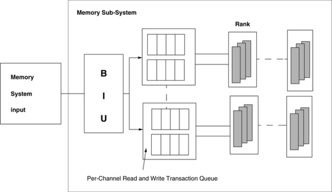
FIGURE 15.39 Memory controller architecture. The figure shows the basic architecture of the memory controller modelled in DRAMsim and used for these experiments. The figure also shows the memory system inputs used to drive the simulator. Memory requests are issued into the BIU either froma file created by a random address generator or from a memory request trace file obtained from microprocessor simulation infrastructures. Note that for the limit studies using a random address generator, we assume that the BIU is infinite in size. For the microprocessor trace-based studies, we use a fixed-size BIU.
The memory controller scheduler builds a schedule using an algorithm that prioritizes read transactions over write transactions. Natarajan et al. [2004] and Ganesh et al. [2007] have demonstrated in their papers that a memory controller that prioritizes read over write transactions achieves significant performance improvement over one that does not. This scheduling rule is maintained except when the read and write transactions are to the same location in memory. In general, older transactions of a given type are given priority over transactions of the same type that arrived later. An older read transaction can be scheduled later than a newer read transaction if the required resources are available later.
We studied two different DRAM types: a conventional DDR2 system with a data-rate of 667 Mbps, and its corresponding FB DIMM systems: an FB DIMM organization with DDR2 on the DIMM. FB DIMMSare modelled using the parameters available for a 4-GB module [Micron 2005]; DDR2 devices are modelled as 1-Gb it parts with 8 banks of memory [Micron 2006]. The microprocessor driver is assumed to be running at 4 GHz. In this particular study, we focus on closed-page systems which are commonly used in the server space. It is common in such a case to use posted CAS, i.e., the RAS and CAS are transmitted to the memory controller in the same cycle. For FB DIMM systems using posted CAS, the RAS and CAS are placed in the same frame. We also assume that each DIMM has only a single rank of memory.
15.5.2 Simulation Input
There are two types of inputs used to drive the simulations:
Random Address Traces
These input traces are generated using a random number generator. The input address stream is modelled as a poisson arrival process where each request is independent of the previous request. Each random address stream is identified using the following parameters:
• Average issue bandwidth is the average arrival rate for the Poisson process used to model the trace.
Since the commonly observed ratio read to write traffic is 2:1, the input traces are set to have a 2:1 ratio of read to write traffic. The traffic is distributed equally to all the ranks in the system.
Application Traces
Input traces from the SPEC workloads in combination to generate 2, 4, and 8 way multi-programming traces. The application traces used in this study were generated using simalpha [Desikan et al. 2001] using a processor configuration with a 1MB 8-way set associative L2 cache with a 64-byte cacheline. All traces were collected after fast-forwarding the application by 2 billion instructions and executing for 200 million instructions. The applications are grouped together to form workload mixes which are memory intensive. Note that the classification is based on the behavior of the workload in the region when the traces are grabbed.
15.5.3 Limit Study : Latency Bandwidth Characteristics
One of the commonly used approaches to gauge the performance of a memory system protocol is to conduct a limit study using random-address traces as input. The latency and bandwidth values are measured for a random address trace whose input arrival rate is varied. The latency typically gradually increases till a particular bandwidth value after which it dramatically increases. This point on the latency-bandwidth curve represents the maximum sustainable bandwidth of the system prior to its getting overloaded. Memory controller design is focussed on moving this latency-bandwidth curve to the right, i.e., improving the read latency values at higher bandwidth values. Figure 15.40 shows the latency bandwidth characteristic of a DDR2 and FB-DIMM DDR2 system. The graphs are shown for the FB-DIMM DDR2 system in fixed latency mode.

FIGURE 15.40 DDR2 and FB-DIMM-DDR2 latency bandwidth characteristics. The figure shows the latency bandwidth characteristics of a DDR2 and FB-DIMM DDR2 system. The graphs are generated using a random-input address trace with 66% read traffic and varying input arrival rate. A transaction is equally likely to be addressed at any of the given banks in the system.
We observe that the maximum sustainable bandwidth of a multi-rank FB-DIMM system is approximately 25% times greater than that achieved by a multi-rank DDR2 system. The increased sustainable bandwidth is due to the increased DIMM-level parallelism in an FB-DIMM system and the additional available data-bandwidth. The separation of the read and write data buses from the memory controller to the DIMMs enables the memory controller to keep simultaneously scheduled read and write transactions to two ranks on two different DIMMs. This factor contributes to being significantly higher than that seen in a DDRx system.
The single rank configuration has the lowest maximum sustainable bandwidth for both systems. In a single rank channel, the DIMM emerges as a significant bottleneck due to the constraints imposed by the various DRAM timing parameters. Increasing the number of ranks from 1 to 2 significantly improves the maximum sustainable bandwidth by reducing the contention for the DRAM banks. Further increases in the number of ranks in the channel have no impact in DDRx systems because of the increasing competition for the bus. In the case of FB-DIMM systems, doubling the number of ranks from 2 to 4 has marginal impact while going from 4 to 8 ranks has almost no impact. We observed that typically the reduction in the queueing delay due to the DRAM availability is replaced with that of the channel being unavailable.
15.5.4 Latency
In this section, we look at the trends in latency, and the factors impacting them, in further detail. Figure 15.41 shows the average read latency divided into queueing delay overhead and the transaction processing overhead. The queueing delay component refers to the duration the transaction waiting in the queue for one or more resources to become available. The causes for queueing delay include memory controller request queue availability, south link availability, DIMM availability (including on-DIMM command and data buses and bank conflicts), and north link availability. Note that the overlap of queueing delay is monitored for all components except the memory controller request queue factor. The default latency cost is the cost associated with making a read request in an unloaded channel.

FIGURE 15.41 Read latency for various configurations systems with identical numbers of DIMMS are grouped together. Within a group, the bars on the left represent topologies with fewer numbers of channels. The DRAM configuration was FBD-DDR2 using fixed latency mode. The y-axis shows latency in nano-seconds.
The queueing delay experienced by a read transaction is rarely due to any single factor, but usually due to a combination of factors. Changing the system configuration, by adding more ranks in the channel or increasing the number of channels in the system, results in a change in the availability of all the resources to a different degree. Thus, we see that the latency trends due to changes in a configuration are affected by how exactly these individual queueing delays change.
Single-rank configurations experience higher latencies due to an insufficient number of memory banks to distribute requests to and the inability to schedule take advantage of any parallelism the FB-DIMM channel offers. In such systems the DIMM is a dominant system bottleneck and can contribute as much as 50% of the overall transaction queueing delay. Adding more ranks in these systems helps reduce the DIMM-based queueing delays. The reductions are 20–60%, when going from a one rank to a two-rank channel. For 4–8 rank channel, the DIMM-based queueing delay is typically only 10% of that in the single-rank channel.
The sharing of the southbound bus by command and write data results in a significant queueing delay associated with southbound channel unavailability. Since all three memory workload mixes have nearly 33% write traffic we find that the southbound channel is a significant bottleneck. The southbound channel queueing delay is reduced by increasing the number of channels in the system. Some reductions in southbound channel unavailability are also achieved by adding more ranks in the system. In a multi-rank channel, the memory controller is more likely to be able to pack multiple commands in the same frame. Though the opportunities to do so are limited, this can result in a decrease in southbound channel unavailability by 10–20% when increasing the number of ranks in a channel from 1 to 2.
Increasing the channel depth raises the transmission costs for frames on the channel. This results in an increase in the read latency with increasing channel depth for MEM-2 (Figure 15.41(a)) and for the other workloads for larger number of channels, when the utilization is low. Interestingly, the additional DRAM-level parallelism available in a deeper channel can counter the rise in frame transmission costs sufficiently to reduce overall latency (Figure 15.41(b) and (c)). The gains in parallelism are especially apparent when going from a single-rank to a two-rank channel. These gains gradually taper off with further increases in channel depth.
With deeper channels, the increased number of in-flight transactions results in an increase in the queueing delay due to the link-unavailability. This is attributable to the heightened competition for the bus due to the additional number of in-flight transactions. This increase can combine with the increase in processing cost to offset the gains due to increased DIMM-level parallelism. Thus, we see that for MEM-4 and MEM-8, Figures 15.41(b) and 15.41(c) respectively, that the latency increases in a single channel system when the channel depth is increased from 4 to 8.
The interaction of the increase in processing overhead, the number of in-flight transactions using the channel, the type of these transactions and the lowering of DIMM-level conflicts result in the different latency trends observed. Depending on which trend dominates, the latency can increase linearly with the number of ranks in the channel (Figure 15.41 (a)) or decrease initially and then increase as more ranks are added to the channel (Figures 15.41(b) and (c)). In general, the former occurs in a relatively lightly loaded system while the latter occurs in a system with higher bandwidth demand.
Figure 15.42 shows the variation in read latency contributors in a DDR2 system for the MEM-2 and MEM-4 workloads. The latency in a DDRx system unlike an FB-DIMM system changes marginally with the number of ranks in the channel. This is because unlike in an FB-DIMM system, the default latency of an operation does not vary with the number of ranks in the channel for a DDRx system as seen from Figures 15.41 and 15.42. Further, the queueing delay due to DRAM unavailability is replaced by that due to the link being unavailable as the number of ranks in the channel is increased.
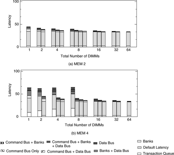
FIGURE 15.42 Read latency for various configurations for DDR2 systems with identical numbers of DIMMS are grouped together. Within a group, the bars on the left represent topologies with fewer numbers of channels. The DRAM configuration was DDR2 using fixed latency mode. The y-axis shows latency in nano-seconds. The y-axis scales are different for graphs.
A single channel configuration for MEM-4 experiences fairly significant queueing delay due to the transaction queues being full. Although the BIU has as many entries as the transaction queue, these entries can hold a read or a write transaction. The distinction between the read and write transaction queues in the memory controller queues results in a write transaction waiting for the transaction queue to become available when the write transaction queue fill up. This in turn delays later read transactions. By enforcing starvation awareness this problem is alleviated marginally but not completely in a busy system.
15.6 Concluding Remarks
The difficulty of sustaining high bandwidth utilization has increased in each successive generation of commodity DRAM memory systems due to the combination of relatively constant row cycle times and increasing data rates—increasing data rates that translate directly to shorter data transport times per bit. The growing disparity between the relatively constant row cycle times and shorter data transport times means that longer requests or larger numbers of requests must be kept in flight by the DRAM memory controller to sustain high bandwidth utilization. For DDR3 SDRAM memory systems, the task of sustaining high bandwidth utilization is made even more complex by timing constraints such as tFAW and tRRD, timing constraints designed to limit the rate of row activation commands in DDR3 SDRAM devices and provide a relatively constant power envelope with increasing DRAM device data rates.
The complexity of the various inter-related constraints in DRAM memory system performance characteristics means that sustaining high bandwidth utilization in a high speed DRAM memory system is a multi-dimensional optimization problem, where sustainable bandwidth depends on factors such as DRAM memory system configuration, DRAM timing parameter values, workload-specific request access sequences, and memory controller sophistication. Fortunately, the increasing sophistication will serve to keep memory system architects gainfully employed for a long time to come.
1The cacheline size is 64 bytes.
2At least 8 queues are needed in the controller for a 1 rank, 8 bank memory system, and 32 queues are needed in the controller for a 2 rank, 16 banks per rank memory system.
3The Command Pair Rank Hopping (CPRH) scheduling algorithm is a patent-pending scheduling algorithm, and the algorithm is not specifically described herein. The simulation results are provided for illustrative purposes only.
4Some of this section’s material appears in “Fully-Buffered DIMM memory architectures: Understanding mechanisms, overheads and scaling,” by B. Ganesh, A. Jaleel, D. Wang, and B. Jacob. In Proc. 13th International Symposium on High Performance Computer Architecture (HPCA 2007). Phoenix, AZ, February 2007. Copyright IEEE. Used with permission.